

Acoustic Screening to Remove Suspect Plastic Components
Testing parts for gaps reveals which parts are electrically intact but prone to future delamination.
In an ideal world, plastic-encapsulated microcircuits (PEMs) would leave the component manufacturer in pristine condition. BGAs, QFNs, PQFPs, TOs and other package types would have no electrical or structural anomalies that could lead to electrical failures. The components would arrive for assembly in this condition, and would pass through handling, reflow and testing with no alteration of their ideal state. They would give years of flawless service.
In the real world, things do not always work out like this. A component may pick up a gap-type structural anomaly – delaminations, voids and cracks are the common ones – somewhere between the molding process and post-assembly shipment. Many of these gap-type anomalies make no difference in the proper functioning or lifespan of the component. Some, though, depending on size and location within the package, can expand until they break a connection. Even without expanding, gaps are the locations where moisture tends to collect, whether it has percolated through the mold compound or entered by a crack along a lead finger. The combination of moisture and contaminants, which can arrive by the same routes, can promote corrosion that may lead to electrical failure.
The least dangerous gap-type PEM anomaly is probably a small void (air bubble) in the mold compound not near to or in contact with any other surface such as a wire or the die. Generally such an anomaly is not considered a defect. Far more dangerous are defects such as delamination between the mold compound and die face. Normal thermal cycling, with repeated coefficient of thermal expansion stresses, can cause the delamination to expand across the face of the die until it shears off a wire bond.
There are numerous other gap-type anomalies, and many pose a greater or lesser threat to electrical performance. The important questions during assembly are:
- What percentage of the components in a given lot has internal structural anomalies?
- How likely are these anomalies to cause eventual electrical failure?
Sonoscan’s applications laboratory, which images lots of components for assemblers, routinely uncovers the answers to both questions. The assembler that will use the components writes the rules that will distinguish harmless anomalies from dangerous defects. Acoustic micro imaging systems image and analyze internal gap-type features, which reflect ultrasound at higher amplitude than other internal features such as the die or lead fingers.
PEMs in which a gap-type feature has already broken a connection will, of course, fail electrical tests. The purpose of acoustic screening is to identify and remove those PEMs that are electrically intact, but that have gap-type defects likely to cause field failures. For commercial products, defects of a certain size may be acceptable if the risk of failure is low. In military, aerospace and medical products, the degree of risk permitted ranges from very low to zero.
The outcome of acoustic screening varies greatly from one lot of components to another. It is not uncommon for a lot of components to have up to 5% rejects. The accept/reject criteria are defined by the user of the part and are applied to internal anomalies visible in the acoustic images.
Acoustic images reveal all sorts of anomalous situations. The ultrasound pulsed into a component is reflected from material interfaces at many depths, but the echoes can be selected by their arrival time to limit the acoustic image to a desired depth. The acoustic image of the BGA in Figure 1 captured the depth from just below the top surface of the mold compound to just above the die, and included the tops of the wires (at center). The red and yellow features are voids in the mold compound. Such isolated voids are generally considered harmless. But this BGA has a great many voids, running down to sizes so small that they get lost in the tiny white features created by the distribution of particles in the mold compound.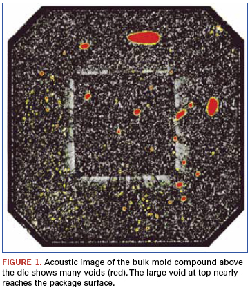
But by using a new technique to image the bulk of the mold compound in many sequential slices, the Sonoscan lab found the real danger: The largest void, at top, extends vertically from the substrate upward almost to the top surface. Moisture and contaminants that percolate through its thin wall have a free ride to the center of the package.
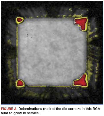
Figure 2 is the acoustic image of the die surface in a BGA that would almost certainly pass electrical tests, but that is loaded with potential disaster. The red areas at each corner of the die face are small delaminations of the mold compound from the die. At this early stage, the delaminations are unlikely to have yet broken a wire bond on the die. The normal thermal cycling of service, however, is what makes die face delaminations so perilous; they may expand laterally until they find and break a wire bond.
A PEM that is being tested in a laboratory that determines Moisture Sensitivity Level (MSL) is initially dried to remove existing moisture, then moisturized to a specific level. It next goes through reflow three times, although it is not soldered to the board, since it will later be sectioned physically. The three passes through reflow simulate the experience of a component on a board that is reflowed twice and is then reworked. After the third reflow, the PEM undergoes a basic electrical test to find opens. It is then screened acoustically to look for gap-type defects, and then physically sectioned to see the defects optically. The acoustic image is the guide for selecting the best location for physical sectioning. Some defects, though dangerous, cannot be seen after physical sectioning because they are too thin. Delaminations as thin as 1 µm reflect virtually all of the ultrasound and are imaged strongly, but such a thin gap may be invisible optically.
MSL test personnel often encounter a PEM whose acoustic image shows multiple problems – voids, delaminations, even cracks – but which passed the electrical tests. Such a PEM may be loaded with structural anomalies that will cause electrical failure under the stress of service, but none of those anomalies happens to have caused a problem yet. In a production environment, such a “train wreck” can sail through basic electrical testing and go right into production.
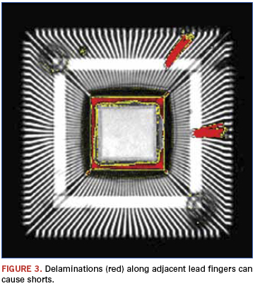
Figure 3 is an acoustic image of a high-risk PEM. It has two types of defects. First, the die paddle is delaminated (red) from the mold compound around the periphery of the die. This is a moderately serious condition; the delamination could expand and move under the die and the die attach material. But in two locations on the lead fingers is another dangerous condition: delaminations on adjacent lead fingers. The wall of mold compound between the lead fingers is very thin, and can easily be dissolved by corrosion, causing a short between the lead fingers.
The same result – a short between adjacent lead fingers – can be triggered by a different mechanism often encountered in Sonoscan’s laboratories. In some PEMs, the tape (white in Figure 2) looks red or yellow in the acoustic image because it is delaminated from the mold compound. Although frequently considered unimportant, corrosion along such a delamination can also put two adjacent lead fingers in electrical contact.
The locations and types of gap-type defects are largely determined by the package design. Delamination of the mold compound from a lead finger, for example, may not even be considered a defect if a package has long lead fingers on which there are a few small delaminations. They are unlikely ever to grow sufficiently to like the outside atmosphere and the die or the wire bonds. But a package design having a very small die and very long wires connected to very short lead fingers is a different story. The distance from the outside atmosphere to the outer wire bonds is very short, and can be bridged even by a small delamination. The very long wires are also vulnerable to wire sweep during molding.
One of the defects MSL test personnel expect to see in some PEMs is the popcorn crack. Popcorn cracks form when moisture within the package turns to steam during reflow and expands in volume by about 1600 times. Popcorn cracks are not as frequent in production as they were a decade or two ago, but they still occur. They usually originate at the die attach level and travel downward to the bottom surface of the package. Very few travel to the top surface, and even fewer go sideways. A popcorn crack exiting the bottom of the package is invisible during production, but over the life of the components provides a convenient path for moisture and contaminants to reach the die.
Acoustic screening uncovers all sorts of things. Die face delaminations have a reputation for being lethal, but there are a very few specific packages in which, users
have found, small die face delaminations practically never cause electrical failure, probably because of a lucky combination of design and materials. Acoustic screening lets the user check the initial state of these delaminations. Another user might find that a lot of familiar PEMs suddenly shows numerous, large delaminations in a large percentage of components. These may be counterfeit PEMs, starting on their second lifetime of service. Or the defects may simply result from a change in mold compound or fabrication processes.
The most dramatic outcome of acoustic screening is the avoidance of mass field failures. In less dramatic scenarios, the weeding out of problem components gives a boost to overall product reliability.
Tom Adams is a consultant at Sonoscan Inc. (sonoscan.com); tom100adams@comcast.net.


Press Releases
- Niche Electronics Celebrates Completion of Florida Expansion
- Microscreen Names Nik Thomas Director, Expands Leadership Role Amid Continued Organizational Growth
- W&S Enters New Growth Phase Through Strategic Partnership and New Leadership
- Federal Electronics Expands Environmental Testing Capabilities with New Extended-Range Thermal Test Chamber