

Board Repair Made Easy
Modifying small form-factor PCBs using preformed pads can save thousands in tooling costs.
Need to fix a PCB? Easy. Need to fix a substrate or interposer? Not easy.
A number of variables contribute to the level of difficulty, but the primary delta is the difference in pad and trace size. Repair kits are available for large form factor boards with their larger feature sizes, but smaller form factor boards (and features) are not as readily available.
For larger pads and traces on traditional PCB designs, suppliers offer repair kits containing various combinations of pads, traces and lands. Larger and wider pads can be fabricated with various techniques to yield copper and copper base metal solutions with and without enhanced solderable surfaces. Tighter aspect geometries (less than 150µm) prove more difficult than larger pitch (400µm and wider) geometries.
Traces are narrow; metallization is thinner, and it is possible that metal finishes might not suit solder profiles; for example, thick gold on small pads can lead to embrittled solder joints with small flip chip bumps. As a result of these smaller geometry requirements on small form-factor boards, fabrication techniques prove more difficult due to undercutting on etch solutions and any number of issues with laser-cutting (heat damage, inability to cut fine geometries, metal curling and subsequent plating issues) and flatness when stamping or punching.
For small or standard form-factor PCBs, “modification,” not repair, can be required. Metal shielding, an extension to a power or ground plane, addition of a passive or active component, or any other modification are design changes that might need to be reviewed prior to investments in new die and boards. Removing failed devices can cause lifted pads, damaged traces, and corrupted metallization that require repair. Repair is a better solution than scrapping or ordering replacement boards. Both can be expensive, of course, and lead to delays, and in some cases do not yield acceptable results, resulting in scrap.
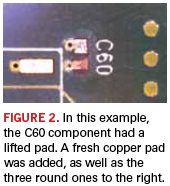
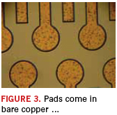
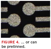
A new novel board repair kit includes fabricated traces and pads, which are then placed on the board (Figure 1). Custom shapes are available, as well as standard circular and round pad sizes of 150, 200, 250, and 300µm geometries (Figure 2). Pad sizes in sub 100µm geometry footprints with and without traces/tails can be fabricated as well. Base metals of copper can be plated with ENIG, gold, SAC, tin, and SnPb (Figures 3 and 4). Sidewalls have less than 5% taper, so tight geometries can be fabricated. (Spiral inductors have been fabricated with spaces less than 6µm on 10µm wide traces.)

In many cases, especially for high-frequency boards, modifying the board is less expensive than repairing it. In some cases, the pads have been mounted on boards and used as antennas.
In one instance, four modifications were performed on a series of buildup boards, saving the customer considerable time and expense. “We are very pleased in the ability to solder down the flip-chip substrates, and it allowed us to test modifications on the substrate at a speed that would be impossible through the normal substrate design cycle of ~1.5 months,” said Francisco Ledesma of nVidia. “The process allowed us to try several substrate modifications without incurring the large expense of redesigning the layout several times. In the end, this provided us fewer design iterations, less time and lower cost.” Given that tooling charges for buildup boards can cost up to $50,000 to $80,000, it is estimated the customer saved more than $200,000 in tooling costs alone.
Turn times are typically less than one week. Structures can be shipped on gel packs, inside vials, tape and reel, or in custom packages.
Terence Q. Collier is president of CVinc (covinc.com); tqcollier@covinc.com.


Press Releases
- XLR8 EMS Welcomes Raul Jorge Lopez Jr. as Director of Program Management and Procurement
- Koh Young America Promotes Ramiro Mora to Lead Service and Applications in Mexico and South America
- ViTrox Americas Welcomes Huy Pham as Technical Support Engineer
- XLR8 EMS Appoints Steve Dutton as Chief Sales Officer