Programming-Free, AI-Powered Visual Quality Inspection (VQI)
New advances permit defect detection in a fraction of the time.
Despite the prevalence of automated optical inspection (AOI) systems for PCBA manufacturing processes, many organizations still rely on manual inspection for the post-SMT stage of production.
However, three overlapping trends – 1) the industry’s well-documented labor shortage that’s poised to worsen; 2) the projected 15% year-over-year growth in PCB manufacturing; 3) the migration of sensitive electronics manufacturing work back to North America – are obliging organizations to examine automated solutions for manual aspects of their workflow.
To this end, the latest advances in artificial intelligence (AI) – the “second wave” of AI characterized by machine learning and deep learning technologies – means that manufacturers can finally reap the rewards of reliable and high-performance automated inspection for the post-SMT and final assembly stages of production.
What AI Means for Assembly
Deep learning is a ubiquitous technology that excels at image identification tasks, and the state-of-the-art has enabled the creation of high-performance models that remain computationally efficient. But, at the risk of sounding flippant, so what?
In the book Prediction Machines,1 three eminent economists recast the rise of AI as a drop in the cost of prediction: that is, of taking a set of inputs and producing a highly accurate output.
In the context of electronics manufacturing, one application of this technology is to ingest a set of high-resolution digital images of a PCB/PCBA and to output a prediction as to whether the board meets specific quality criteria.
As you’ll see, this permits organizations to augment human eyeballs with cameras and artificial intelligence to realize certain productivity gains.
Moving from concept to reality, artificial intelligence enables the creation of automated visual quality inspection (VQI) systems at the back-end/final-assembly portions of the PCBA process that:
- Can identify defects more accurately than human operators
- Can identify defects in a fraction of the time vs. human operators
- Perform consistently and improve over time
- Can be programmed for new products in minutes
- Contribute to Industry 4.0 initiatives such as digitization.
The primary benefits of the system include higher production throughput, reduced demands for personnel, significant reductions in scrap, and an overall decrease in the cost of poor quality (COPQ).
At the same time, the data captured and generated by VQI systems unlocks second-order benefits, such as digitization and predictive analytics that are of interest to many technology executives.
Today’s AI-based systems are versatile enough to handle high-mix PCBs and can be installed practically anywhere in a production line, including the post-SMT stage. Such flexibility permits manufacturers to implement VQIs at multiple inspection points, to improve both overall inspection performance, and to gain comprehensive digital records that extend through the entire PCB production lifecycle.
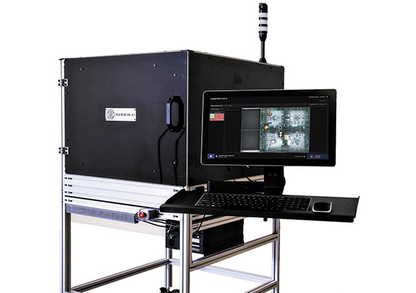
DarwinAI has developed a new complete, purpose-built solution, called the Automated Mixed-Assembly Inspection (AMI) system, in partnership with leading OEMs and electronics manufacturing services (EMS) companies. Within the PCB production environment, the hardware can be deployed as:
- Inline systems (FIGURE 1), typically located either at the end of SMT, or pre- or post-solder
- Standalone systems ideal for high-mix, low-volume environments where boards are being placed manually, or at repair stations where the system performs inspection once repairs are complete
- Benchtop systems, which retain the same performance level as the standalone model, but are designed with mobility in mind and thus have a smaller footprint.

Figure 1. Inline production deployment of a DarwinAI AMI system.
To gather quality images of the board under inspection – the product can handle board sizes up to 24" x 24" – the system’s optics incorporate a 20MP colored camera with a global shutter, a 25mm focal lens and polarizers, and a strobing white ring light. The field of view is 5" x 5", and the system can accommodate boards up to 25" x 25" by taking multiple images. The operator interacts with the AMI system via an integrated 19.5" P-CAP Premio touch monitor.
The system also contains all the computing resources (e.g., actuator and strobing controllers, computational capacity) necessary to control the hardware and power the software, which itself includes a few notable components:
- Component detection system: a deep learning model that examines images of PCBs and automatically isolates individual components
- Defect identification system: a deep learning model that examines images of components and identifies an array of defects
- Explainable AI (XAI) module: understands the visual regions and factors that influenced the defect identification system’s inspection conclusions; essential to providing transparency and building operator trust
- Inspection UI: a straightforward interface used both to configure the AMI system and to conduct inspections.
Addressing the Data Problem with Generative AI
One key obstacle to applying general vision AI systems to PCBA inspection is the dependence on training data, along with the associated overhead and effort needed to collate the large, labeled datasets that machine learning systems require. Manufacturing contexts are especially challenged by this impediment, as images of component defects are scarce.
In our experience, about half of manufacturers have the data, but it’s rarely in a format conducive to building an AI system; whereas the other half lack the hardware imaging capabilities to obtain data of sufficient quality for AI applications. Taken together, these observations suggest that very few manufacturers are equipped to develop an AI-based inspection system in-house or to train a purpose-specific AI system in a timeframe conducive to economic payback.
The AMI system eliminates this problem in two key ways.
First, the system is pre-trained on an extensive dataset of labeled PCB images. In practical terms, the system already knows how to interpret PCB images, recognize individual board components, and identify:
- SMT defects: missing component, wrong component, wrong resistor value, wrong polarity, skewed components, tombstoning, bent IC pins, cracks and chips; and
- Through-hole (THT) defects: missing component, wrong polarity.
Second, is a piece of IP our organization developed regarding a technology that’s becoming increasingly ubiquitous called generative AI.
As the name suggests, generative AI involves the generation of novel and useful artifacts by an artificial intelligence system. ChatGPT, the renowned tool from OpenAI, utilizes the technology in key ways to generate language that human beings find convincing.
How is this technology used for something as different as PCB analysis? Recall that AI requires data in order to learn.
In our industry, it needs examples of component defects that are valuable to identify in a PCBA context (missing components, bad orientations, tombstones). Given that many manufacturing organizations already run efficient processes, such anomalies – what is sometimes termed “negative data” – can be difficult to obtain.
To this end, our research team was able to exploit the principles of generative AI to produce “synthetic data” for PCBs and defects, which was in turn used to train the AMI system to produce quality results. Moreover, whereas a user cannot necessarily trust the output of ChatGPT, an operator can trust the results of our AMI system by asking it to “explain” how it reached a particular conclusion by way of the aforementioned XAI module.
As a result of these technologies, the only information the AMI system requires to begin operation is a reference image of each model (i.e., a golden board). As such, configuring a new board model for inspection takes less than five minutes – a stark departure from many AOI systems.
5-Minute System Configuration
Configuring the AMI system doesn’t require any rules-based or code-based programming. Instead, to create a new board profile, a quality engineer enters the model number and the physical dimensions of the board and places a golden board in the inspection/imaging chamber. From there:2
- The AMI system captures images of the board.
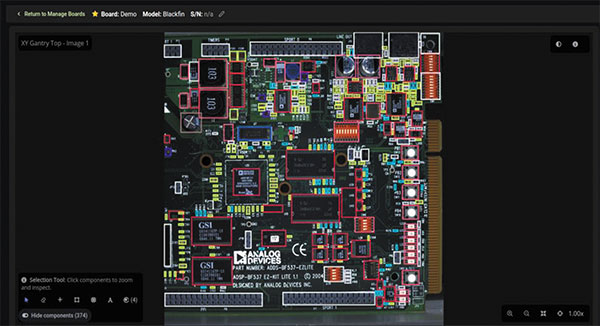
- The system automatically detects all board components, classifies them accordingly, and presents a map to the quality engineer.
- The quality engineer reviews the classification (FIGURE 2), overrides any misclassified components, and approves the board profile.

Figure 2. During the configuration process, the inspection UI shows the board components to the operator, with different components bounded by different colors; quality engineers can customize the interface to show different colors.
At this point, the model’s board profile is complete and the system can be used for production inspections.
Given material and component shortages, a manufacturer will sometimes stipulate that alternative components may be used on a given product (e.g., an alternate resistor).
To this end, an alternate component feature allows for the “union” of multiple golden boards, with the AI detecting automatically if a new component is an acceptable alternative to the reference standard. Such flexibility permits the AMI system to adapt to manufacturing realities including board refinements and component swaps, without incurring downtime or other complications.

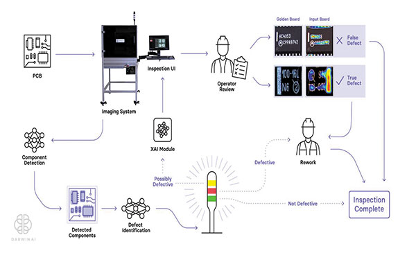
Figure 3. The AMI operates within a human-in-the-loop system that permits faster and more accurate defect identification than either operators or AI-only systems.
The Inspection Process
Inspections are conducted within a human-in-the-loop (HITL) process (FIGURE 3) that begins with an operator selecting the appropriate board profile. From there2:
- The PCB to be inspected is passed into the AMI’s inspection chamber.
- The imaging system captures multiple images of the PCB under inspection.
- The component detection system identifies and extracts images of individual components.
- Component images are passed through the defect identification system, which classifies components as defective, possibly defective, or non-defective.
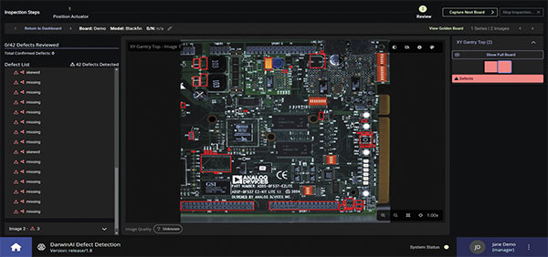
- The inspection UI presents the findings to an operator (FIGURE 4), offering a side-by-side view of the entire board under inspection and the reference golden board; powered by the explainable AI module, the interface visually shows the reason why a particular anomaly was classified as a defect.
- The operator reviews the findings (and is free to zoom in to examine and compare in detail, as needed), validating the AI’s decision or overriding it.

Figure 4. The Inspection UI identifies many component and defect types simultaneously, and clearly presents the findings to the operator, who can approve or override the AI’s conclusions.
By way of this process, the human operator and the AMI system work together to reach levels of performance effectiveness and efficiency that neither could achieve alone. Each inspection outcome further tunes the defect identification system to higher levels of inspection accuracy, creating a feedback loop that enables the overall AMI system to rapidly catch up to the inspection capabilities of a skilled operator, before surpassing – for the entire life of the production line – the limits of human expertise.
Real-World Outcomes
The novel system is in use today at a number of leading OEMs and EMS organizations, each of which has experienced a quick return on investment. This rapid ROI is primarily attributable to significant improvements in several key areas, including (as a composite average):
- 10% more throughput, attributable to less rework time
- 80% less labor required, due to the high degree of automation
- 50% less scrap, as defects are caught earlier.
Perhaps the strongest validation of the AMI system is that most manufacturers that have piloted the solution have either already expanded their deployment or are planning to do so in the near term, based entirely on first-order benefits.
However, the full benefits extend well beyond improvements to the testing process, including second-order benefits that become apparent over a longer timescale. Every inspection produces a complete digital record – including images and metadata – the exportation, aggregation and analysis of which better equips manufacturers to:
- Locate and eliminate the root cause of defects
- Maximize line performance and yield
- Uphold quality standards across the supply chain
- Proactively recognize emerging issues (e.g., component drift as a result of minute changes in placement)
- Perform detailed audits.
Finally, our research team is developing new IP with the intent of tackling some of the “harder” problems in the space. For example, we are still in the early days of exploiting our Second Order Explainability technology that we revealed at MIT last year.3 Process engineers and others interested in learning more about this subject can consult the SolderNet paper we authored in collaboration with the University of Waterloo’s Vision and Image Processing Research Group and Moog Aerospace based in Buffalo, NY.4
Conclusion
Although the benefits of a reliable, automated inspection system are self-evident, deploying new systems in production environments is often a tall order – and manufacturers that have had poor experiences with other technologies may be hesitant to introduce an AI-powered system out of concern that performance will not match the promises.
From our experience working with leading manufacturers around the globe, we recommend an incremental approach that focuses on initial quick wins, perhaps even limited to a single inspection point on a single production line. Executing pilot programs to address known pain points can demonstrate the economic benefits of a new solution while also building familiarity and trust.
Equipped with data demonstrating clear ROI, quality and process engineers can secure wider organizational buy-in as they look to broaden the solution’s applications.
This phased approach also gives an organization time to understand and accommodate any new requirements around data practices before scaling up to automate inspection at multiple points and on multiple lines.
After years of promise – and, yes, a few false starts – AI is transforming production workflows in concrete ways and delivering meaningful ROI. Automated visual quality inspection is proving its ability to not only help PCBA manufacturers mitigate palpable risks in the short term but also its potential to help manufacturers be strongly positioned to leverage transformational technologies in the future. •
References
1. Ajay Agrawal, Joshua Gans and Avi Goldfarb, Prediction Machines: The Simple Economics of Artificial Intelligence, Boston: Harvard Business Review Press, 2018.
2. DarwinAI, AMI demonstration, https://www.youtube.com/watch?v=ge625Vw2Ahs
3. Sheldon Fernandez, MIT Technology Review EmTech Digital Conference, March 2022, https://www.youtube.com/watch?v=7zditABaGgM.
4. Hayden Gunraj, Paul Guerrier, Sheldon Fernandez and Alexander Wong, “SolderNet: Towards Trustworthy Visual Inspection of Solder Joints in Electronics Manufacturing Using Explainable Artificial Intelligence,” arXiv Forum, November 2022, https://arxiv.org/abs/2211.10274.
is CEO of DarwinAI (darwinai.ca); sheldon@darwinai.ca. He has a bachelor’s in computer engineering from the University of Waterloo, and a master’s in theology from the University of Toronto with thesis work in neuroscience and metaethics, and pursued creative writing at Oxford University.
Press Releases
- Express Manufacturing, Inc. Expands Inspection Capabilities with Its Second TRI 3D AXI System
- Javad EMS to Add New ESPEC Temperature Chamber to Support Growing Mil/Aero Work
- ubersmt Builds Out SMT Line with Promation PCB Handling Equipment
- ICTC Adds Parylene Coating Capability with New KR850L System


