

Yamaha Offers Screen Printing Recs for 0201mm SMD Chips
0201mm chip capacitors and resistors are entering production now in advanced package-in-package modules and should soon become widely used in ordinary printed circuit board designs.
Measuring 0.25mm x 0.125mm, the agreed industry standard, these tiny devices are just over half the size of the 0402 (0.4mm x 0.2mm) form factor. Their arrival on SMT assembly lines challenges printing, mounting, and inspection processes to increase accuracy and maintain speed.
An accurate, repeatable print process is the cornerstone of high-quality surface-mount assembly. Getting the process settings correct will become more important than ever as 0201mm devices enter widespread use. Studies have shown ensuring a reliable seal or gasket between the stencil and PCB, as well as optimizing aperture fill and ensuring efficient paste release after separation, have a powerful influence over the process yield.
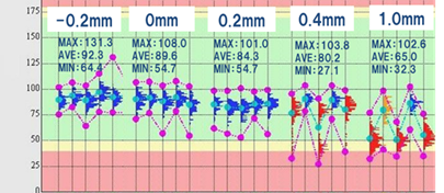
Figure 1. Stencil-to-board gap greater than 0.2mm compromises printing.
To establish a good enough seal, the maximum acceptable stencil-to-board gap is only 0.2mm. This limit becomes more critical than ever when printing for 0201mm. Statistical analysis of paste-volume repeatability at an aperture size of 0.22mm x 0.24mm shows how repeatability deteriorates rapidly as the stencil-to-board gap exceeds 0.2mm.
As the stencil gap becomes more critical, small details command more attention. The stencil frame must have enough rigidity to prevent excessive distortion when vacuum clamping is applied. Also, processes such as printing legends or barcodes with ink can cause unevenness. A possible solution is to use flexible stencils treated with a compliant material on the underside to enhance sealing.
With extremely small stencil aperture sizes, optimum filling efficient paste transfer after separation is critical.
Table 1. Paste types and major parameters.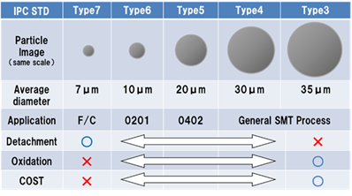
The squeegee angle is known to influence aperture filling more heavily than squeegee pressure and must be reduced as the paste roll diminishes. Experiment shows the squeegee angle should change from about 60° to 50° before paste is replenished. A servo-controlled head can automatically readjust the squeegee angle on each cycle.
The smaller 0201mm aperture area means solder paste particle size also becomes more critical. Currently, Type 3 and Type 4 pastes, with typical particle size of 30µm and 35µm, are used in general SMT assembly. Type 5 (20µm) pastes produce better results when printing for 0402mm chip-size parts but are more expensive.
A further reduction in particle size is needed to ensure repeatable printing on 0201mm-size pads. Type 6 paste with 10µm particle size is the obvious candidate but is about three times the price of Type 5. Blending powder sizes to create a Type 5.5 paste with 15µm average particles may offer a solution. Larger particles can also reduce oxidation and prevent reflow defects such as component detachment.
Table 2. Typical optimum stencil thickness for component sizes down to 0201mm.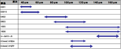
Stencil design has focused for many years on aspect ratio (aperture width ÷ stencil thickness) to achieve the best possible filling and transfer. A rule of thumb has specified a minimum ratio of 1.5, indicating reducing aperture sizes demands an associated reduction in stencil thickness. More recently, the area ratio (bottom area ÷ lateral area) has become a widely used metric, and experts have suggested a ratio of 0.6 or even 0.4 for the latest chip sizes.
To satisfy either of these formulas, the contact area of the pad must be greater than the total area of the aperture wall. Effectively, the stencil thickness must be reduced to ensure satisfactory paste release at smaller aperture sizes.
A stencil thin enough to print the minute volumes of paste for the smallest-size 0201mm pads will be unable to deposit adequate volume for larger parts. Stepped stencils have delivered limited success in overcoming similar, less severe, challenges in the past. Solder preforms can be placed where large volumes are required but are expensive and impose additional placement burden.
Figure 2. Large-volume and ultra-small paste deposits created using two-stage printing.
Yamaha has proposed two-stage sequential printing as a suitable solution. The smallest deposits are printed first, using the thinnest stencil. A thicker stencil is subsequently used to deposit larger paste volumes if required. The underside is routed to prevent contact with the existing solder deposits. A dual-lane printer with sequential printing mode is needed.
An additional benefit of sequential printing is the opportunity to reduce the solder-paste cost-per-board by using the more expensive type 5.5 or 6 paste for printing fine features only. A coarser particle size can be used for depositing larger volumes of paste.


Press Releases
- Kurtz Ersa Partners with E-tronix for Sales in Illinois and Wisconsin
- XLR8 EMS Welcomes Raul Jorge Lopez Jr. as Director of Program Management and Procurement
- Koh Young America Promotes Ramiro Mora to Lead Service and Applications in Mexico and South America
- ViTrox Americas Welcomes Huy Pham as Technical Support Engineer