Open Solder Joints on BTCs
 Measure changes in package dimensions during NPI.
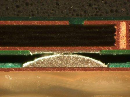
The open solder joint on this BTC area array package was caused by poor paste volume control. The solder volume was not sufficient to create a joint. As there was evidence of solder wetting on the component pad, the device was in contact with the paste during initial reflow. It is assumed the wetting to the PCB pad was faster than the component termination, which is the reason for the separation.
Variability in the solder volume on multiple pads may have caused the package to tilt and float, leading to separation. A high level of volatility during reflow also may have contributed to the open joint.
On some packages, warping during reflow can lead to opens. Measuring the change in dimensions of a package should be conducted during NPI, or better, before the component is considered in new designs.
These are typical defects shown in the National Physical Laboratory’s interactive assembly and soldering defects database. The database (http://defectsdatabase.npl.co.uk), available to all this publication’s readers, allows engineers to search and view countless defects and solutions, or to submit defects online. To complement the defect of the month, NPL features the Defect Video of the Month, presented online by Bob Willis. This describes over 20 different failure modes, many with video examples of the defect occurring in real time.

Figure 1. An open solder joint on a BTC.
is a consultant at the National Physical Laboratory (npl.co.uk); martin.wickham@npl.co.uk. His column appears monthly.


