

Lessons from 2011

The supply chain was hit hard in 2011. It’s unclear whether 2012 will bring a reprieve.
A cloudy global economic forecast is causing uncertainty among many corporations, even those in the electronics industry. While last year’s worries were caused by natural disasters, 2012 fears are manmade.
2011 was a year of natural disasters with countless lives lost and two major shocks to the electronics industry supply chain. Japan’s earthquake, tsunami and subsequent nuclear disaster shuttered some materials, equipment, silicon wafer, wafer fab, assembly operations, and final electronic product plants. It also exposed weaknesses in the IC package infrastructure, damaging companies with virtual monopolies that supply solder mask and resin used in IC package substrate production. One of the weakest links in the supply chain proved to be the supply of Bismaleimide Triazine (BT) resin used in IC package substrates. Mitsubishi Gas Chemical, the world’s largest supplier of BT resin, saw its plants in Iwate Prefecture impacted by the March 11 disaster. Some companies had qualified Hitachi Chemical’s E679, but supply of this material was also impacted by the disaster. Companies scrambled to qualify suppliers from other regions.
From one disaster to another. Japanese companies are major producers of materials used in semiconductor packaging and substrates, including IC package substrates, leadframes, bonding wire, mold compounds and encapsulants, solder balls, underfill and dielectric materials. As a result of the disaster, many companies began to examine their entire supply chains. MGC announced a new plant outside Japan, and in the long run, many Japanese companies will follow, permitting suppliers in other regions to gain some market share. Supply-chain disruptions from the earthquake and tsunami have been mitigated, but traditional price declines for many substrates did not take place in 2011. In some cases, there were price increases. With continued price pressures in 2012, companies will experience lower margins, unless production efficiency improvements can be realized.
Unprecedented flooding in Thailand resulted in not only human tragedy – almost 400 lives lost and more than 2 million disrupted – but also economic consequences. Economic growth was set back, and global electronics supply chains were again disrupted. Hard disk drive (HDD) producers and subassembly suppliers were flooded, and equipment will need to be replaced. In addition, some IC assembly facilities, automotive plants and related suppliers also suffered flood damage. PC shipments, especially notebook computers, have slowed.
The growing complexity of the supply chain itself, coupled with the increasing choice of technologies, makes it impossible to fully optimize packaging choices and understand cost tradeoffs without modeling supply-chain cost structures and capabilities. Many companies will spend greater resources on such analysis in 2012.
Europe’s financial woes. While Europe’s financial crisis put many corporations’ decision-making on hold, some US economic improvements have been seen. Unemployment rates have declined and consumer confidence improved. The fear is that Europe’s debt crisis will cause a credit squeeze that could cause the world economy to slump. The deteriorating situation in the Euro zone prompted the Organization for Economic Cooperation and Development to lower its growth projections for the US economy to 2% next year, down from its May forecast of 3.1%. It also lowered its economic outlook for Europe and the rest of the world. A credit contraction could exacerbate the slowdown.1 Manufacturing activity in China shrank in November for the first time in nearly three years.2 China’s labor unrest and real estate bubble are still cause for concern, but there is hope that the second half could see improvement, if solutions can be found for the financial situation and China is able to stimulate domestic growth.
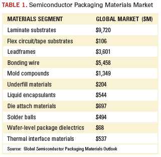
Higher raw material prices. The new Global Semiconductor Packaging Materials Outlook points to strong growth in laminate substrates, underfill materials, copper bonding wire, leadframe CSPs, and other areas (Table 1). In part, rising metal prices drive revenue growth. Given the high price of gold, copper wire bonding adoption will continue this year.
Fan-out vs. fan-in? With increased use of wafer level packages (WLPs) in smartphones and tablets, strong growth in unit shipments continues. WLP adoption is driven by increased demand for a thin, low-profile packaging solution, but with increased I/O counts and die sizes, some companies are considering use of a fan-out package. In the fan-out process, singulated die are placed into a “reconstituted wafer” with enough space around each chip to accommodate second-level connections. Other companies plan to go to finer pitch (0.3 or 0.35mm pitch) to continue use of conventional fan-in technology. The year will see these two options battle it out for the space on the mobile device board.
Packaging continues to move in the Z direction. The advantage of stacking chips vertically in a single package is increased functionality in a given area and package footprint. 3D through silicon via (TSV) technology remains one of the hottest topics. There is no question that 3D TSV will be adopted, but the timing for mass production depends on how the cost of the new technology compares with that of existing technologies and how quickly manufacturing issues are resolved. Typically the driver is high bandwidth between memory and processor and the need for lower power. The industry is clearly focused on solving problems associated with improving yield and lower cost. Many standardization efforts are underway. Stacked memory using TSVs is expected to be introduced by several memory makers. Elpida, Samsung, Micron, Toshiba and others are in various stages of devising TSV-based 3D chips.
Also, 3D versions of package stacking such as package-on-package (PoP) can handle logics issues such as memory procurement for different suppliers, and test issues.
Smartphones, tablet computers and other mobile communication devices will drive future advanced packaging requirements. While today’s WLPs, PoPs, and stacked die CSPs will remain popular, new versions of advanced packages are expected to emerge. As companies move from R&D into production, the difficult work is underway to address 3D TSV issues of design, thermal management, test and assembly.
References
1. E. Dash and N.D. Schwartz, “Crisis in Europe Tightens Credit across the Globe,” The New York Times, Nov. 29, 2011.
2. N. Winning and N. Brereton-Fukui, “Weak Manufacturing in Euro Zone, China Darkens Global Outlook, The Wall Street Journal, Dec. 1, 2011.
E. Jan Vardaman is president of TechSearch International (techsearchinc.com); jan@techsearchinc.com. Her column appears bimonthly.


