ABCs of Writing a Custom Boundary Scan Test

Sample vectors and code for expanding test coverage.
Boundary scan or JTAG (Joint Test Action Group) is an IEEE Standard 1149.1 that defines the test access port and boundary scan architecture of digital integrated circuits. Boundary scan is a test technique that involves devices designed with shift registers placed between each device pin and the internal logic (FIGURE 1). Each shift register is called a boundary scan cell. These boundary scan cells allow control and observation of what happens at each input and output pin. When these cells are connected together, they form a data register chain called the boundary register.
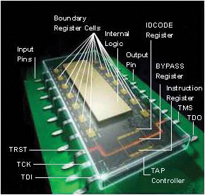
Figure 1. A boundary scan device.
Boundary scan has become an important limited access solution for printed circuit board assemblies, and includes tests for digital integrated circuits interconnection, as well as testing and programming digital devices such as flash, EEPROM and serial peripheral interface (SPI) devices. Boundary scan also has the capability to execute other tests, as defined in the BSDL (Boundary Scan Description Language), including private instructions which support internal functions of a boundary scan device, such as built-in self-test (BIST).
The boundary scan operation is controlled by a test access port (TAP), the control system of a boundary scan device. The TAP controller of a boundary scan device consists of a 16-state machine (FIGURE 2). The flow of data to the instruction register (IR) and the data register (DR) is controlled by the test mode select (TMS) with a 0 or 1 bit to move from one state to another state, while the TCK synchronizes the 16-state machine operation. The TAP controller state diagram shows the sequence of any boundary scan test through the TAP controller, and applies to components that comply with IEEE 1149.1.
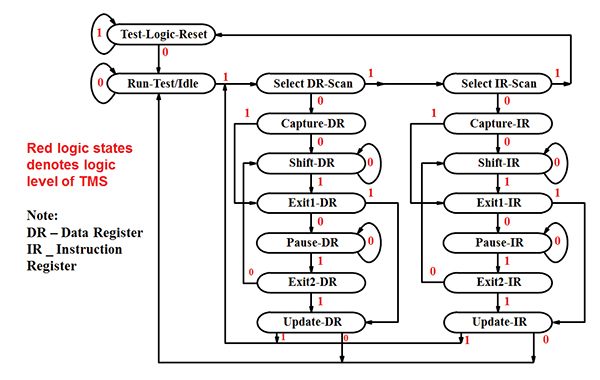
Figure 2. Test access port (TAP) state diagram.
Each position in the DR and IR columns represents a state of the TAP controller of the 16-state machine that controls each boundary scan device. The DR column comprises data instructions that, when passed through, affect the operation and contents of the data register. The DRs include bypass register, a mandatory register that all boundary-scan-compliant devices must contain. Either that or it will need to have the optional IDCODE, USERCODE registers, or a designer-specified register that complies with the IEEE standard.
The IR column comprises data instructions that, when passed through, affect the operation and contents of the IR, a mandatory component of every boundary scan device.
The success of boundary scan in the manufacturing test environment depends largely on the availability of ATPG (Automatic Test Program Generation), which can help test engineers develop and generate the boundary scan tests (Figure 2).
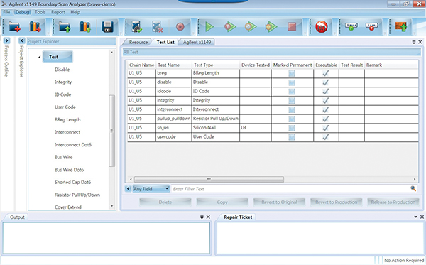
Figure 3. Boundary scan software interface with a built-in ATPG (Automated Test Program Generator).
The following are examples of automatically-generated boundary scan tests:
- Infrastructure test – Verifies that the TAP of all boundary scan devices in the chain operate properly. If this test fails, testing stops and power is disabled from the board. This test is a preamble to all other boundary scan tests; it is an integral part of each test and is executed before each test runs.
- Interconnect test – Verifies the boundary scan device pins 1149.1 and 1149.6 interconnection with other boundary scan device pins.
- Buswire test – The bus wire test looks for opens on all the bussed boundary scan devices that are not tested by the interconnect test. The boundary scan driver pins are tested one at a time to ensure all possible opens are tested.
- Pull-up/pull-down resistor test – This test determines if the pull-up or pull-down resistors connected to boundary scan pins are installed. It also verifies if the resistor is shorted or open.
- Cover-Extend test - A hybrid between vectorless test and boundary scan, enabling testing of connectors and non-boundary scan devices.
- Silicon Nail test – The boundary scan cell (driver/receiver) of the boundary scan device connected to the non-boundary scan digital device pins simulates the operation of the non-boundary scan device.
- CPLD/FPGA programming – Programming CPLD and FPGA devices.
- Programmable memory device test (NOR parallel flash, SPI, I2C, NAND Flash, etc.) – Programming the memory devices with static and/or dynamic data.
Writing a custom boundary scan test. Although the ATPG enables automatic generation of required boundary scan tests, there are cases when a test needs to be manually created. To understand the creation of a custom boundary scan test, it is easier to start with a simple boundary scan test. FIGURE 4 shows a boundary scan chain consisting of U1, U2 and U5 boundary scan devices. To test the connection between the boundary scan devices in the chain, the mandatory bypass instruction is executed on U1 and U2, while IDCODE is executed on U5, which verifies that the TDI and TDO of the boundary scan devices are connected together. This is in addition to the optional IDCODE, which verifies the U5 version, part number and manufacturer identification number.
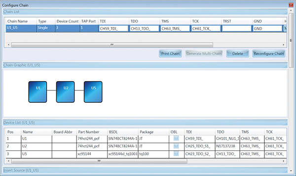
Figure 4. Boundary scan chain (U1, U2, and U5).
To manually generate the simple bypass and IDCODE test on the U1, U2 and U5 chain, a software language is needed to execute the TDI, TCK, TMS and TDO signals to simulate the state machine operation. Below is a sample of PCF (pattern capture format) vectors for U1 bypass only:
pcf order default Scan is TCK, TMS, TDI, TDO
!Column-to-Node Map, Nodes 1 to 4
!TTTT!
!CMDD!
!KSIO!
unit “IDCODE” ! Vector 1
pcf
use pcf order Scan
“01ZX”
“11ZX” !1st clock
“01ZX”
“11ZX” !2nd clock
“01ZX”
“11ZX” !3rd clock
“01ZX”
“11ZX” !4th clock
“01ZX”
“11ZX” !5th clock
“01ZX”
“11ZX”!Test-Logic-Reset
“00ZX”
“10ZX”!Run-Test/Idle - TMS is low
“01ZX”!
“11ZX”!Select-DR-Scan
“01ZX”
“11ZX”!Select-IR-Scan
“00ZX”
“10ZX”!Capture-IR
“00ZX”
“10ZX”!Shift-IR
end pcf
message “IEEE Std 1149.1-2001 Integrity Failure”
message “ Device U1 has failed,”
message “ suspect device or these pins:”
message “ (tck) 26”
message “ (tms) 27”
message “ (tdi) 34”
message “ (tdo) 35”
message “ (trst) 25”
pcf
use pcf order Scan
“000H”!0+0
“100X”
“001L”!1 IR loaded 01 @ TDO
“101X”
! Loading device U1 with instruction BYPASS(11111111)- 8 bit.
“001X”!2+0
“101X”
“001X”!1
“101X”
“001X”!2
“101X”
“001X”!3
“101X”
“001X”!4
“101X”
“001X”!5 Vector 50
“101X”
“001X”!6
“100X”
end pcf
message “IEEE Std 1149.1-2001 Integrity Failure”
message “ Device U1 has failed,”
message “ suspect device or these pins:”
message “ (tck) 26”
message “ (tms) 27”
message “ (tdi) 34”
message “ (tdo) 35”
message “ (trst) 25”
“000H”!7 !U2 loaded with IR 01 @ TDO
“100X”
“000L”!8
“100X”
The PCF vectors will need to have all the bits for the TAP signals (TCK, TMS, TDI and TDO) inputted to create a test. For a simple test like bypass, it is still possible to manually enter them. However, if the chain becomes longer, it is almost next to impossible to manually enter them, even for a simple test like bypass. To ease the creation of custom tests, some software interfaces support an SVF/STAPL-like language to help the user write their own custom test. Below is a custom test written in a custom language that simplifies the PCF vectors written above for U1 bypass:
ABSIR CAPTURE “U1” INST(BYPASS) COMPARE;
ABSDR CAPTURE “U1” DATA(#1) COMPARE(#0)
The rest of the state machine from Test-Logic-Reset, Run-Test-Idle, Select-DR-Scan, Select-IR-Scan, Capture-IR is executed automatically by the software that supports the custom language, which also synchronizes all the TAP signals (TCK, TMS, TDI and TDO).
FIGURE 5 shows an interface that supports custom language that a user will be able to write. In the custom insert source example are various instruction “opcodes” supported by the U1 BSDL, in this case for a Texas Instrument SN74BCT8244A.
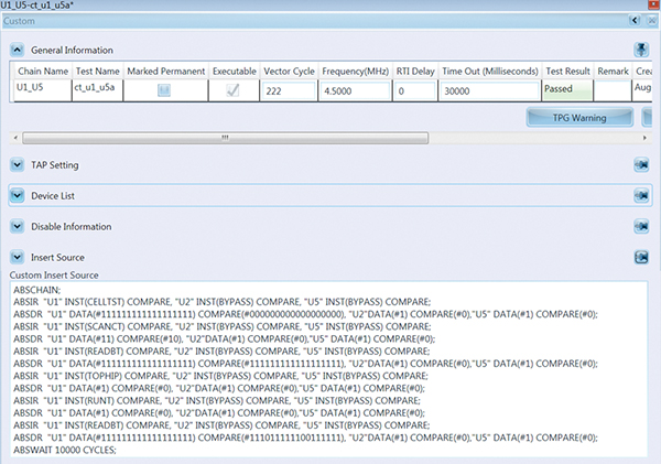
Figure 5. Interface that supports the execution of custom test.
The TI SN74BCT8244A BSDL file listed the following instruction opcode:
----------------------------------------------------
attribute INSTRUCTION_OPCODE of sn74bct8244a : entity is
“EXTEST (00000000, 10000000), “ &
“BYPASS (11111111, 10000100, 00000101, 10001000, 00000001), “ &
“SAMPLE (00000010, 10000010), “ &
“INTEST (00000011, 10000011), “ &
“HIGHZ (00000110, 10000110), “ & -- Bypass with outputs high-z
“CLAMP (00000111, 10000111), “ & -- Bypass with bs value
“RUNT (00001001, 10001001), “ & -- Boundary run test
“READBN (00001010, 10001010), “ & -- Boundary read normal mode
“READBT (00001011, 10001011), “ & -- Boundary read test mode
“CELLTST (00001100, 10001100), “ & -- Boundary selftest normal mode
“TOPHIP (00001101, 10001101), “ & -- Boundary toggle out test mode
“SCANCN (00001110, 10001110), “ & -- BCR scan normal mode
“SCANCT (00001111, 10001111) “ ; -- BCR scan test mode
------------------------------------------------------------------------------------
The manually-written custom test makes use of various test modes:
- CELLTST – boundary scan self-test normal mode.
- SCANCT – Boundary cell register (BCR) scant test mode.
- READBT – Boundary read test mode.
- TOPHIP – Boundary toggle out test mode, and
- RUNT – Boundary run test, which is not supported by the automatic test program generation.
FIGURE 6 shows the TDI signal waveform, expected TDO and actual waveform. The waveform graphics also show the device information, which includes either the hexadecimal or binary instruction. The user will also be able to navigate to the scan IR capture and DR capture executed during the test.

Figure 6. Waveform viewer showing the TDI, expected TDO and actual TDO of the custom test.
With the advancement of boundary scan software that supports simplified ISL, it is easier for test engineers to write custom tests to further expand test coverage. This is especially useful when implementing manufacturing tests on PCBAs with limited access, such as by using BIST, or when high-speed tests are required to test memory devices such as DDRs connected to a boundary scan device.
is a technical marketing engineer at Keysight Technologies (keysight.com); jun_balangue@keysight.com. The former Agilent Technologies Electronic Measurement Group is now Keysight.
Press Releases
- Nordson Test & Inspection Announces Strategic Partnership with Quiptech Mexico to Expand Market Presence
- Express Manufacturing, Inc. Expands Inspection Capabilities with Its Second TRI 3D AXI System
- Javad EMS to Add New ESPEC Temperature Chamber to Support Growing Mil/Aero Work
- ubersmt Builds Out SMT Line with Promation PCB Handling Equipment


