

Testing a Network Communication PCBA from Prototype to Manufacturing

The network communication (netcomm) printed circuit board assembly is one the largest boards in terms of size, number of nodes/nets and components. It also has the most advanced technology in terms of speed and complexity. The quality of a product and its success depends on deploying an effective manufacturing test strategy to catch structural defects and prevent bad boards from flowing down to the functional station, box build or, at worst, into customers’ hands.
The manufacturing process of netcomm PCBAs faces many test challenges, mainly due to the loss of test access (FIGURE 1) with the prevalence of the following technologies:
- Low voltage differential signal (LVDS) or high-speed differential signal.
- Increased usage of on-board memories (DDR).
- Multi-core processors.
- High-density interconnect (HDI) PCBs.
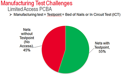
Figure 1. Manufacturing test accessibility of a typical netcomm PCBA.
Boundary scan is an important strategy to recover test coverage for netcomm boards during manufacturing test. Below are the following IEEE standards and boundary scan test system features that enable test engineers to recover manufacturing test (FIGURE 2):
1. IEEE Std. 1149.1. IEEE Std. 1149.1, the IEEE Standard for Test Access Port and Boundary-Scan Architecture, is the foundation of the boundary scan standard that enables testing of the interconnect between two or more boundary scan devices. Test features enabled on 1149.1 are:
- Infrastructure test (integrity, IDCODE, boundary register length).
- Interconnect test, which tests the connection between two or more boundary scan devices.
- Silicon Nails.
- Autobank, which enables silicon nails to test memories in a group or bank. The test time is significantly reduced. See below:
PCBA with 18 DDR3 memories on board.
Test time for each silicon nail for DDR3 = 9 sec.
Total silicon nails test time = 162 sec.
Autobank (Group of 9 DDR3) = 9 sec.
Total Autobank = 18 sec.
- Cover-Extend Technology, which tests non-boundary scan devices such as connectors or digital devices using boundary scan.
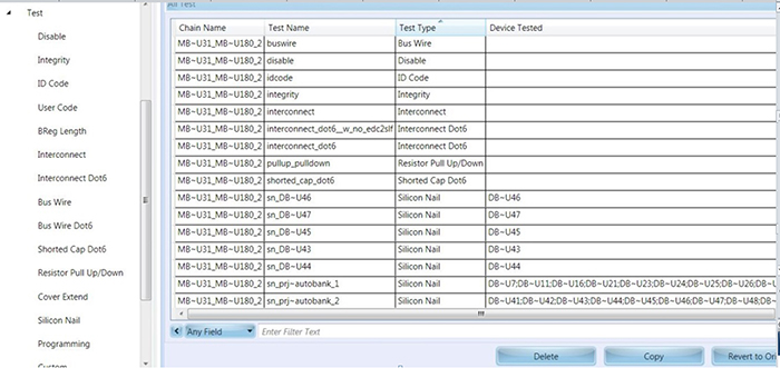
Figure 2. Boundary scan test.
2. IEEE Std 1149.6. IEEE Standard for boundary scan testing of advanced digital networks covers the differential signal (LVDS). The following tests are generated using 1149.6 standard:
- 1149.6 interconnect test, which tests differential connections between two or more boundary scan devices.
- Shorted capacitor test, which captures differential signals of shorted capacitor (AC coupling) between two boundary scan devices.
- Cover-Extend.
Boundary scan is cost-effective because it can be integrated into every stage of the PCBA manufacturing testing to recover coverage for those nodes/nets that have no test access, while at the same time reducing manufacturing test cost.
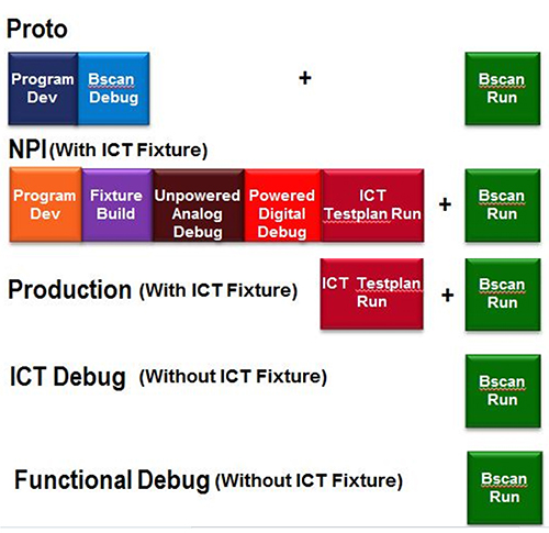
Figure 3. Boundary scan implementation for netcomm production.
Now let’s look at how a typical netcomm board is built, as it will give us a good idea on the test requirements and potential solutions:
1. Prototype build. This is the initial step where the design center or R&D team builds the board to verify software and hardware design.
Boundary scan test program development can be developed at the early stage of board development where only limited information is available, such as the netlist, bill of materials (BoM) and boundary scan description language (BSDL) of boundary scan devices. The test engineer will be able to feed back to the board design engineer any necessary changes to the board before fabrication that will enable BST and maximize test coverage during manufacturing testing. The following boundary scan design for test can be captured during program development:
- Availability of test access to the boundary scan chain test access port (TAP).
- Proper logic level of boundary scan compliance pins.
- Identify boundary scan chain to maximize coverage.
- Boundary scan interconnect (1149.1 and 1149.6) coverage.
- Proper fan-out of TAP pins for boundary scan test stability during testing.
- Identify non-boundary scan devices that can be tested.
- Verify boundary scan devices’ BSDL during testing.
2. New product introduction. This step involves a lot of work toward testing boards and verifying their manufacturability. Boards that are built will then be shipped to various sites of the company, or to customer sites and government bodies for certification and testing.
During the NPI stage, the in-circuit test (ICT) fixture will be fabricated to ready it for production testing. Integration and implementation of boundary scan from prototype to ICT will significantly reduce cost on test program development, and debugging of boundary scan tests is performed during the prototype stage. Also during the prototype stage, boundary scan issues can be found early and resolved before progressing onto the building of ICT fixture at NPI.
Typical netcomm nodes/nets can range from 6,000 to more than 10,000 per board. A PCBA designed for BST will be able to test at least 40% of these nodes, thus reducing ICT fixture and system requirements.
An obvious benefit is the lower cost of ICT fixtures. Nodes/nets tested identified and verified during prototyping by boundary scan can be removed from the ICT fixture. This will translate to significant cost-reduction for fabrication of the ICT fixture.
TABLE 1 shows an example of ICT cost-reduction. Note that in this case study, we assume each ICT test access removal can be translated to a $3 cost-reduction. Also note that costs are estimated and may vary by vendor and geography. In such a scenario, the loading on the ICT system resources will be reduced significantly, hence allowing manufacturers to use their existing production systems instead of buying a larger node count ICT system that will increase their manufacturing cost.
Table 1. ICT Cost Savings Using BST from Prototype through Production Test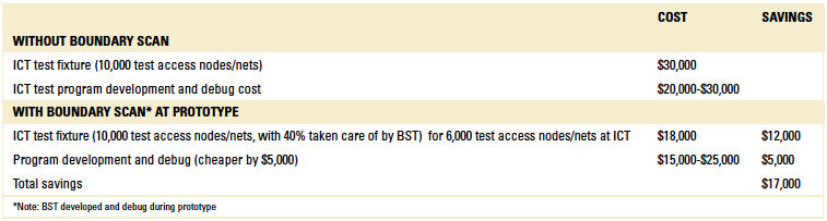
3. Production. The final step of the cycle is just before product starts shipping to customers. During the production stage, the BST developed at the early prototype stage can be integrated into the production stage for ICT, and can also be used as a debug station at both ICT and functional test.
Implementing a BST strategy for a netcomm PCBA during the prototype stage will not only ensure higher test coverage during prototyping, but also ensure NPI and production testing can more seamlessly accommodate the boundary scan test as production ramps up. A well-thought-out implementation strategy will thus not only ensure higher product quality, but also greatly reduce the cost of test for each netcomm PCBA produced.
is a technical marketing engineer at Keysight Technologies (keysight.com); jun_balangue@keysight.com.


Press Releases
- Altus Adds LPKF CuttingMaster 3290 to Depaneling Portfolio
- Kurtz Ersa Partners with E-tronix for Sales in Illinois and Wisconsin
- XLR8 EMS Welcomes Raul Jorge Lopez Jr. as Director of Program Management and Procurement
- Koh Young America Promotes Ramiro Mora to Lead Service and Applications in Mexico and South America