

PoP: 2 Times the BGAs, 2 Times the Problems?
 There are more solder balls to inspect, so use oblique views.
With board area often at a premium in today’s sophisticated and high-performance electronics, using the third dimension of height to enable greater device functionality is ever more attractive. In particular, package-on-package (PoP) devices have been around for years and are popular for this purpose. From an x-ray inspection point-of-view, the most common POPs can be considered as two BGAs stacked on top of each other. Therefore, the real and “virtual” issues associated with BGAs, as mentioned in previous columns, also come into play for these devices.
However, we now have an additional dimension (sic) to consider in the features seen in the x-ray images, as well as just having a single BGA and anything within, or on the second side of, the board. On top of these, we also have the potential for overlap of solder balls from the two BGA layers (FIGURES 1 and 2). As with BGAs, all the interconnections are underneath the package, and are not visible optically, permitting x-ray the opportunity to make nondestructive inspection analysis. With twice the number of BGAs in the same place, does this mean twice the number of potential problems or more?
Possibly!
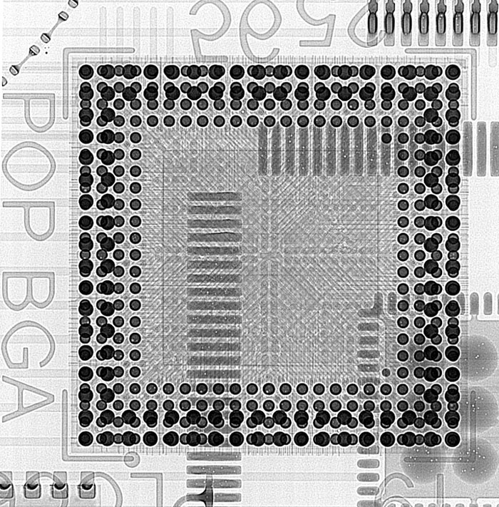
Figure 1. Top-down x-ray image of package-on-package (PoP) device.
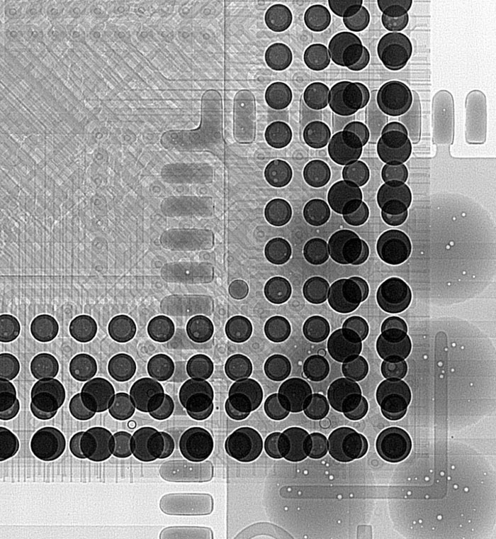
Figure 2. Magnified top-down x-ray image of a small area within the PoP seen in Figure 1. The overlap of the two BGA interconnection layers is clearly visible.
The same x-ray inspection criteria for PoPs apply as for single BGAs. Initially, try to look from the top down for anything obvious, such as missing balls and excessive voiding in either “BGA layer.” Figure 2 shows a missing solder ball on the inner corner pad, as the diameter density is much smaller than neighboring joints, but in this case, this is probably by design rather than omission. FIGURE 3 shows more typical views of what missing solder balls can look like. This is from a BGA, not a PoP, but is included to highlight the differences more clearly. Obviously, the overlapping solder balls from the two BGA layers in Figure 1 and 2 make acceptable fault analysis more difficult for even a simple top-down view of PoPs. Therefore, taking oblique angle views of PoPs becomes more important, not just for joint quality verification but also to separate the different layers of solder balls to help with the analysis.
Figure 3. Top-down x-ray image of BGA with missing solder balls in the center and at the bottom left corner.
This is also why the use of partial CT, or limited angle CT (articles passim), if available on your x-ray system, is also very helpful for PoP device analysis, as it will allow the different layers within to be analyzed independently, without the clutter of other levels in the same field-of-view. Missing balls and overlarge voids will stand out clearly and also help confirm at which level(s) the problem(s) is occurring.
When interpreting PoP images, remember my old friend the geometric magnification of the x-ray system will potentially make the solder balls appear as different sizes at the two BGA layers, even when the solder balls themselves may be the same diameter throughout the device. This effect will be greater at higher magnifications. (See the relative ball diameter differences in the two layers in Figures 1 and 2.) This is caused by the solder ball layer closer to the x-ray tube projecting a larger shadow at the detector, compared with the layer of solder balls farther away. Overall, for PoP inspection and standard BGAs, look for variation and differences within the solder balls of the same layer, rather than compare the BGA layers with each other. This is true for PoPs and for inspecting newer 3-D package types increasingly used.
POPs: two times the problem of BGAs? Certainly there are more solder balls to check, and the configuration adds complexity to the images from which we have to deconstruct the faults, but taking a systematic approach to the analysis, using more oblique views and partial CT (if available) should allow ready confirmation of the joint quality and tame these beasts!
Au.: Images courtesy Peter Koch, Yxlon International.
, is an expert in use and analysis of 2D and 3D (CT) x-ray inspection techniques for electronics; dbc@bernard.abel.co.uk.


Press Releases
- Green Circuits Announces Strategic Partnership with Metatron Private Equity
- Smartsol Technologies Mexico Strengthens its X-ray Division and Announces Strategic Partnership Expansion with Creative Electron
- Hanwha Semitech Americas Supports Regal Technology Partners with New SMT Line Installation
- AIM Hires Marcus Pee as Sales Engineer for Southeast Asia