

QFN Inspection: Don’t Forget the Edge!
 Voiding under edge terminations is often overlooked, to the detriment of yields.
My last column focused on voiding under QFNs. Primarily, this concentrated on voiding under the central termination. As I discussed, the potential for voiding in this area is high, owing to the limited available escape pathways to remove outgassing volatiles created during reflow from under the center of these planar objects. This can result in the often-typical voiding issues that are usually clearly seen in their x-ray images. Therefore, this can then be the natural and easy focus for an operator to concentrate on as the location of the likely fault or failure, even if the “substantial” level of voiding may be acceptable from a supplier and customer point-of-view. With voiding (when present) usually being so obvious, yet probably at an acceptable level, once the central termination has been considered and passed by the operator, then the edge terminations may not then be fully considered, or possibly even ignored completely, as the potential source of problems. Therefore, I would like to present some images of good and bad QFN edge terminations to highlight some of the features that may be seen in the x-ray images to indicate the problem could be at the edge and not in the center.
As with all x-ray analysis of solder joints, the best methodology to find flaws is to look for variations across similar features. If there is consistency in the feature shapes, and unless you are very unlucky and have 100% of the joints failing, then with experience it should be more straightforward to identify failures. By being a planar device, however, QFN edge terminations have far less solder volume than BGA joints, and the opportunity for more obvious variations may be reduced. Therefore, higher magnification and oblique angle x-ray views may be necessary to confirm an issue. Of course, don’t forget to look (and measure if required) at the level of voiding in the edge terminations as well!
As an example, consider the QFN in FIGURE 1. This is a very “good bad” sample to illustrate my point. QFN joint differences on real boards may be subtler than that shown. In this case, though, ignore the central termination where solder may not have been placed in this sample and look at the edge terminations. There appears to be consistency over most of the joints, with the exception of some on the righthand side. A cursory glance at this level of magnification may be sufficient to spot the difference and raise the alarm, but to the less-trained eye the differences are minor and could be easily overlooked. Therefore, taking the time to make higher magnification views on QFNs is worthwhile, as the top-down, magnified view of the bottom right corner of this QFN shows (FIGURE 2). The joint variations are much clearer. There are darker joints and lighter ones. But which are the soldered ones?
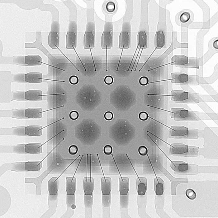
Figure 1. Top-down x-ray image of QFN with variable edge termination consistency.
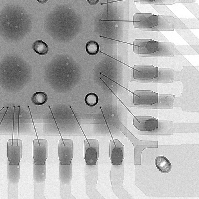
Figure 2. Top-down magnified x-ray image of QFN edge terminations in Figure 1.
More information can be gathered from the oblique view (FIGURE 3). Perhaps surprisingly to some, the darker joints in Figure 3 are the soldered ones; the lighter joints show a complete absence of solder between the device and the pad. For this example, therefore, only eight of 28 joints actually have been made. Arguably, for this particularly extreme example, even the soldered joints may not be deemed to be acceptable, but it may help to identify not just the variations possible but also to remind that what might be initially considered “real” joints (the lighter ones) are actually not!
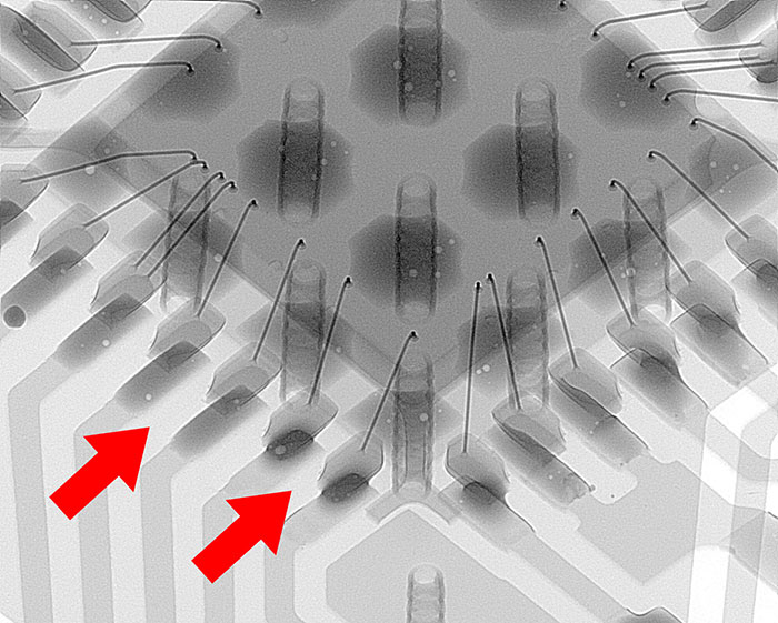
Figure 3. Oblique view x-ray image of QFN edge terminations. Highlighted joints show substantial shape variation indicating soldered and open joints.
Overall, when analyzing QFNs with x-ray, look at the central termination and consider (and measure?) the voiding level to ensure it lies within mutually agreed guidelines. However, don’t forget the edge terminations, and make magnified and oblique angle views to confirm all is well. Further, as QFN edge termination variability may be subtler than for other joint types, take and keep a library of reference images of known “good” and “bad” samples (if any!) of your actual boards. Real circuits are usually not single-sided like this example, and you will probably need to make any analysis against the overlap of second-side features. A reference image library of your boards provides not just a benchmarking exercise and resource to share, discuss and confirm quality issues with other interested parties and give confidence to your analysis on future samples, it also ensures you have a training aid to support and educate future operators.
Au.: Images courtesy Peter Koch, Yxlon International.
, is an expert in use and analysis of 2D and 3D (CT) x-ray inspection techniques for electronics; dbc@bernard.abel.co.uk.


Press Releases
- Altus Adds LPKF CuttingMaster 3290 to Depaneling Portfolio
- Kurtz Ersa Partners with E-tronix for Sales in Illinois and Wisconsin
- XLR8 EMS Welcomes Raul Jorge Lopez Jr. as Director of Program Management and Procurement
- Koh Young America Promotes Ramiro Mora to Lead Service and Applications in Mexico and South America