Wetting Indicators for BGAs
A few well-placed cues make “true” design-for-test.
I often hear the terms design for manufacture (DfM) and design for test (DfT) applied to board design. To be perhaps a little provocative, I would suggest there is much talk about both subjects, with some implementation for DfM, but very little for DfT. I recognize these opportunities may have cost, design and other implications, but these must be balanced against potential downstream costs associated with poor manufacture, test and long-term reliability. A case for consideration is the inclusion of wetting indicators under BGAs as a DfT.
Wetting indicators are where the reflowed joint is deliberately made into a different characteristic shape, when viewed in an x-ray image, compared to the shape of a typical or “standard” reflowed BGA joint. This can be achieved by incorporating a design change that permits the solder to wick slightly away from the joint location back down the pad during reflow. Such modifications can be made by either making the pad shape different from the other BGA joints or modifying the solder mask to add a small quantity of extra solder and extend the solder away from the joint. With both methods, solder reflow will result in a different joint shape compared to the typical BGA. I understand these changes do not affect joint quality and reliability. Nor is there need for all joints to be modified, perhaps just some at the center and edge of the device.
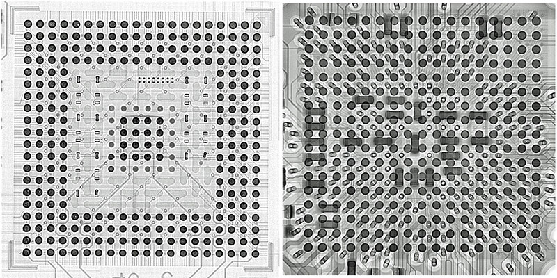
Wetting indicators provide a quick, easy x-ray visual check that reflow has taken place. This can be seen clearly at low magnification and from the top-down view, thereby not requiring oblique views. This can be particularly helpful when hundreds of solder balls in the device and second-side components overlap, and potentially confuse the analysis. Consider FIGURE 1, which shows x-ray images of two BGAs from the top-down at low magnification. All the joints look consistent, but there are many features to check. For the single-sided test board BGA (at left), this is difficult to do. Now add the confusion of the second-side components overlapping the BGA of a “real” board (on the right)! In these cases, additional x-ray views at higher magnification and oblique angles will be needed to provide confidence that reflow has taken place successfully. Wetting indicators give this confirmation at low magnification and in a single image. Note, however, just because we are confident reflow has taken place, we cannot assume every joint is okay. Additional checks should still be included.

Figure 1. Top down, low magnification x-ray images of BGAs.
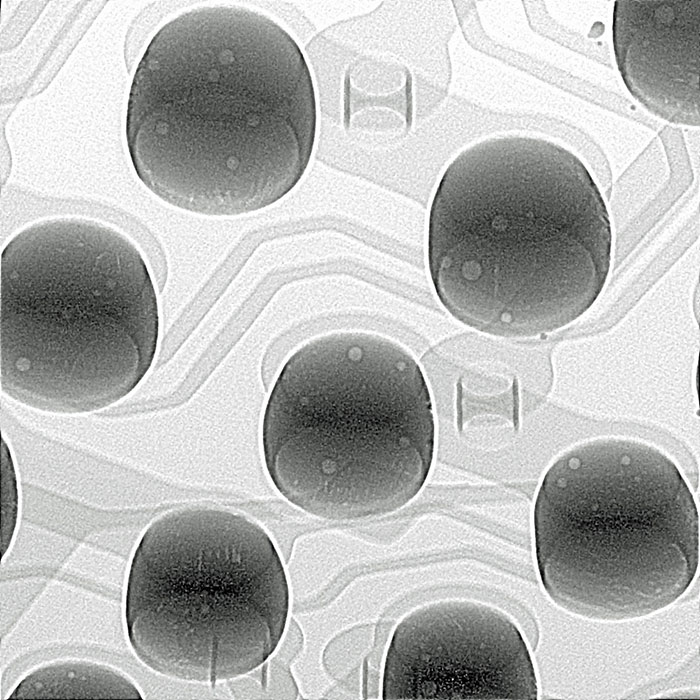
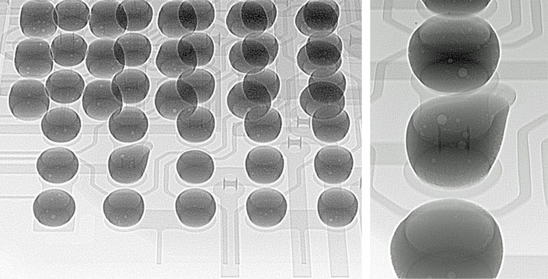
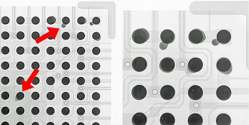
FIGURE 2 shows an oblique view x-ray image of correctly reflowed BGA solder joints. All are similar. FIGURE 3, in contrast, shows an equivalent oblique view but with one joint in that BGA including a wetting indicator. This is in the center of the image. A magnified view is shown on the right. The difference in the shape is clear. FIGURE 4 shows another low-magnification top-down x-ray view. The presence of the pad-defined wetting indicators in this case shows clearly that reflow has not taken place, at least in the top right of the device, as seen in the image. Compare this to the successfully reflowed wetting indicator in the center (highlighted). This correctly reflowed joint appears to have a subtle difference compared to the adjacent joints. Therefore, more distinct design approaches to the wetting indicator can be considered to improve how a correctly reflowed wetting indicator appears. Since we know where the wetting indicators have been placed, however, we know where to look for the correct joint(s) in our examination.

Figure 2. Oblique view x-ray image of reflowed BGA solder joints.

Figure 3. Oblique view x-ray image of BGA containing a successfully reflowed wetting indicator under a BGA. Magnified image is shown to
the right.

Figure 4. Top down x-ray images of BGA with reflow indicators included. Top right indicators show reflow has not taken place correctly and can be contrasted with the successfully wet indicator in the center.
With BGA joints being optically hidden, x-ray inspection is typically required to look for BGA problems. I have looked at BGAs often in this column and suggested approaches for better testing, as they are often the primary reason for investing in an x-ray system. I have also long advocated that, for best fault analysis, look for differences between equivalent joints. Perhaps it is time to use this to our advantage? The inclusion of wetting indicators under BGAs offers the ability to speed up testing by giving a quick indication that solder reflow has taken place correctly. In this way, assemblers can manufacture PCBA with more confidence, customers have added assurance that reflow has been successful, and certain issues can be ruled out if and when problems occur.
Au.: Images courtesy Peter Koch, Yxlon International.
, is an expert in use and analysis of 2-D and 3-D (CT) x-ray inspection techniques for electronics; dbc@bernard.abel.co.uk.


