Filled Out

Is via-in-pad a solution for dense flex boards?
Question: I just designed a flex circuit with six layers and very high density on the outer layers, which limits fan out. I have used via-in-pad on similar rigid designs, and it has worked very well. Can this strategy also be used on flex circuits?
Via-in-pad is a great tool to free some PCB real estate, but there are a few things to know about using this construction with flex. I assume that on the rigid design, vias in the SMT pads were filled with a nonconductive resin and then planarized. This leaves a really smooth surface for the assembler to work with and process normally. I would not go so far as to say via fill and planarization are easy on rigid PCBs, but I will say they are much easier on a rigid PCB than on flex. The biggest reason for the added difficulty is the uneven topography of a flex compared to a rigid PCB.
On rigid PCBs, vias are typically filled after the initial interconnect copper plating and before the final cap plating. At this point, a rigid panel is typically very smooth and planar, and the outer surfaces have almost no topography. Rigid laminates and prepregs used in rigid construction act to fill between internal etched features. The via fill operation usually involves a process similar to screen printing. Some fill material is always left on the surface of the panel where it is not wanted.
Unremoved, the residue will get plated over during cap plating and will result in an etch flaw when final etch is performed. To remove this unwanted residue, rigid PCB panels are run through a sanding machine that removes the hardened fill residue and also a small amount of surface copper. Since the surface of a rigid PCB is so flat, the amount of surface copper removed can be accurately regulated.
On a flex circuit, all the dielectrics and adhesives are very thin films. When a multilayer flex circuit panel is laminated, you can clearly see a lot of the circuitry from the internal layers embossed on the outer surface. This topography really throws a wrench in the works for a flex fabricator when filling vias. When fill material is applied to a flex panel, it fills the vias and also many of the low spots on the surface (e.g., between adjacent conductors). It is really difficult to remove hardened resin in the panel’s low areas without removing a lot, or all, of the surface copper in the “high” areas. As such, often operators must go over every single panel and scrape the excess resin in the low areas by hand with an Exacto knife or similar means. You can imagine how that will add to the cost of the flexible PCB.
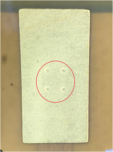
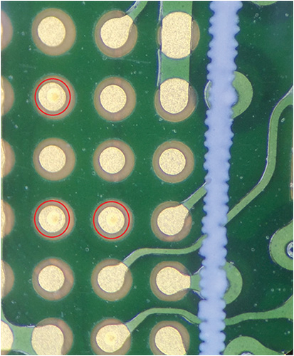
A more common strategy for using via-in-pad on multilayer flex is to fill the vias with copper plating. Many flex suppliers have special copper fill plating lines that will preferentially plate via holes and effectively fill them without adding a significant amount of plated copper on the panel surface. Excess surface copper plating can make it very difficult to define the very small features on the outer layers that typically go hand in hand with designs that require via-in-pad. Since vias are selectively plated with only copper and there is no resin fill, there is no need for a subsequent sanding operation; hence, the uneven topography of the flex circuit is a non-issue. The downside to this process is the “filled” vias are almost never completely filled. There is typically a very small dimple on the SMT pad surface where each via is located. On larger SMT pads (FIGURE 1) this is usually not an issue, but on very small pads such as 01005 chips and small BGAs (FIGURE 2) these dimples can pose challenges for the assembler. Sometimes the component assembler must modify their tools and processes to deal with the small depressions (e.g., adding slightly more solder paste to pads that contain a dimple).

Figure 1. Small dimples in larger SMT pads typically do not pose issues during component assembly due to the relatively small area they cover on the pad.

Figure 2. Small dimples on very small pads can cause some assembly headaches since the dimple occupies a large portion of the pad surface.
Everything I have covered to this point assumes multilayer flex. Rigid-flex can also utilize via-in-pad and, depending on the application and material stack, the fill method can vary by design. For instance, if the rigid cap layers on a rigid-flex are relatively thick (~0.010"+), they may be filled with resin and planarized like a rigid PCB. Thinner outer cap layers (0.003" or less) may use the copper fill option. For everything between 0.003" and 0.010", it is probably best to get your flex supplier’s input on the best option for your application.
is senior application engineer at Flexible Circuit Technologies (flexiblecircuit.com); mark.finstad@flexiblecircuit.com. He and co-“Flexpert” Nick Koop (nick.koop@ttmtech.com) welcome your suggestions.
Press Releases
- Flying Probe Testing: A Practical Solution for PCB Designs That Traditional Fixtures Cannot Test
- ubersmt Implements PARMI Xceed 3D AOI to Strengthen Inspection and Process Control
- Altus Group Expands Sales Support Function with New Appointment in Ireland
- Kitron Secures EUR 37M order for Next-Generation Tactical Communication Equipment


