

Maximizing High-Speed Performance in Flex Boards
 Flex circuits can run 10+Gb/s signals, but many factors need to be met.
Can flex circuit boards run 10+Gb/s signals? Answer: Multiple factors must be juggled to successfully run signals that are 1Gb/s and above on flexible circuitry. I will address each of them individually.
Controlled impedance. Just like any high-speed rigid PCB, a successful high-speed flex design will have to incorporate a target characteristic impedance. To do so, match the characteristic impedance of the flex to the rest of the system to ensure minimal reflections and crosstalk. This can have negative consequences for mechanical performance, however. Elevated impedance requirements typically equate to thicker dielectrics, thereby making the circuit much less flexible.
The impedance value of a circuit is driven primarily by the signal trace width, the layer-to-layer spacing between signal trace and reference plane, and the dielectric constant (Dk) of the insulating material between the signal and plane. For most flexible-circuit manufacturers, yields start to drop when trace widths fall much below 0.003" (0.0762mm), so any significant trace width reduction beyond that can have a hefty cost impact. Also, traces under 0.005" are fragile and may develop cracks in tight bend-radius applications.
If flexibility is a concern, raising the dielectric thickness between signal and plane layers is not a great option because of the additional stiffness it will create. The Dk of standard polyimide with thermosetting epoxy or acrylic adhesive ranges between 3.2 and 3.5, which is not great if the goal is elevated impedance combined with a circuit that will bend without breaking.
Many flex designers use a cross-hatch pattern for the reference plane(s) rather than solid copper (FIGURES 1-3). This trick will bump up impedance without the need to decrease signal trace width or increase dielectric thickness. The downside to using cross-hatched shields is increased insertion loss. Depending on how much loss the system can tolerate, this may or may not be feasible. If all the limits have already been pushed and higher impedance is still needed, consider some less-common insulating materials that have a lower Dk. Most of these materials also have lower insertion loss, which is a perfect segue to the next topic.

Figure 1. The most common cross-hatch pattern is a series of perpendicular traces forming a “screen” image. This pattern runs at 45° to the signal traces.
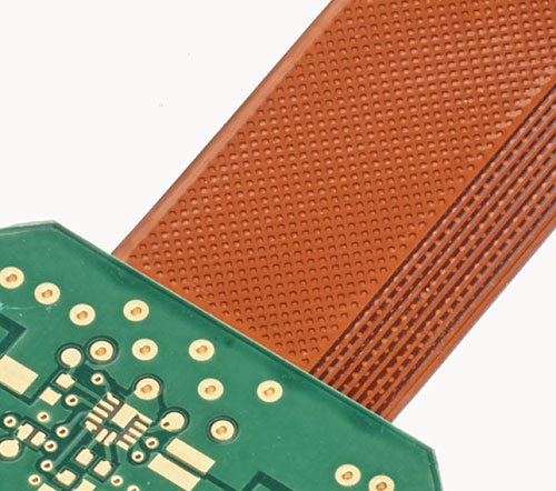
Figure 2. This image is a solid plane with round dots removed to provide a cross-hatch pattern.
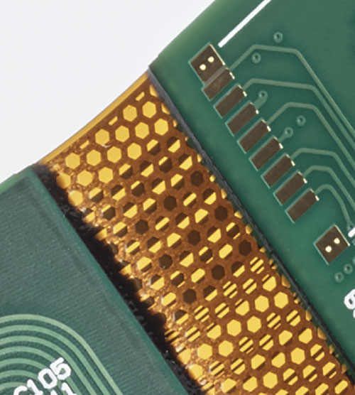
Figure 3. Honeycomb cross-hatch pattern.
Insertion loss. Most high-speed signals are very small and cannot afford to lose any amplitude on the way to their termination. And just like impedance mismatches can cause reflections that degrade small signals, high insertion loss materials surrounding the signal traces can eat up a lot of signal strength. Several available materials offer lower insertion loss, and at the same time lower Dk. Everyone wins, right? Well, sort of, but at a cost. Most of these materials are thermoplastics like Teflon and LCP (liquid crystal polymer), which are very expensive and not particularly easy to work with. Processing temperatures for laminating LCP and Teflon are upwards of 300°C. Since processing temperatures for laminating standard epoxy or acrylic adhesive are under 200°C, many flex manufacturers lack proper high-temperature lamination equipment required to run LCP or Teflon. This will reduce the potential vendor base.
Additionally, most high-speed materials have a propensity to be considerably more difficult to work with than standard epoxy- or acrylic-based flex materials. Unlike standard thermosetting adhesives, which cure and then stay put in subsequent laminations, thermoplastic high-speed adhesives can re-melt and permit features to move and shift if extreme care is not taken during additional lamination cycles. It’s easy to divine that the increased raw material cost, limited vendor base, and complicated processing will have a significant impact on final circuit cost. Some newer materials combine low Dk values and low insertion loss with lower lamination processing temperatures (very similar to epoxy and acrylic). While the newer raw materials are still more expensive than standard flex materials, the relative ease-of-processing can soften the blow on cost with improved yields and also a larger vendor base.
Rigid-flex considerations. Rigid-flex circuitry has additional concerns to be dealt with since any signal running from a rigid area, across a flex section, and back into a rigid area will travel through very different materials. Sensitive signals should be kept within individual rigid areas whenever possible. If signals must bridge a flex section, perform impedance calculations for both the flex and rigid areas, and adjust trace widths to provide matching values.
Ensure any conductor width changes occur on the rigid side of the flex-rigid transition, not on the flex side! A conductor width change on the flex side of the flex-rigid transition could result in a stress concentration point, which in turn could cause the trace to crack when the circuit is flexed. Discuss with your fabricator high-speed materials used in the rigid sections of the circuit. Not all high-speed rigid materials have a matching no-flow prepreg adhesive. No-flow prepregs are required in the construction of rigid-flex designs to ensure the prepreg does not flow into flex areas during lamination.
Terminations. At some point high-speed flex must be terminated with compatible connectors that can maintain an uninterrupted signal return path and also offer matched impedance. While most connectors designed to be mounted to rigid PCBs can also be mounted to flex, it is important to ensure any connector selected is compatible with flexible circuitry. And as always, it is wise to enlist input from the flex-circuit manufacturer on all these attributes early in the design process to ensure the final high-speed flex is both cost-effective and will perform as expected.
is senior application engineer at Flexible Circuit Technologies (flexiblecircuit.com); mark.finstad@flexiblecircuit.com. He and co-“Flexpert” (nick.koop@ttmtech.com) welcome your suggestions. The authors will speak on flex design and manufacture at PCB West in September (pcbwest.com).
Register now for PCB WEST, the largest trade show for the printed circuit and electronics industry in the Silicon Valley! Coming Sept. 11-13 to the Santa Clara Convention Center.


