2011 Issues
FEATURES
Cover Story
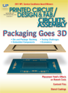
Benefits and Challenges of 3D Semiconductor Packaging
By integrating multiple die elements within a single package outline, overall product functionality has increased and been made smaller than their predecessors, improving both performance and capability. Assembly of semiconductor die onto a substrate is essentially the same as those used for standard IC packaging in lead frames; however, substrate-based IC packaging for 3D applications can adopt a wider range of materials, and several alternative processes may be used in their assembly.
by Vern Solberg
Component Placement
The Effect of Placement Yield on Rework Costs
Calculating rework and scrap cost is relatively straightforward, provided the production line’s first-pass yield is known. Knowing how pick-and-place accuracy can impact post-assembly costs, however, can be an invaluable benchmark, as this study of cost as a function of various yield rates and line capacity shows.
by Sjef van Gastel
Inspection
Using Automated SPI to Qualify SMT Stencil Suppliers
The goal of stencil printing can be summed in one simple phrase: Get the right amount of solder paste in the right spot – every time. And the right stencil starts with the right supplier, but with all the options in metals, manufacturing processes, frame styles and price, selecting a stencil vendor can be a considerable task.
by Chrys Shea
FIRST PERSON
- Caveat Lector
Standard problems.
Mike Buetow
MONEY MATTERS
-
ROI
Ensuring onshoring.
Peter Bigelow - Focus on Business
Talk, talk, talk.
Susan Mucha
TECH TALK
-
Technical Abstracts
In Case You Missed It.
FEATURES
PCB PROCUREMENT
10 Tips for Purchasing PCBs
Four industry veterans with backgrounds in PCB materials, chemistry, fabrication and assembly provided their expert advice, often echoing each other’s recommendations. If you want to maximize PCB quality, price, performance, delivery or overall value, try following some of these insiders’ tips.
by Marissa Oskarsen
CATCHING COUNTERFEITS
Verifying Component Authenticity Using Decapsulation
Decapsulation is a process that has been around for some time and has many different applications. Whether for analysis or verification purposes, the goal is the same: expose the die to perform the task at hand. While different methods are available to achieve this, manual etching has become a primary choice for exposing the die, as it leaves the device in question functional.
by Don Davis
FIXING THE FENCE
RF Shield Rework
RF shield rework is difficult due to continually shrinking package sizes, reduction of pitch and reduced clear space available around components. This increased density and complexity drives new techniques for removing and replacing RF shields. A new solution involves high-energy conduction heating and custom tips.
by Paul Wood
FIRST PERSON
- Caveat Lector
Martin’s law.
Mike Buetow
MONEY MATTERS
- Global Sourcing
Making sense of the macros.
Jennifer Read -
ROI
Taken for granted.
Peter Bigelow
TECH TALK
-
On the Forefront
Supply chain unlinked.
E. Jan Vardaman -
Process Doctor
Smaller and tighter heightens residues’ effects.
Dr. Mike Bixenman -
Materials World
Printed electronics applications.
Jie Bai -
Technical Abstracts
In Case You Missed It.
FEATURES
QA MODELING
Are Current Qualification Practices Adequate?
It is well known that devices and systems pass existing QT only to fail in the field. Other devices undergo extensive – and expensive – testing. Is this a problem? And do we truly understand the cost not just of failure, but of excessive test? A new approach to qualifying electronics devices could ensure a predictable, and low, probability of failure.
by Ephraim Suhir, Ph.D. and Ravi Mahajan, Ph.D.
SOLDER PROFILE
AIM Sets Its Targets
A family run business since 1936, AIM has become one of the world’s five largest electronics solder manufacturers. If only the world electronics industry knew. In an exclusive, Circuits Assembly goes inside the company's vast Montreal manufacturing facilities to find out what makes AIM at once so successful yet so unsung.
by Mike Buetow
SCREEN PRINTING
Testing the Mettle of Stencil Foils
According to our latest design of experiments, foil alloy does influence paste release: Over an area ratio range of approximately 0.5 to 0.75, the best performers were fine grain stainless steel and electropolished stainless steel.
by Chrys Shea
FIRST PERSON
- Caveat Lector
Hedging turmoil.
Mike Buetow
MONEY MATTERS
- Global Sourcing
No stopping Thailand or Tunisia.
Jennifer Read -
ROI
Productivity lost.
Peter Bigelow - Focus on Business
Building the EMS brand.
Susan Mucha
TECH TALK
-
Screen Printing
Understencil cleaning.
Clive Ashmore -
Tech Tips
The best tip(s).
ACI Technologies Inc. -
Test and Inspection
In-circuit’s direct savings.
Wee-Sheng Yong - Getting Lean
Customer involvement.
Steve Fraser -
Technical Abstracts
In Case You Missed It.
Press Releases
- Flying Probe Testing: A Practical Solution for PCB Designs That Traditional Fixtures Cannot Test
- ubersmt Implements PARMI Xceed 3D AOI to Strengthen Inspection and Process Control
- Altus Group Expands Sales Support Function with New Appointment in Ireland
- Kitron Secures EUR 37M order for Next-Generation Tactical Communication Equipment


