Plug Those Vias!

Via-in-pad soldering is prone to voiding, unless the vias are plugged and plated.
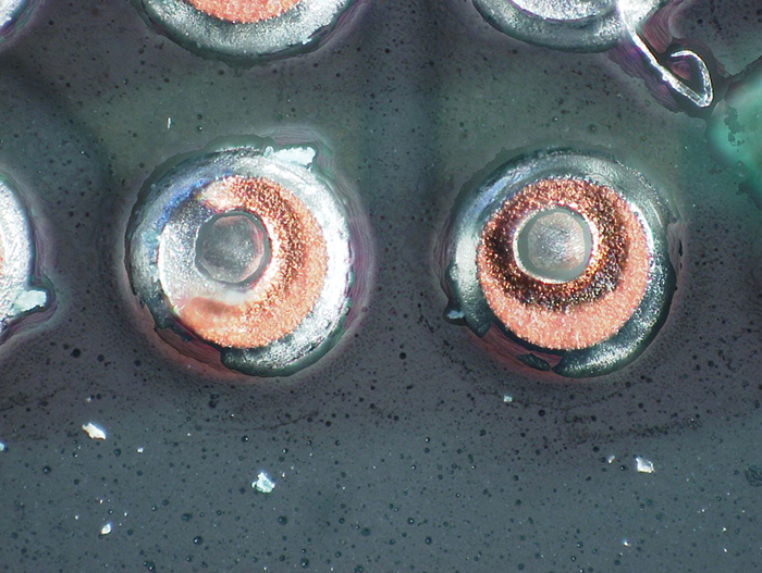
Via-in-pad will cause voids in solder joints unless the via is plugged, capped and then plated. If there is no outgassing during soldering from the board through the via plating or due to volatile material or air trapped in the cavity during printing, the issue can be avoided. Voids in joints, if excessive, can reduce the actual solder in contact with the pads on the board or the component pad, thus reducing the strength of the solder joint. We have seen very thin walls permit dye and pry indicator fluid to fill the void during testing.
Random gassing significantly increases the variation in solder joint size, lessening the value of ball size measurement as a process-monitoring technique for reflow and rework. Variation in ball size is a good, simple way to monitor process variation and package warpage. It is fair to say that, if shear force measurements are conducted on standard BGA pads and pads with via-in-pad with no voids, the force required to displace the via-in-pad joints is higher, but void-free soldering cannot be guaranteed.
These are typical defects shown in the National Physical Laboratory’s interactive assembly and soldering defects database. The database (http://defectsdatabase.npl.co.uk), available to all this publication’s readers, allows engineers to search and view countless defects and solutions, or to submit defects online. To complement the defect of the month, NPL features the “Defect Video of the Month,” presented online by Bob Willis. This describes over 20 different failure modes, many with video examples of the defect occurring in real time.

Figure 1. CSP balls with pads removed from via-in-pad board.
is with the National Physical Laboratory Industry and Innovation division (npl.co.uk); chris.hunt@npl.co.uk. His column appears monthly.
Press Releases
- Nordson Test & Inspection Announces Strategic Partnership with Quiptech Mexico to Expand Market Presence
- Express Manufacturing, Inc. Expands Inspection Capabilities with Its Second TRI 3D AXI System
- Javad EMS to Add New ESPEC Temperature Chamber to Support Growing Mil/Aero Work
- ubersmt Builds Out SMT Line with Promation PCB Handling Equipment


