

Can the Solder Stand the Heat?
 Too much heat during reflow can force solder out of a BTC.
FIGURE 1 shows examples of solder beads after reflowing bottom termination components (BTC). The beads are related to placement force prior to reflow, where the solder paste deposit is displaced away from the pads before reflow soldering. It is uncommon, but solder beads have also been seen coming from the package itself due to excessive heat during reflow. Solder beads or balls on the side of packages and close to the board surface are related to paste printing, paste volume, stencil design, PCB pad size, placement force or reflow, and can easily be demonstrated.
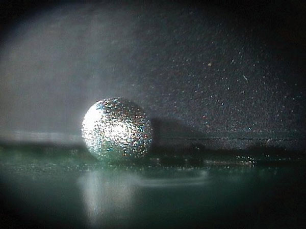
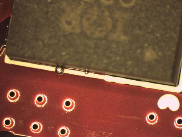
Figure 1. Examples of solder beads on BTCs.
FIGURE 2 is different, as solder has squeezed out of the component body during reflow. Lead-free solder has reflowed internally and been forced out of the package. It is most likely to have also migrated to other areas of the component and the circuit, creating other potential failure modes.
Figure 2. Solder reflowed internally, then squeezed out of BTC.
These are typical defects shown in the National Physical Laboratory’s interactive assembly and soldering defects database. The database (http://defectsdatabase.npl.co.uk), available to all this publication’s readers, allows engineers to search and view countless defects and solutions, or to submit defects online. To complement the defect of the month, NPL features the Defect Video of the Month, presented online by Bob Willis. This describes over 20 different failure modes, many with video examples of the defect occurring in real time.
is a consultant at the National Physical Laboratory (npl.co.uk); martin.wickham@npl.co.uk. His column appears monthly.


Press Releases
- Javad EMS Upgrades Through-Hole Soldering Capacity with New SEHO PowerWave System
- Sharpen Your Selective Soldering Skills with Kurtz Ersa's July VERSAFLOW 4/55 Training
- Omron Advances Inspection Technology with NVIDIA Omniverse and Metropolis
- Seika Machinery’s SMI 2026 Webinar Series Continues with Focus on PCB Cleaning Before Solder Paste Printing