Soldering With and Without Through Vias
 Imaged solder mask is preferred to filled vias to reduce voids and volatiles.
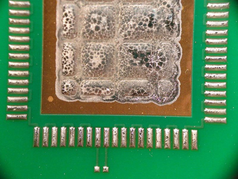
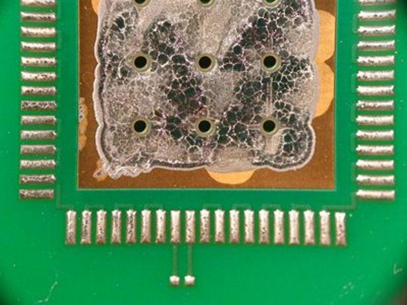
The QFN examples in FIGURE 1 compare soldering with and without through vias in the center pads. The difference is the correct paste stencil design and the use of solder mask around the vias. This prevents solder lost to the vias and has been shown to reduce void formation during reflow with convection and vapor phase soldering without the need for a vacuum.


Figure 1. QFN with through vias in center pads (left) and without vias (right).
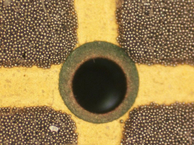
FIGURE 2 is a closeup of a through via with solder mask filling the via and solder paste printed with a segmented pattern, covering approximately 40 to 50% of the center pad. It is normally possible to reduce the volume further to reduce the amount of volatile material from the paste during reflow.

Figure 2. Solder mask-filled through via.
Ideally, it is preferred to have solder mask imaged and developed with rings around the vias, rather than filling the vias. Doing so increases the ability for any volatile to escape during soldering but still prevents solder from filling the vias. This technique has been shown to reduce void formation on many projects and is a simple, no-cost solution.
These are typical defects shown in the National Physical Laboratory’s interactive assembly and soldering defects database. The database (http://defectsdatabase.npl.co.uk), available to all this publication’s readers, allows engineers to search and view countless defects and solutions, or to submit defects online. To complement the defect of the month, NPL features the Defect Video of the Month, presented online by Bob Willis. This describes over 20 different failure modes, many with video examples of the defect occurring in real time.
is a consultant at the National Physical Laboratory (npl.co.uk); martin.wickham@npl.co.uk. His column appears monthly.


