

The Role of Heterogeneous Integration in the AI Hardware Ecosystem

Does Moore’s law apply to the new HI frontier?
The IEEE International Electron Devices Meeting (IEDM) held a night panel discussion on Dec. 10 titled Rest in Peace Moore’s Law, Long Live AI. As the title suggests, the discussion focused on the future of computing and the role of hardware. The moderator proposed questions like will CMOS technology become commoditized and differentiation occur mostly in circuit design, algorithm and architecture development? Will special purpose coprocessor adoption rates accelerate beyond CPUs and GPUs? What is the role of heterogeneous integration in the AI hardware ecosystem? Will the traditional memory hierarchy be upended by the arrival of non-volatile memory? Will analog accelerators using non-volatile memory elements drive the future semiconductor roadmap as scaling slows, enabling exponential improvements in compute efficiency and performance? Not all the questions were answered, but the discussion was lively.
The panel was moderated by Vijay Narayanan, IBM Research, with panel members from major OEMs, chip makers, packaging foundries and academia. The firstsection focused on the health of Moore’s Law.
Wilfried Haensch of IBM Research quoted an Apr. 19, 2015, article in The Economist that explained the end of Moore’s law. The article explained Gordon Moore’s economic observation in 1965 that by shrinking transistors, it would be possible to double the number of transistors that fit onto an integrated circuit every year (revised to roughly every two years), providing a cost advantage to scaling. Haensch indicated economics is critical in artificial intelligence (AI) and the deep learning explosion. Showing a slide from IDC on worldwide growth in the AI market, he projected that AI machine learning is the next IT. Is heterogeneous integration (HI) Moore’s law 2.0? According to Haensh, Moore’s law is based on economics (observation) and represents a tradeoff between productivity and yield. The tradeoff will continue, but the cadence will not. HI adds complexity to the component. AI solutions are, generally speaking, accelerators for specific tasks. Accelerators will provide better utilization and power/performance than simply using a CPU-based solution.
Mike Henry from Mythic, an AI accelerator startup, commented that cost improvements are on a flat line. Memory density, power, and bandwidth are concerns. Linear digital designs, no matter how integrated, won’t help shrinking modules. What will help, he said, is technology that solves power density and bandwidth of the memory. Putting the compute as close to the memory as possible is essential.
Dimitri Stukov, a professor from University of California, Santa Barbara discussed use of in-memory computing to prolong Moore’s law scaling. Ron Ho of Facebook also referred to Moore’s landmark paper, while noting the minimum cost point vs. yield loss, stating, “It’s all about economics.” Cost is an important, self-fulfilling prophecy. Ho discussed five data points, including the energy cost of monitoring data off-chip vs. on-chip. “Whether or not Moore’s law is dead does not matter,” Ho asserted. “What is important is yield for energy. Sustaining power solutions is the line now, not cost.”
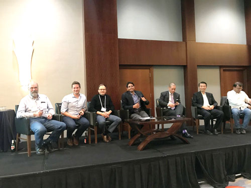 Figure 1. Members of the IEEE International Electron Devices Meeting IEDM panel.
Douglas Yu from TSMC indicated HI helps the Moore’s law concept for logic-to-logic integration and stated Moore’s law is alive and well, enhanced by HI! He commented on the new era in packaging for microprocessor, CPU, FPGA and AI accelerators based on options such as Intel’s embedded multi-die interconnect bridge (EMIB), and TSMC’s chip-on-wafer-on-substrate (CoWoS) and integrated fan-out on substrate (InFOoS) or InFO_MS (MS for memory stack), including transition to the use of high bandwidth memory (HBM) stacks and UMD. Yu discussed new 3-D interconnect options, such as TSMC’s system on integrated chips (SoIC) + CoWoS and SoIC + InFO. Yu calls this a new era in frontend plus backend (FE+BE), holistic 3-D HI, and indicated there are tremendous advantages to best optimize system power, performance, area and cost (PPAC) for “More Moore” and “More-than-Moore.” While Moore’s law 1.0 is about SoC scaling, 2-D scaling and transistor scaling, Moore’s law 2.0 is about system-on-package (SoP) scaling and 3-D interconnect density (3DID) scaling. TSMC is also proposing a new metric to show 3-D interconnect density: number of line and traces/mm across chip boundaries on an interposer, or substrate multiplied by the number of vertical interconnects (min. pitch) between stacked chips/mm2.
Vivek De of Intel argued Moore’s law and AI are better together, and no exponential is forever. It is not a one or the other discussion. AI today is because of Moore’s Law. HI, 2-D/3-D, processing big data, AI deep learning, logic, DRAM, and NAND all are Moore’s Law plays. Moore’s law may have stopped moving as fast in 1975 and slowed down, but this does not mean there is demise.
A second discussion topic focused on digital vs. analog, with a perspective on custom accelerators vs. CPU and the role of HI. IBM Research’s Haensch indicated hardware design takes advantage of AI algorithms. HI is needed to further decrease bandwidth constraints on data rate for memory access. Logic needs memory access without latency to function properly. Analog and digital will coexist and are best integrated. Analog has some advantages for custom accelerators. Stukov also indicated a focus on analog hardware is good for neuro inferencing. Ho of Facebook discussed the application of augmented reality glasses. Power is one of his critical concerns. A custom accelerator could help the latency problem.
The third topic looked in the crystal ball. IBM predicts one of the major drivers in human-machine interaction will be “i-shopping,” focused on targeted retail marketing, instant identification, and personalized advertising. Mystic discussed disruptions such as 5G and lack of understanding of the impact AI has on us. Intel discussed integrated ReRAM and logic technology beyond CMOS. Stukov described AI as a technology that will influence the future computer landscape.
Yu proposed the concept of immersion in memory compute for the future, where one would integrate multi-cores logic + memory with closest proximity logic-to-logic and logic-to-memory for AI. He also explained the concept of deep partitioning. InFO and CoWoS are backend 3-D solutions for heterogeneous integration. (They encompass DDR/GDDR and eDRAM, as well as HBM.) SoIC is frontend 3-D that enables deep partition, permitting logic that is not easily scaled to be partitioned. Deep partitioning focuses on scaling in the core for high-density and removing parts that can be pulled off but packaged together. Deep partitioning provides continuous improvement on total cost, time-to-market, performance, and power.
Intel’s future look included neuromorphic computing, distributed autonomous learning, and neural networks. De indicated that while there has been a slowing of the transistor in the past 50 years, power is the ultimate limit of Moore’s law. He indicated High K Metal Gate (HKMG) and FinFET developments are cost-effective developments. New switch devices can be expected as architecture innovates.
is president of TechSearch International (techsearchinc.com); jan@techsearchinc.com. Follow her on twitter @Jan_TechSearch.


Press Releases
- Altus Adds LPKF CuttingMaster 3290 to Depaneling Portfolio
- Kurtz Ersa Partners with E-tronix for Sales in Illinois and Wisconsin
- XLR8 EMS Welcomes Raul Jorge Lopez Jr. as Director of Program Management and Procurement
- Koh Young America Promotes Ramiro Mora to Lead Service and Applications in Mexico and South America