PCB Warping Causes and Prevention Strategies

Are your components in balance?
Warping of flat or planar printed circuit boards is a significant yet common problem when manufacturing and assembling PCBs.
Warpage can prevent pick-and-place machines from accurately placing components. Warpage can cause the lead-free wave solder machine to pick up solder and flood the board with solder. Even worse, a warped printed circuit may not fit in the case or cause problems with automated handling equipment (buffers, etc.).
A few items cause warpage, all known and preventable. The primary reason why a PCB will warp is uneven or imbalanced copper percentages in different layers. When a design is presented to a PCB manufacturer, the fabricator will run a check of the percentage of copper on each layer. This is to ensure the design is balanced; i.e., the copper plane percentages are even about the center. Consider, for instance, a typical 8-layer PCB. A copper power plane would be on layers 4 and 5 and signal layers on the remaining layers. The innerlayer 4-5 has an almost full copper percentage on both sides. The remaining layers are low-copper-percentage signal layers. The stresses locked in by lamination will even out or equilibrate.
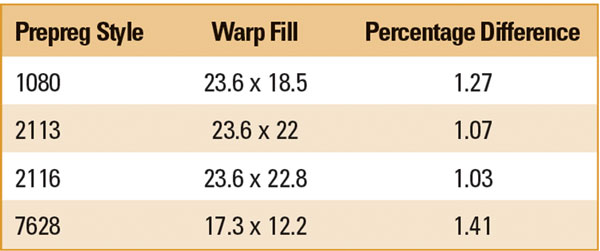
When raw laminate is manufactured, the resin, glass fibers and copper are all compressed, heated, and cooled at the same time. Sheets of laminate are very flat when purchased, but they also have “locked-in” stress. The top and bottom copper foil has a lot of strength to control the movement of glass fibers and resin; this is called modulus. When the sheet is laminated at high temperatures, the glass fibers and resin move around somewhat and in different amounts based on their coefficient of thermal expansion (CTE). Also, the woven glass fibers are not necessarily of the same density in the x and y directions, often called warp in the x direction, and weft or fill in the y. Glass prepregs such as 2113 and 2116 have almost even numbers of fibers in both directions, whereas prepreg such as 1080 and 7628 have a larger, different number of fibers in the two different weaves. This means they move more in one direction than the other, creating the potential for warpage (TABLE 1).
Table 1. Warpage Tendency for Common Prepregs

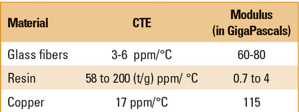
For the lowest warpage, select 2113 or 2116 as the prepreg. When the glass fibers and resin are laminated with the copper sheets, each part of the package will have a wildly different CTE and modulus! Examples are shown in TABLE 2.
Table 2. CTE and Modulus Variations

The copper exerts the stronger force of the three; the glass fibers are half as strong but only expand 1/3 the amount of the copper, so they are a controlling factor in the x-y axes only. The resin is the weakest as far as strength is concerned but expands three to 10 times as much. Copper is strong enough (modulus) to keep the glass fibers and epoxy in check. However, once etching removes a significant part of the copper, the locked stresses in the resin are released, which expands the PCB unevenly. The percentage of copper etched off will affect the amount each layer will expand, and thus cause warping of the PCB.
Processing a warped board is one of the biggest challenges in PCB assembly. A flat board that begins to warp will warp further as the heat of soldering releases pent-up stress inside the PCB. The single most significant reason for warpage is unequal thickness of copper layers not balanced relative to the center layer of the PCB. In multilayer boards, distributing copper area and weight equally around the theoretical centerline (middle) minimizes warpage.
The typical multilayer PCB is made of epoxy-glass laminate. The epoxy resin is subject to expansion and movement at temperatures above the glass transition temperature (Tg). This is acute during soldering operations, where the substrate is exposed to temperatures of 219° to 260°C. Various struggles are being fought inside the PCB as temperatures rise. The epoxy, which expands the most but with the least modulus (strength), will try to expand in all directions. The glass fibers and copper layers will use their lower CTE and higher modulus to restrict the epoxy expansion in the x-y directions. Therefore, the z-axis is relatively free to expand, which can result in some degree of warpage, sagging or bowing between corners.
The copper percentage ratio of an imbalanced PCB design after etching for each layer is shown in TABLE 3. The second row of percentages shows the improvement after copper pouring.
Table 3. Copper Percentage Ratio of an Imbalanced Design Post-Etching

In the typical example noted above, the original PCB design as supplied would have experienced more than 3% warpage. After the designer repaired the files using copper pour equalization, the distribution of copper among all dielectric layers becomes even about the center. The PCB will have 0.25% warpage, well within the 0.75% parameter in industry specifications.
The primary solution for minimizing PCB warpage is to use the correct copper weight and copper-etched percentage balance between dielectric layers and copper layers around the center in the PCB. For proper warpage control during the soldering and assembly process, use appropriate (and sufficient) clamp-down fixturing to hold the PCB flat during soldering. At the design stage, keep in mind component “balance” with regard to heat-producing components, i.e., how they are evenly distributed across the PCB assembly.
is chief executive officer of Rush PCB Inc., a printed circuit design, fabrication and assembly company (rushpcb.com); roy@rushpcb.com.
Press Releases
- Aven Welcomes Max Ramos to Strengthen Distribution Partner Operations
- ubersmt Expands SMT Line with Juki G-Titan Printer and RS-1R Placement System
- Keiron Technologies to Host LiFT Webinar Focusing on Solving Solder Paste Printing Challenges
- Express Manufacturing, Inc. Strengthens Test Capability with Acculogic Flying Probe System


