

Designing for Board Thickness
 Small differences can have big consequences.
For as long as there have been printed circuit boards, the nominal thickness seems to have been set at 0.062″ – or in Latin, 1.5748mm, but call it 1.6mm for short. In practical terms, the standard dielectric materials available support this board thickness while providing anything from two to 20 layers. I imagine four layers is still the most common use case.
Larger boards will need more connections and require more stiffness. To manage connectivity and flatness requirements, standard PCB thickness targets ratchet up to 2.4mm and 3.2mm. On the low side we find 1.0mm and go down to 0.8mm. All these targets are related to using so-called gold fingers as a printed edge connector.
It’s about connectivity and solderability. This was handed down from the backplane and daughtercard configurations found in our tower computer systems. The motherboard has expansion sockets and the memory cards come with fingers to plug and play. As a result of this variety, many connector vendors that market to plated through-hole technology users will offer different pin lengths that fit the range of board thickness options.
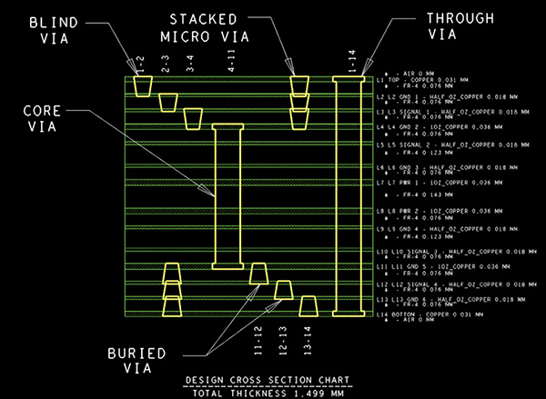
Figure 1. A 14-layer board where the stack-up would be designated as a 3-N-3 as a general case to describe the number of lamination sequences and a 3-8-3 for a more specific case to designate the total number of layers.
One edge connector vendor has an offering that accommodates boards between 1.37mm and 1.8mm. You have to imagine some flexibility is due when the PCB thickness variance is considered. This is probably this column’s most important takeaway. The construction of the board with all the material and process variables gives rise to a +/-10% process window in terms of PCB thickness.
Tolerance stacks up quickly. Doing the math for a standard 1.6mm board gives us 1.6mm minus 0.16mm, or 1.44mm on the thin side and up to 1.76mm on the high end. The broad thickness range for the connector mentioned above is just right for this application. The problem is not all the mechanical engineering world is fully aware of this limitation – not by a long shot. While thinner boards tighten up the process, thick ones need more than the standard allotment for the Z-axis.
Case study: Two possible thermal solutions; one winner. We had a QFN component that ran really hot and would fail. It had a good-sized ground paddle in the middle where the plugged vias were not up to the task. The mechanical designer decided to cut a slot in the board under the ground paddle. Then he would position the board over a pedestal that passed through the slot. He wanted a very thin layer of thermal grease on the top of the pedestal rather than a thermally conductive pad.
He also wanted a limit on the board thickness of +/-0.10mm rather than the +/-0.16mm I was calling out. I said he couldn’t have a tight tolerance on the stackup. The height of the pedestal was going to be predicated on hemming in the PCB fabrication process. You can do that with an aluminum billet but not with a cured strata of copper, glass and resin. We taped out a board with his specs and let the chips fall where they may. Of course, there was DfM pushback on the thickness callout.
We also did a parallel project in which I added DuPont CB100 thermal fill to all the ground paddle vias; not just the ones under the problem child but anywhere they would put a check on thermal issues. Finally, the day came when the two boards faced off and measurements were taken.
This was a case where the EE effort won out over the ME version by a good margin. The thermal vias were not affected by variations in PCB thickness. They were a bit of a cost concern, but the project moved forward with the thermal problem solved. The moral of that story is that we can’t put tight controls on multilayer PCBs. If you want to be in the game, you must be the bearer of this cold, hard fact.
Is it “in to be thin?” There is a lot to be said for thinner boards. They have a singular attribute where they can be depaneled with lasers rather than traditional milling or V-score. As far as I know, the maximum thickness for the laser treatment is 0.5mm. Makers of laser ablating machines don’t brag about their maximum cutting depth.
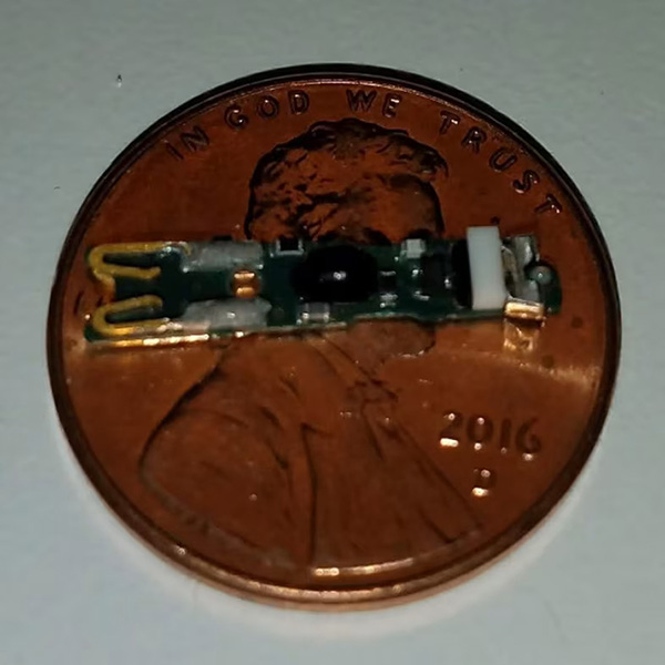
Figure 2. This must be the smallest PCB I’ve ever met. Let’s just say that some rules were bent in the making of this board.
What I learned about it is from working with a specialty PCB vendor that focused on optical solutions. It seems to be about the number of passes to cut through the dielectric materials and any metal that may be present. One of the bugs encountered in laser depanelization is when the laser scorches the board edge. It’s called carbonization (along with some other not-so-nice words).
One nice thing you can do for these thinner boards is provide sufficient mounting hardware locations so that board flexing does not stress the solder joints. In this case, three generous slots provide mounting locations for these quirky printed circuit boards.
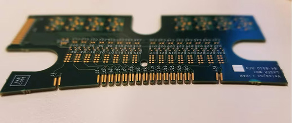
Figure 3. Laser depanelization is a must to get this intricate shape.
What we gained other than a fancy outline was the ability to handle finer edge-to-copper minimums. That may sound like a small win, until you consider the orthogonal board-to-board fusion we had going on there. Groovy little cutouts accept ridiculous little boards that shoot lasers everywhere while an equal number of detectors spin in harmony to catch the rebounding light off the local terrain. These lidar sensors put the fabricators to the test. All my round boards came from this platform.
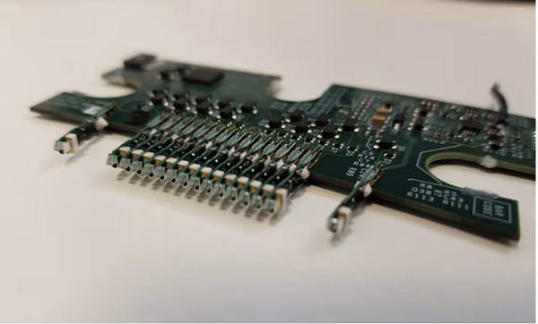
Figure 4. The tiny boards meet the little board in an unusual connector-less fashion. Giving sensory perception to a machine can require some out of the box thinking.
To wind this up, there are tradeoffs to consider for each PCB project. Working out the routing scheme through fan-out studies and experience gets you to the optimum layer count. The electrical and mechanical constraints add the spice to the mix where the z-axis gaps between metal layers are established. Simple things like metal loading have a direct effect on the geometry. Having some traces on a layer is not the same as a copper pour in terms of the outcome.
Those factors add up to the total board thickness. Solder mask and other treatments add small but potentially significant differences. A board could swell just from a humid environment. That’s why assemblers routinely prebake boards prior to assembly. No surprise that there are a lot of variables when it comes to PCB thickness.
is a career PCB designer experienced in military, telecom, consumer hardware and, lately, the automotive industry. Originally, he was an RF specialist but is compelled to flip the bit now and then to fill the need for high-speed digital design. He enjoys playing bass and racing bikes when he’s not writing about or performing PCB layout. His column is produced by Cadence Design Systems and runs monthly.


