

Metal Health: Know Your Copper Thicknesses
 Whether in wire or trace form, keep copper thickness in mind for your design.
Once upon a time, about eight decades back, we didn’t have printed circuit boards. We had copper wires that came in various diameters. Carrying a larger amount of current requires conductors of a larger diameter. These various diameters were identified by the American Wire Gauge (AWG) where smaller numbers indicated thicker wires. There is a metric equivalent where the opposite is true – a higher number for a thicker conductor. Set that aside for this discussion.
Heavy gauge wire for power. A 12- to 14-gauge wire is about the diameter of a cooked spaghetti noodle (~2mm) and is commonly found in power cords for smaller electronics such as a table lamp or a fan. An electric dryer running on 220V will require something between 10- and 6-gauge wire depending on the amperage of the appliance. Again, smaller numbers refer to larger cross-sections.
For the sake of flexibility, these thicker wires are typically constructed of several smaller wires twisted like a candy cane prior to adding the insulation coating. The coating itself is not part of the gauge, only the conductor matters in that regard.
Connection wire for signals. Then you have a 30-gauge wire, which is more like angel hair pasta. The diameter is 0.25mm, yielding a cross-section of roughly 0.05mm. This will be a single strand of wire and is typical of the “white wire” used to rework/repair a printed circuit board. The maximum current rating for 30-gauge wire is 500mA, which is fine for the intended signals.
General purpose wire. Between the 12 and 30 AWG conductors is 18-gauge, which can be used for general connections such as speaker wire. At 1mm of diameter, this gauge is rated at 7A when using polyvinyl chloride (PVC) for insulation. Teflon-coated wire has a higher operating temperature, so the same wire bundle can handle a bit more current without going up in smoke. This is analogous to using high-performance dielectrics on a printed circuit board.
As a factory worker in the mid to late ’80s, I was soldering 12-, 18- and 30-gauge wires to assemble telecom racks. Those 7ˈ to 11ˈ tall units permitted a single T1 phone line to carry from 384 up to 528 separate signals through digitization. This was much better than the 24 analog signals (12 actual conversations) that the T1 line originally supported. The antitrust breakup of AT&T meant that all of the Baby Bells had to pay up to get the enabling equipment. So-called rack wire and test was my entry into high tech – 40 years ago!
Coaxial wire: One step beyond a twisted pair. Credited to Oliver Heavyside in an 1880 patent, a special type of wire known as coax features a non-stranded conductor inside an insulator that is then wrapped by a weave of copper with another layer of insulation around the weave. The woven shield is used as the ground path for the transmission line.
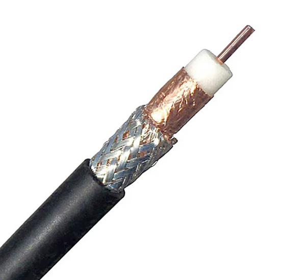
Figure 1. A coaxial cable creates a Faraday cage around the central conductor. The isolation and controlled impedance permit much longer runs without signal degradation. (Source: BHPhotoVideo)
This wire within a wire provides a controlled impedance environment of 75Ω for the central strand, with the weave also acting to mitigate electromagnetic interference between the inner wire and any outside sources. The coaxial arrangement protects the outside world from the noise inside the cable as well as isolating the inside from the environmental effects beyond.
Wire compared to PCB traces. All the ratings for hook-up wire have a corresponding cross-section to the traces on a PCB. The primary difference is the wire is round while the traces are more of a trapezoid that tapers toward the top. The average thickness and width of the trace determine the current capacity, while the type of dielectric material governs how much temperature rise is acceptable. The advantage of wires is in the connection flexibility, where the traces shine in terms of handling more complex circuits in less space.
Copper thickness is measured by weight. One of the oddities related to plating has to do with the way the thickness of copper is specified. You may have heard of 1 oz. copper or some other number like that. The unit of measure is based on 1 sq. ft. of copper. Whatever that square foot weighed would be the value of that thickness.
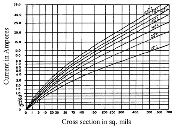
Figure 2. Before tools or apps could solve metallization requirements, these current carrying capacity charts were used to determine conductor width. This chart shows how much of cross-section is required for a given temperature rise. The lower, more conservative numbers of 30° of rise or less are preferred. A current of 5A with an expected temperature rise of 20°C require a cross-section of 100 mils. (Source: IPC)
Starting plating vs. finished plating. Fabrication drawings refer to finished copper thickness. The reason for this is that 1 oz. copper is only the beginning. A full PCB panel with copper on both sides is drilled for all the plated through-holes in the design prior to any etch process. In simple two-layer terms, this is all one core. For a four-layer stackup, innerlayers have been etched with a circuit pattern prior to lamination.
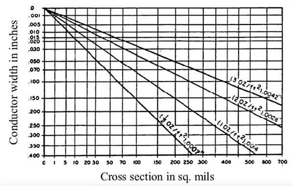
Figure 3. Sticking with the 5A current estimate and 20°C allowable temperature rise, the 100-square-mil target is found using 1 oz. copper that is about 75 mils (1.9mm) wide. Using 0.5 oz. copper would require double the width for the same outcome. (Source: IPC)
Now you have a board where the outer layers are still solid copper. This is the point when the drilling operation takes place. The whole board is still shorted out at this stage. The board is seeded with an electroless copper deposition process that lays down a very thin layer of copper inside the holes. After that, electrodes are attached to the outer plating layers and the whole thing is run through various processes that add more copper and finally some tin to the “barrel” of the holes. For this reason, the copper in the barrel will always be thinner than the copper on the outer layers that have the advantage of starting out with the original plating.
Considerations for high-density interconnect. High-density interconnect (HDI) uses a sequential lamination process where each layer that has microvias will also have plate up beyond the original copper. Much like the four-layer board in the above example, the layers that do not get plated up are in-between the first and last layers of any core vias that may be present. For example, the 14-layer stack-up in Figure 2 with a core via from layer 3 to layer 11 would plate up all layers except those between layer 4 and layer 10.
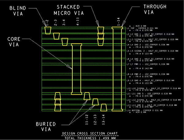
Figure 4. A diagram labeling the classes of vias in a typical HDI stackup. Plating-up via connections is one of the considerations for overall board thickness as the process adds material to the metal layers. (Source: Author)
Ultra-high density (MSAP). The significance of not plating up is that the layers that didn’t terminate a normal blind or buried via (L4-L10) would be the only layers where modified semi-additive process (MSAP) could be used. The starting copper for MSAP is only a fraction of the usual copper thickness. A mask is put over the areas to be removed and the rest is plated up. This creates high and low areas. The high areas are retained by another mask where we want a circuit pattern, and the low areas are subsequently microetched away to reveal the circuit pattern. The initial plating has a lot in common with the first step of chemically plating the vias. They use a very thin layer of copper and electroplate up to the required finished thickness.
Metal core PCB. Let’s finish up with one of my favorite examples. Known as “The Stick,” it’s for a CDMA (3G) multi-carrier RF amplifier to be used inside the little hut at the bottom of every cellular tower. The first time I was listed as a contributor on a patent was for the innovative via structure with a “backdrill” that started from the top. Notice Figure 5 where you can see the black dots along the edges of the device cavities. They are effectively used as ground vias from layers 2-4. The leads of the amplifier chips solder right over the top of the drilled and filled counterbores.
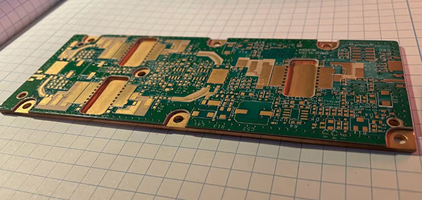
Figure 5. A metal core board that uses 32 oz. copper for layer 4. The copper pallet makes up about 75% of the board’s overall thickness. (Source: Author)
This is only four layers, but the solid copper bottom could have had another three layers below the copper slug for a total of seven. It’s surprisingly heavy for its size. The stiffness and flatness are better than average with this much copper. This isn’t very common, noting that the IPC charts only go as far as 3 oz. copper.
There is no circuit pattern at this metal thickness, but you can see where the board is relieved to expose the mounting holes. Meanwhile, the device cavities go deeper with cutouts that hog out some of the copper slug. That is done to permit the device pins to align with the top surface. This is a board with two outlines and three thicknesses. Layer 4 is rectangular with the other layers having cut-outs and slots. This is a different way of thinking beyond heavy copper.
The funny thing is that you can still find these 13cm, 75W amplifiers being sold online decades after the company, Spectrian, went under. This may be the most reliable piece of equipment I’ve designed – provided you get the ones with the Motorola chips rather than our homespun LDMOS devices.
is a career PCB designer experienced in military, telecom, consumer hardware and, lately, the automotive industry. Originally, he was an RF specialist but is compelled to flip the bit now and then to fill the need for high-speed digital design. He enjoys playing bass and racing bikes when he’s not writing about or performing PCB layout. His column is produced by Cadence Design Systems and runs monthly.


Press Releases
- Javad EMS Upgrades Through-Hole Soldering Capacity with New SEHO PowerWave System
- Sharpen Your Selective Soldering Skills with Kurtz Ersa's July VERSAFLOW 4/55 Training
- Omron Advances Inspection Technology with NVIDIA Omniverse and Metropolis
- Seika Machinery’s SMI 2026 Webinar Series Continues with Focus on PCB Cleaning Before Solder Paste Printing