An experiment investigating print alignment adjustments.
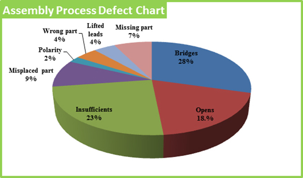
Printed circuit board assembly requires extraordinary precision and repeatability. The screen printing process is considered the most critical process in the surface mount technology (SMT) assembly process. According to some studies, 70% of SMT defects can be traced back to the screen printing process (FIGURE 1). Component miniaturization has made this process more critical. Therefore, alignment of the apertures in the screen or stencil is key to an efficient and accurate solder paste transfer and there isn’t such a thing as local offset.

Figure 1. Solder paste defects, per Koh Young.
Claire Wemp is hot on the trail of better thermal interface materials and more engineering roles for women.
Thermal interface materials (TIM) are used between components to help with heat dissipation. Claire Wemp, Ph.D., is a thermal applications engineer at DuPont, with a doctorate in mechanical engineering, where her research was on heat transfer enhancement for metal surfaces. While an undergraduate, Wemp also became involved in the Society of Women Engineers, and continues to work with the nonprofit professional organization today. Wemp joined PCD&F/CIRCUITS ASSEMBLY on the PCB Chat podcast, where she discussed the use of TIMs and her work with SWE. What follows is a lightly edited transcript.
The unstructured evolution of integrated circuit package technology (and its consequences).
I purchased my first "integrated circuit" around 1957, which was roughly a year before Jack Kilby is credited with inventing the IC. In appearance, it was a paper phenolic PCB with six discrete transistors in TO-cans and a few axial-leaded resistors and capacitors soldered on one side. If one can stretch their thinking just a bit, however, one can see the truth of the suggestion that it was arguably an "integrated circuit." The fact that Kilby was working at Centralab in Milwaukee, a ceramic circuit maker, immediately before heading to Texas Instruments for his new job was fortuitous. I have long assumed it influenced his invention. Around the same time, the IC's recognized co-inventor, Robert Noyce, took the idea a step further and showed how transistors and interconnections could be built on silicon wafer, which remains the primary method used today – featuring sizes a few orders of magnitude smaller and significantly increased material sets to embrace many new semiconductor materials in addition to silicon.
The PCBAA is ramping up efforts to secure funding for R&D and capacity in the US.
What constitutes the printed circuit board industry? And how much, if any, investment should the US government allocate toward ensuring its technological and capacity capabilities?
These are among the questions David Schild is tackling every day. Schild is executive director of the Printed Circuit Board Association of America, which was founded in 2021 to advance US domestic production of PCBs and base materials. The organization is made up of corporate members of all sizes and includes fabricators, assemblers and suppliers.
Schild addressed questions about public and private investment, how governments can help create "demand signals," and the PCBAA's annual meeting with PCEA for the PCB Chat podcast in late July. The following transcript has been lightly edited for clarity and length.
Can predicting board and part flatness at critical points in the reflow/reliability profile reduce failures?
Surface warpage, or flatness, is an established source of reliability issues in surface mount devices (SMD), particularly when these surfaces are considered as they warp due to heat generated in production or real-world use.1-6 Thermal warpage of surface mount components such as ball grid arrays (BGA) and line grid arrays (LGA) are subject to different industry standards from JEDEC, JEITA, and IPC, based on sample size, ball size and ball pitch.7-9 Further SMD studies have proposed different methods of classifying and qualifying surface shape in hopes to improve the correlation in thermal warpage data and product reliability.10 Meanwhile, printed circuit boards are less regulated for warpage in the area where an SMD may attach. Overall PCB warpage is referenced in some industry standards and technical papers, but specific warpage limits are lacking within documentation discussing warpage of SMD landing areas.11-12 Finally, further studies have considered warpage of both SMD and PCB landing areas together.13-14
Match the resources that make sense in the scale of your operation.
In the early 1990s, some observers were predicting that the EMS market would consolidate and shrink to a handful of large players building the bulk of the world’s electronics products. But outsourced electronics manufacturing isn’t a one-size-fits-all equation. Even large OEMs often have higher mix, lower volume or variable demand segments of business that fit best in a regional EMS provider. Consequently, regional EMS providers continue to thrive.
Press Releases
- Koh Young Announces Two Sales and Service Changes to Strengthen its Customers in the US and Canada
- Express Manufacturing, Inc. (EMI) Promotes David Vue to Lead Military and Aerospace Division
- SP Manufacturing Expands into UK Avionics Sector, Secures First Customer Engagement
- Kodiak Assembly Solutions Strengthen Domestic PCB Supply Chain Amid AI-Driven Market Pressures


