


Custom nozzles can reduce processing time and improve selective soldering machine flexibility.
Somewhere between the polar opposites of point-to-point selective soldering and mass solder dipping lies a unique happy medium known as stamp soldering. Stamp soldering in fact is a rather broad term, but what I’m talking about here is something of a middle ground between the two: an offbeat type of stamp soldering that can be achieved with a conventional selective soldering machine and that saves a tremendous amount of processing time while actually extending or expanding the flexibility of the conventional selective soldering machine.
The basics of conventional selective soldering are known to most. A single nozzle mounted on a solder pot and fountain travels around the underside of a PCB, soldering specific sites according to an individual sequential program created for that board. This method is very flexible and permits rapid changeover between products. However, the time it takes (TAKT) to process that board in its entirety, and each successive one, is a direct function of the number of solder sites on that board and the dimensions of the board itself. For example, a single board, as large as 18" square with 500 solder points might take as long as 5 to 7 min. to process, since each point must be soldered individually.
At the opposite end of the spectrum is the mass solder-dipping technology (conventional wave), which isn’t actually dipping at all but involves the use of custom fixtures and various forms of masking over a solder fountain source; the fixture has apertures to match the solder points on the PCB, which again could be as large as 18" square. All the solder sites on that board are replicated in a large solder wave. Expensive robotics position the board and fixture over the fountain/wave for a preset dwell time, after fluxing and preheating, and the PCB is soldered all at once. This latter method is suitable for very high-volume soldering and speed, for a fast TAKT time; that 18" square PCB might take only 10 sec. to process versus 5 to 7 min. the conventional way. However, the setup is dedicated to just one product and is quite difficult to change to a different product. The equipment is costly, as are the individual custom soldering fixtures. This method is also known as stamp soldering, but it is different from the “middle ground” that we discuss here.
Our middle ground stamp soldering can be accomplished using a conventional selective soldering machine fitted with a special stamp soldering nozzle. Granted, it’s a much smaller fixture than the one needed to mass solder a large board; in fact, the one shown in Figure 1 has only four apertures or nozzles mounted on it. It is a custom fixture designed for a specific board. The rectangular or longitudinal aperture is for a connector; the larger round aperture is for a round cluster of pins, and the two miniature twin nozzles are for soldering adjacent LED components. In a panelized PCB scenario, the custom nozzle indexes around from board to board and stamp solders that small pattern on each PCB. The nozzle can also be removed and exchanged simply with a standard nozzle for ordinary selective soldering routines.
The advantage of this nozzle is that it processes every board in the panel in exactly the same fashion vs. the mass technique that strikes all solder joints at once. So, the “selective stamp nozzle” is somewhere between the mass solder dip machine, which is very expensive and highly dedicated, and a conventional selective soldering machine, which is flexible and non-dedicated. This is actually a hybrid, with the only dedicated part being a small custom multi-port nozzle. When aperture sizes vary, to maintain uniformity of pressure and flow in all the apertures, threaded set screws are installed for each aperture so that the flow can be restricted or constricted in order to achieve balance.
In process, a dropjet fluxer applies flux only where it is needed, and if necessary, the board is preheated. The board is positioned, checked with fiducials to make sure it’s in place, and then the solder pot, with its pumped aperture, comes up and contacts all the solder sites at once, effectively making the solder joints, and then drops out of the way under programmed control.
This pattern could, of course, be sequentially soldered using a single nozzle, with the time needed to solder the entire pattern estimated at about 40 sec. Using the custom stamping fixture in a step and repeat sequence, all points might be soldered in 6 to 7 sec. If several hundred identical boards are to be soldered, the cumulative time savings become readily apparent. Perhaps the most significant aspect of this higher throughput rate is that it can be achieved using a run-of-the-mill, affordable selective soldering machine without any costly adaptation.
Alan Cable is president of A.C.E. Production Technologies (ace-protech.com); acable@ace-protech.com.
Relying on noncontact measures is preferable when looking for open BGA connections.
It is unfortunate, but mechanical testing of joints does happen on production boards. Figure 1 shows the result. The ball has broken off the BGA package and the PCB pad.

Mechanically probing BGA joints is poor practice, given the ready availability of inspection techniques like x-ray and endoscopes. We can all appreciate that, in some cases, inspection methods may have difficulty finding open connections, but great care needs to be taken if testing of suspect joints is to be considered.
It is clear from the damage to the ball surface and the joint interface that the termination has been subjected to a high force. It is very easy to apply well over 1kg of force with a toothpick, and this type of action should be avoided or well-documented.
These are typical defects shown in the National Physical Laboratory’s interactive assembly and soldering defects database. The database (http://defectsdatabase.npl.co.uk), available to all this publication’s readers, allows engineers to search and view countless defects and solutions, or to submit defects online. To complement the defect of the month, NPL features the “Defect Video of the Month,” presented online by Bob Willis. This describes over 20 different failure modes, many with video examples of the defect occurring in real time.
Chris Hunt is with the National Physical Laboratory Industry and Innovation division (npl.co.uk); chris.hunt@npl.co.uk. His column appears monthly.
A look back at friends and colleagues who left us in 2012.
A pair of true industry giants died in this past year, both pioneers in their own right. Olin King founded Space Craft Inc., which under its more common name SCI Systems (and later, Sanmina-SCI), is generally recognized as the first contract electronics assembler and, for a time, was also the largest EMS company in the world. For his part, Gene Marsh was an electronics design automation pioneer, bolting Raytheon for a career developing PCB software for the masses. The Gene Marsh Award for Technical Innovation is named for him.
Two other major league inventors also passed this year. All couch potatoes owe a nap of gratitude to Eugene Polley, who over his 47 years at Zenith rose from stock boy to become assistant division chief of Mechanical Engineering and counted the first wireless remote control among his 18 US patents. And anyone who sees the promise of green energy can appreciate Stanford Ovshinsky, who was assigned more than 400 patents, the most significant of which – the NiMH battery – is used in everything from laptop PCs to cellphones to electric cars, and who later developed flat screen LCDs and thin-film solar cells. This month we reflect on their impact on our industry and our lives.
(Harold) Gene Marsh, 84, launched PADS Software in 1975, one of four companies he founded.

Olin King, 78, founder Space Craft Inc. (later, SCI Systems); credited with founding the modern contract electronics assembly industry.
Robert (Bob) Bukowsky, 71, former IDEAL vice president of sales.
James Lee, 51, founder of PCB fabricator UniGlobal.
Mr. Xie, age unkown, Foxconn employee.
Steve Appleton, 51, CEO of Micron Technologies. 
Jackki Morris-Joyner, longtime IMAPS technical program manager. 
Stanford R. Ovshinsky, 89, semiconductor expert who invented the nickel-metal hydride battery and codeveloped solar energy panels and flat-panel displays.
Robert (Bob) Parker, 53, computer engineer at Universal Time Co.
David B. Speer, 61, ITW chairman and CEO.
Chris Lewis, 64, president, CEO, and co-founder of Dynawave Inc.
Hans Camenzind, 78, analog guru who introduced the phase-locked loop to IC design.
Mr. Yang, 22, Foxconn Shenzhen.
Eugene Polley, 96, longtime Zenith Electronics engineer and inventor of the wireless television remote control.
And one in late December 2011:
Gene Hendrickson, 79, former Tektronix engineer, president of General Management Integration (GMI), and founder of the October Project.
As the first distributor DNA-marked components are shipped, a look at how parts are “tagged” and traced.
SMT Corporation, an independent stocking distributor of electronic components, has begun shipping components marked with a DNA (deoxyribonucleic acid) taggant. The taggant was developed by and is supplied by Applied DNA Sciences (APDN) of Stony Brook, NY. The purpose of the marking program is to give the component user unalterable and traceable access to the part’s history and origin when marked and shipped by the original component manufacturer. In the case of open-market parts sourced by SMT, they will only be marked after they pass through its counterfeit mitigation and component quality inspection process.
The application of SMT’s DNA mark on a specific passing lot of components will effectively draw a line in the sand of provenance composed of detailed quality and authentication inspection documentation easily traceable back to an accessible copy of the SMT inspection report, a document that is valid for the life of the part. This DLA mandate to mark FSC 5962 microelectronics was announced in August, and would be required as of November.1
Depending on who marked the part, the taggant will provide to the user the downstream pedigree or provenance of the part throughout the entire subsequent path of the part. Carefully controlled during its evolving infancy within the electronics industry, the taggant will create what Tom Sharpe, vice president of SMT, believes to be the beginning of “our reliable wall of prevention” against counterfeiters.
“The severity of the counterfeit problem demands all parts that can be procured from the original component manufacturer, its authorized distributors or authorized after-market distributors, must come from those secure supply chains whenever possible,” Sharpe points out.
“It is only after those options have been thoroughly exhausted that a contractual procurement from a well-vetted open-market supplier should be considered.”
Until now, the absence of such proof has permitted the easy penetration of supply networks by counterfeit electronic components. It has also led to discoveries of counterfeit components installed in numerous sensitive defense and aerospace applications. And it has permitted the existence and continued operation of component distributors that seek big profits by buying components from highly suspect sources and reselling those components as authentic.
The DNA taggant will be carefully and permanently applied onto the surface of the components in SMT’s laboratories in Sandy Hook, CT. SMT buys components from respected authorized sources wherever possible – sources where authenticity can be safely assumed in most cases. When parts are obsolete and unavailable from trusted aftermarket manufacturers, it then becomes necessary to turn to the open market. In those cases, SMT conducts an exhaustive forensic component inspection to determine that the components are not counterfeit, and only then will provide them to defense and aerospace manufacturers, as well as all other high-reliability industry OEMs.
The intensive documented screening processes performed by SMT, together with the objective-evidence documentation provided with parts shipped, have made them the vendor of choice by many when it comes to procuring legacy components from the open market. Legacy components are those components no longer in production but vital to maintaining the readiness of military systems over time periods that may run to 20 years or more. SMT’s contract makes it clear to its suppliers in the open market that components found to be counterfeit will not be not paid for and will not be returned to the source.
The company has also devoted years to acquiring the tools and the sophisticated, detailed expertise to identify even the most clever counterfeits. A decade or more ago, counterfeits could often be identified by misspelled markings or crude imitations of logos. Today the tipoff to SMT may be the way the surface texture appears in a scanning electron microscope (SEM) at 5000x magnification, or the careful comparison of elemental analysis data gathered with x-ray fluorescence or energy-dispersive x-ray against the OCM’s materials composition data sheet.
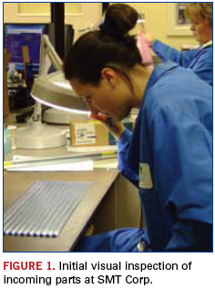
SMT uses multiple technologies beyond visual inspection and optical microscopy, such as SEM, EDX, scanning acoustic microscopy, digital microscopy, real-time x-ray imaging, XRF, cross-sectioning, de-lidding and die matching, solvent testing, electrical test, solderability testing and several others to evaluate large and small lots of diverse components (Figure 1). Some of these components are of course counterfeit. SMT’s technicians thus have a constant supply of components of unknown provenance, from which experience and databases can aid in spotting the many tiny anomalies that expose counterfeits.
In 2009, for example, they discovered a new coating virtually identical to the epoxy used in plastic-packaged components and immune to acetone surface-test swabbing used in the refurbishing of scrap components to sell them as new. The original component surface and markings were sanded off and new coating and markings applied. The initial tipoff was that the “superbug” coating was not applied perfectly on all parts. By the time the counterfeiters had improved the coating application process and were shipping lots of more consistently coated parts in 2010, SMT was working with a heated solvent (thanks to Honeywell Aerospace) that would dissolve the superbug coating without dissolving the epoxy.
A year later SMT identified and mitigated a new micro-blast technique being used by counterfeiters to remove the part markings from components without requiring a coating be applied to cover their handiwork. Later that same year, SMT identified and mitigated a lapping process being used to cosmetically renew the surfaces of ceramic and some metal component packages.
APDN developed and manufactures the taggants in the new program, which is known as SigNature DNA. The taggant has been described as a botanical DNA molecule that has been scrambled.2 One may think of the millions or hundreds of millions of bases in a DNA molecule, and the vast number of ways in which they could be rearranged, but the actual process is even more complex and non-reproducible. We are accustomed to think of DNA as fragile, and in its normal state, it is fragile. But APDN’s DNA has been processed to make it vastly more robust; it survives with its identifying structure intact.
SMT is the first distributor to ship DNA-marked components. The first shipments were preceded by a two-phase 18-month DLA project managed by the LMI consultancy, with supply chain participants, including SMT. The purpose of the two-part pilot program was 1) to demonstrate that components marked with SigNature DNA could move through supply channels, and 2) to work out the shipping, handling and pricing details of distribution throughout DLA’s microcircuit supply chain.
Toward the end of the pilot program, the DLA on Aug. 7, 2012, issued a mandate requiring that all FSC 5962 microcircuits supplied to the DLA be marked by SigNature DNA.1 Specifically, a new clause in solicitations and contracts “requires contractors to provide items that have been marked with botanically-generated DNA produced by Applied DNA Sciences or its authorized licensees, if any.”1 Less than a month later, APDN and SMT announced the first-ever contract agreement to begin shipping components with DNA provided by APDN.
The DNA technology has already been used to mark a range of products, including cash being moved to and from banks in the United Kingdom to wool suits made in the north of England. In an early phase of the collaboration, components made by Altera were DNA-marked. Some were then shipped to a distributor, while others were retained at Altera. Included in the lots of parts were some with no DNA taggant. Swabbing a total of 44 parts at both locations correctly identified those parts that were the specified Altera products and those that were unmarked (and therefore not traceable).3
During the pilot program, the DLA engaged an independent laboratory to attempt to defeat the DNA technology – in other words, to find some means by which counterfeiters could circumvent the technology. No such means could be found.
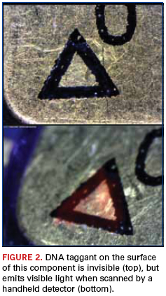
The taggant as applied on components shipped by SMT will be covert, i.e., invisible. The recipient of a lot of marked components scans them with a handheld detector, which will cause the taggant, even if covert, to emit visible light (Figure 2). The laser does not “read” the taggant; it simply affirms that a taggant has been applied.
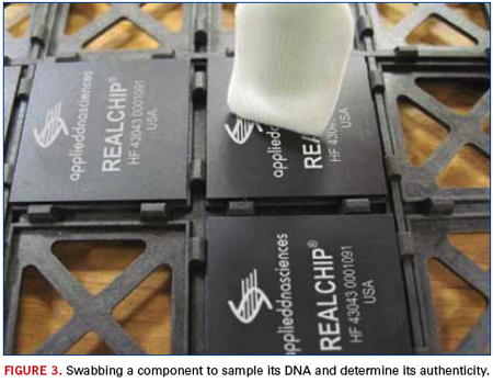
For specific and fully forensic verification, the recipient swabs one or more components in a shipment (Figure 3) and sends the swabs to APDN. In 72 hr. or less they will learn whether the taggant matches perfectly the APDN taggant that was applied by Manufacturer/Supplier X onto Part Y. Applied DNA states that the mark is flatly not copyable. Counterfeiters hoping to create a credible counterfeit part will find that duplicating APDN’s taggant is a fantastic impossibility.
The DNA taggant can be embedded in the ink already used to mark many types of components. If the manufacturer uses ink, there will be no change to line processes, simply a switch to the taggant ink, which is being supplied by Markem Imaje. If a component is currently marked only by a laser-etched label, a visible or covert ink dot can be added. The surface to be marked by the taggant can be plastic, metal or ceramic, can be very small, and does not need to be flat. For security purposes, a company’s unique DNA formulation will be changed every 12 months, although it may be changed at a shorter interval if desired.
In the short-term, DNA-marked components will become a powerful tool in weeding out counterfeits from components flowing into defense and aerospace use. The personnel who depend on their equipment to perform as required will have enhanced reassurance that it contains no fraudulent electronic components.
References
1. Defense Logistics Agency, DLA Internet Bid Board System, DNA Authentication Marking on Items in FSC 5962, Aug. 7, 2012.
2. Mike Buetow, “Cell Block,” CIRCUITS ASSEMBLY, February 2011.
3. Beth Reece, “DLA, Industry Fight Counterfeits with DNA Technology,” Defense Logistics Agency press release, Jan. 23, 2012.
Tom Adams is a consultant to SMT Corp. (smtcorp.com).
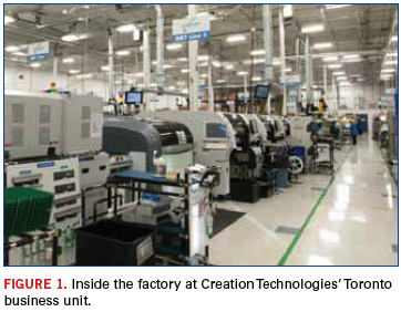
Creation Technologies is building a stellar contract assembly model, one acquisition at a time.
Over the course of my 20 years in the industry, I’ve visited well over a hundred electronics assembly plants, and when it comes to today’s SMT operations, the variances are usually subtle – if they exist at all.
Sure, there are almost as many financial models as there are EMS companies, but once we move from the back offices to the factory floor, commonality prevails. A few companies may break the mold, but they are so few and far between, you just stop expecting to be surprised.
Creation Technologies was a surprise, and in more ways than one.
A privately held company, Creation prides itself on being one of the best-kept secrets in EMS today. Shielding itself as it does, however, obscures a long history of performance excellence, and a track record of growth to which few others can compare.
Most mid- and large-tier EMS companies have grown at least in part through acquisition. Creation is no exception, having snapped up, by our count, nine companies in its 21-year history. What’s remarkable is that Creation has never closed a site due to a lack of business. Ever. (They have outgrown a few.) For a large Western-based EMS of its size, that’s unheard of, and speaks well to its due diligence, management and execution.
Moreover, in an era of chasing low-wage manufacturing, 11 of Creation’s 13 factories are in the US or Canada. The company “gets by” with a single site in China and its just-acquired factory in Mexicali, Mexico, the former Aisling Industries.
Two for One
Another oddity: It’s not unusual for Creation to have multiple sites within earshot of each other. There are two in the Silicon Valley (Santa Clara and Milpitas), two in Burnaby, British Columbia (where Creation got its start in 1991 and is headquartered today), and two in Toronto (Mississauga, Markhem). Moreover, the suburban Milwaukee and suburban Chicago sites are just 60 miles apart. This model of overlap is by design. After a certain point, it would rather add a plant than endlessly expand an existing building. The company prefers facilities of 60,000 to 80,000 sq. ft., with a peak of roughly 350 workers and $75 million to $100 million in revenue. To wit, this year it expanded its site in China and added a 79,085 sq. ft. building in Milpitas after outgrowing its plant in nearby Santa Clara. (The exception would be facilities in low-cost regions, which can be larger.) Business units average three SMT lines, with a range of two to five.
The relative cozy nature of the sites helps keep operations manageable, explains Andy Hyatt, executive vice president – business development & regional leader East and Design Services. Once the Business Unit reaches about 350 workers, it’s time to look to split into a second unit for reasons both cultural and financial. At that point, he says, “We can’t have a town hall meeting with everyone in the same room. We don’t know everyone’s name. Once you reach a certain point, the more difficult it can be for the Leadership Team to pay attention to every customer.”
Creation relies on certain performance metrics to incentivize its employees to remain focused and engaged. Each business unit receives annual performance metrics against which they are monitored and measured. Staff also executes “engagement surveys” in which they are asked to reflect on how Creation is performing toward living its core values, making employees secure, and so on. The results of the surveys are one of six metrics that make up the company’s performance plan. A special sheet hangs where employees can call attention to one another for stellar work. One payoff is consistency; the employee retention rate is 94%.
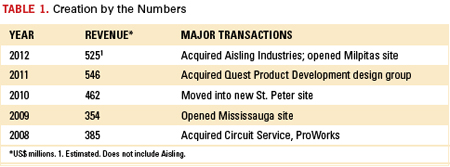
Through acquisition and execution, Creation grew an average of 20.6% from 2006 to 2011, and at close to $600 million in sales (including the just-acquired Aisling) is now the largest privately held North American-based EMS company and fourth-largest in the world (Table 1). Since June 2007, Creation has been partly owned by Birch Hill Equity Partners, with some 500 employees (including chairman and cofounder Geoff Reed and current CEO Arthur Tymos) owning the rest of the company.
Once a company gets to the size of Creation, it often eschews smaller customers in favor of bigger paydays. To the contrary, Creation insists on maintaining a “smaller is better” mindset that is not reliant on a few large customers. Creation’s top three accounts comprise 10% of its revenue, and top 10 make up 26%. By spreading its risk across roughly 200 customers, Creation is well-positioned to withstand the loss of any given account. This approach makes for a more stable customer-supplier relationship, Creation asserts.
“For smaller customers that engage with a Tier 1 or Tier 2, if their business doesn’t grow from $3 million or $5 million to $20 million spend in a year, the larger EMS companies can sometimes under-resource and pay less attention to them, putting their business at risk,” explains Hyatt. “We have found that mindshare is critical for an OEM to have with their EMS provider. Balancing that mindshare and risk – ensuring that the OEM’s spend is not too high or too low – is critical.”
Expansion is never far from management’s mind. Creation has explored sites on the East Coast of the US for years, to the point where it’s actually made offers, according to Circuits Assembly sources, but never consummating a deal. “We’re still looking,” says Hyatt. “And we’ll keep doing that until we find the right company with the right culture in the right location.”
While the large EMS model is to have a couple smaller plants in key geographical locations and big box sites in lower labor cost regions, Creation views the landscape differently. Even the offshore sites are within the standard company footprint. Earlier this year, it moved into a larger facility in Changzhou City, China, which at 75,000 sq. ft. pales in size compared to the megaplants owned by Flextronics, Foxconn and other top tier EMS. When it acquired Aisling Industries in October, the 85,000 sq. ft. factory became Creation’s first south of the border. Creation’s primary markets range from aerospace and defense to medical and industrial, in short, the higher-mix, lower-volume variety, but it would be a stretch to say the company can’t compete in the volume arena. Certain end-products we saw during a plant visit could easily be classified as high-volume consumer items.
Creation has been judiciously adding pre- and after-market services. In 2011, it gobbled up the design and development group of Quest Product Development, bringing to 30 the number of designers it has between sites in Denver and outside Milwaukee. At the time, Tymos lauded the unit’s experience in mechanical design and with medical products.
Unlike most EMS businesses, the designers have their own sites. But while the centers might be discrete, manufacturing and design communicate on a daily basis, Hyatt says, “The design center needs to be a full-scale design center. We want to design full products: PCB layout, mechanical, software, etc. that we ultimately manufacture in a Creation manufacturing Business Unit.”
AMS is another interesting piece, Hyatt says. “It’s a lot like prototyping. A lot of customers need products serviced where they were built because of the fixtures and tooling. A test rack can be $500,000. Customers would rather have the EMS company that has (the fixtures) do it.”
Cell Service
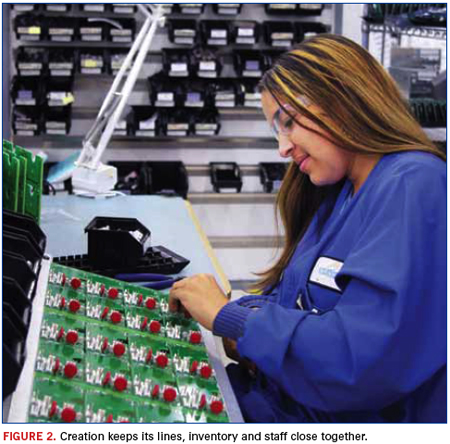
The Creation factory layout is atypical of most. While it follows a cell model that others (Plexus for one) have long since adopted, those cells are based on the customer, not the equipment or the engineering team. So while the Oak Creek, WI, factory, for example, has three common SMT lines (although the equipment set was all over the map: DEK screen printers; Juki, Universal and Fuji placement machines; Heller 1800 EXL and Vitronics-Soltec XPM2 reflow ovens, and an Electrovert Aquastorm 200 for cleaning) located in the center of the 90,000 sq. ft. building, customers have their own cells around the perimeter of the lines. Each cell is labeled with the customer name (dangling by a placard), its own 5S scorecard, customer surveys, and a client history. Most inventory is located at the point of use. Stencils are sited on the factory floor adjacent to the lines.
Each line has an LCD display showing work-in-progress and loading information. The platform is based on a color-coded system, compiled in Access, that all manufacturing staff have access to. A Kanban system tracks inventory on the floor.
Commenting on the unusual layout, Hyatt said, “It’s important for our teams, and we like the visual identity. Anyone can tell at a glance what’s running and what’s not.”
Every Creation factory has conformal coating capability, and in Oak Creek we also saw x-ray, functional test, and an Agilent 3070 ICT. To optimize space, a second story hangs over part of the floor, used for parts storage. A clean room, engineering lab and a dedicated NPI section round out the picture.
Home Field Advantage
Even while expanding the operation in China, Creation has been looking at possible acquisitions in a low-cost region (read: Mexico) in the Western Hemisphere for a few years, writes Tymos, who regularly blogs and tweets. The Aisling acquisition stretches the corporate footprint but takes advantage of the proximity and labor rate advantage of Mexico. Creation is relocating the manufacturing operation to a newer 125,000 sq. ft. facility.
While I haven’t seen any direct indication that OEMs are broadly dissatisfied with China, after a decade of waning US manufacturing, the pendulum is swinging back, and Creation Technologies is in good position to take advantage. “That we’re largely a North American company seems to resonate with customers, especially in this day and age of ‘offshoring and outsourcing,’ ” Hyatt allows.
Creation Technologies is a North American manufacturing success story. But it’s more than that. It is also the CIRCUITS ASSEMBLY EMS Company of the Year.
Mike Buetow is editor in chief of CIRCUITS ASSEMBLY (circuitsassembly.com); mbuetow@upmediagroup.com.
Design considerations for moving from 0.5mm pitch to 0.4mm pitch and below.
Package-on-package is a method of stacking components atop one another. Some OEMs use PoP to reduce the board real estate area, particularly for small handheld products and devices. Others are moving to PoP because end-markets demand greater performance in smaller systems and products. In either case, OEMs will find that there’s a game changer going from 0.5mm pitch BGA PoP to the next generation, 0.4mm ultra-fine pitch BGA PoP.
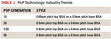
Industry trends say that PoP-populated PCBs will evolve in three stages as shown in Table 1.
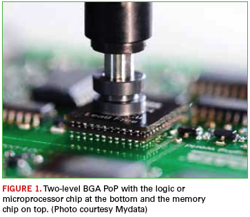
Currently, in some camps, PCB designers are at the first stage using two-level BGA PoP with the logic or µP (processor) chip at the bottom and the memory chip on top (Figure 1). However, there are certain key steps involved in increasing success at the third level. But first, before stepping out with 0.4mm pitch BGA PoP-based PCB designs, it’s important to revisit those rules-of-thumb at the 0.5mm level and above. These rules-of-thumb relate to pad sizes and solder mask openings up to 0.5mm pitch.
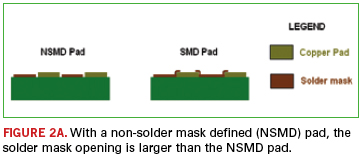
First is to maintain pad size around 85% of the ball size of the BGA. Second is to provide a non-solder mask defined (NSMD) pad whereby the solder mask opening is larger than the NSMD pad (Figure 2a). Typically solder mask is opened to a diameter of around the ball size of the BGA. In this instance, the solder mask is recessed, permitting it to provide stress relief to the NSMD pad during reflow. In short, it creates a protective dam so that solder can go around it.
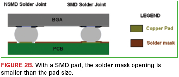
Further, since there are no existing published design guidelines for 0.4mm pitch PoP-based PCBs, be wary of today’s conflicting reports. Issues stemming from these reports deal in large part on PCB pad sizes and solder mask openings. Take, for example, a 0.4mm pitch BGA PCB design using NSMD pad sizes, where in a low-volume run the results were highly acceptable. However, for larger production, this approach produced low yields. By adopting the solder mask defined (SMD) pad approach (Figure 2b), whereby the solder mask opening is smaller than the pad size, better yields and results are achieved. Also, it’s important to note when deploying NSMD pads for 0.4mm and 0.3mm pitch BGA/PoPs, the chances are great of creating bridging between pads due to insufficient solder mask webbing between pads.
Key Factors to Pursue
Since 0.4mm pitch BGA PoP-based PCB design is in its infancy, it is a good idea for the PCB designer to perform preliminary experimental layouts and prototype rounds to get the lay of the design before launching into a full-fledged layout. Rules followed for 0.5mm pitches may not work for 0.4mm cases at high volumes. Typically, ball sizes of 0.4mm pitches are smaller. Reducing the pad size by another 15% may make the solderable area insufficient. Second, using NSMD with 0.4mm parts may cause bridging between adjacent pads. Third, since the pad sizes are so small, and there is no solder mask webbing to provide adhesive strength, it may peel off during reflow or in the field.
Against this backdrop, there are six key factors affecting the reliability of a 0.4mm ultra-fine pitch BGA/PoP-based PCB design. Those are pad design, via-in-pad guidelines, via finish, stencil design, solder paste, and thermal profile.
As suggested, SMD is the pad of choice for 0.4mm pitch. In this case, the pad is created as the same size of the BGA ball. Solder mask opening is around 15% less than the ball diameter. Here, the solder mask laps over the edge of the copper pad to strengthen the connection in a couple ways: One, it strengthens the bonding between the copper and the PCB’s laminate; two, with the copper pad going farther into the solder mask, copper area is larger. That larger copper area provides a greater surface for the PCB laminate to adhere, making the connection twice as strong.
Also, in these designs, traditional BGA dogbone fan out used for larger pitches with extended real estate is not considered at all. Instead, via-in-pad is used, a specialized technique for escape routing fine-pitch BGAs. Before discussing guidelines for use, it’s a good idea to revisit the via-in-pad approach. This escape routing technique involves vias being placed directly on the BGA pads and filled with a conductive or a nonconductive material, which provides a fairly flat surface. Traditionally, silver was used to fill the vias, and a small increase in density was realized so that the designer could route a few more signals on the outer surface. That technique has evolved considerably, and now the materials of choice fall in the nonconductive category. The reason: Vias filled with a nonconductive epoxy perform better because the coefficient of thermal expansion (CTE) is comparable with that of the PCB.
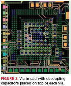
Therefore, the rate of expansion is similar to the board material, allowing for a more reliable joint. Issues like via out gassing and solder voids can be avoided. The same method of filling vias is used on 0.4mm PoP designs. A key point to make is that whenever there are vias below a BGA and available for connection, they should be filled, tented, or capped. Otherwise, they can cause voids and out-gassing during reflow. Also, as shown in Figure 3, discrete decoupling capacitors can be placed directly over the vias on the bottom side. This provides a low inductance path to the power system.
Place and Route
When it comes to 0.4mm pitch BGA PoP, it’s not a good idea to place a BGA on the opposite side of another BGA, which is the typical case in 0.5mm pitch BGA and above. Instead, BGA/PoPs should be placed offset from each other with about 500 mils spacing to maintain board level reliability and ease of debugging on the bench when needed.
Again, since 0.4mm pitch BGA/PoPs are so new, manual routing is recommended over autorouting. Reason: An autorouter is a computer program based on mathematical algorithms and fixated on making connections. It doesn’t think like a human designer. In most instances, using the autorouter results in unusual traces, many unnecessary vias routed and many unnecessary loops.
In effect, the autorouter creates more vias than are required, thus reducing the reliability of the final assembly. Also, those extra vias add discontinuities if the design calls for certain impedance requirements. Typically, impedance is based on the geometry of the connection from driver to receiver. Hence, that impedance path needs to be uniform. Whenever there is a via, there is a discontinuity in that uniform pad, and impedance changes at that particular moment. Ideally, for a 0.4mm pitch BGA/PoP-based design with high-speed signals, you don’t want a via. Additional vias will cause considerable discontinuities and subsequent ringing and reflections.
While performing the routing, it’s also vital to avoid creating heat sinks. How can a designer inadvertently do this? This occurs when a trace is put on a via or a dogbone fan out is performed from a via that’s almost the same size as the pad. The result is the traces and vias pull heat away from the BGA/PoP and cause issues during assembly. In another example, copper pour is placed over BGAs. This may happen when there are multiple power/ground pins on the device. During assembly, this arrangement will sink the heat during reflow and cause cold solder joints, resulting in opens or intermittent connections.
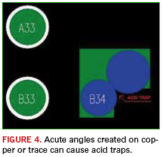
Also, in the realm of routing, acute angle traces should be avoided when connecting BGA pads, as they could result in acid traps. Acid traps are acute angle areas or small areas where etching chemicals get stuck, and eventually, those small chemicals eat away the traces and intermittent connections result (Figure 4). Finally, the designer should design with metric units rather than English for fine-pitch BGA devices and PoP. This will not only increase accuracy, but will also avoid requiring four decimal places of accuracy when converting from micrometers to mils.
Team Effort
There’s always talk about working together to successfully complete a project. But in the case of 0.4mm ultra-fine pitch BGA/PoP-based PCBs, there is no question it is essential that the PCB designer, fabricator and assembler work in unison, with the designer taking the lead. The PCB designer must maintain regular discussions with the fabricator to understand its capabilities, such as determining whether it can handle certain minimum hole size aspect ratios. Part of that dialogue includes understanding the spacings for a high-speed design’s impedance control traces, and knowing the chosen substrate material’s capacity to handle those requirements.
Furthermore, the designer must have a good handle on a fabricator’s manufacturing limits. Those can be divided into three categories: standard technology, high-yield, and engineering development. The first refers to a fabricator’s capability, for example, 5 mil traces and spacing, which is a midrange capability for most board shops today. For mass production, high yield is typically 8 mil lines and spaces. (These numbers are relative, so for some fabricators, 10 mils will be high yield, while 8 mils might be typical for others.) Third, there’s the engineering development category. This deals with a fabricator’s highly advanced capabilities, which fall into the 2.5 mil traces and 2.5 mil spacing class.
The layout designer must also know the assembler’s capabilities, such as the minimum pitch that assembler can work with. Either it can or cannot perform 0.4mm ultra-fine pitch BGA/PoP PCB assembly. If it is building 0.4mm pitch, what kind of solder paste are they using? Are they following manufacturer’s recommendations on the reflow profile? The designer must also have discussions with the paste manufacturer to ensure the right pad sizes are associated with the right solder paste.
Avoiding warpage is another key area demanding close interaction between the designer and assembly. By not paying special attention in this area, excessive warpage can result in bridging, solder slumping, head in pillow, or opens.
PoP is an emerging technology, and will be utilized more as the industry gears toward further miniaturization of the existing technologies. Do not assume that the same techniques that work for larger versions will necessarily scale to the smaller ones.
Syed W. Ali, C.I.D+ is a PCB layout engineer at Nexlogic Technologies (nexlogic.com); info@nexlogic.com.

Press Releases
- Zollner Puts a New Mechanics Building into Operation
- Changes in Incap’s Management Team: Incap updates its leadership model to support its growth strategy
- Niche Electronics Celebrates Completion of Florida Expansion
- Microscreen Names Nik Thomas Director, Expands Leadership Role Amid Continued Organizational Growth