


Reducing solar silver costs using a dual-print process.
More than a year ago I wrote of the use of certain printing strategies to help offset the high cost of silver (“Solar Strategies to Offset the Rising Cost of Silver,” CIRCUITS ASSEMBLY, September 2011). These ranged from the advancing accuracy of screen technology and metallization print platforms (which, by the way, have already helped reduce silver paste volume requirements) to print-on-print and dual-print techniques, to a complete change in materials. At the time, these were proven approaches to silver reduction, but I had no practical figures to share. Now I do.
Recently our company partnered with DuPont Microcircuit Materials, a leading manufacturer of photovoltaic metallization pastes, to analyze potential cost-savings and cell conversion efficiency improvements in the manufacture of c-Si solar cells. The cost savings centered on silver paste consumption reductions, a central focus in the photovoltaic market for some time. With silver prices at $1300/kg at the time of our study, cutting cost was more important than ever. The drive to reducing silver use has already led to more efficient grid architectures, including the design of narrower finger widths, moving from the 80 to 90µm range to widths of 50 to 60µm in production. Printing these finer dimension fingers has been achieved through advances in paste technology, print platform capability and improvements in screen production with ultra-fine meshes. However, paste laydown reductions have resulted in thinner busbar paste volumes, so one must be careful to balance this so that subsequent solder adhesion (during the attachment of tabbing ribbons) is not adversely affected.
The work with DuPont MCM utilized several components to analyze single- and dual-print processes and their relative effectiveness in relation to paste reduction, cell reliability and cell efficiency. These elements included DEK-manufactured ultra-fine mesh screens, both traditional and optimized DuPont MCM silver metallization pastes and DEK electroformed nickel stencils. With the single-print process, standard mesh screens were used to print the cell rear side, and ultra-fine mesh screens were used for the front-side grid in total (fingers and busbars) with a latest-generation front-side paste. Using ultra-fine meshes in single-print mode permitted the desired reduction in paste consumption – as much as 30% in this evaluation – as well as slight increases in electrical efficiency but, as I cautioned, did result in reduced solder adhesion forces. Because a finer mesh was used, the busbar area was printed thinner than the minimum required for good adhesion. So, with a single print scenario and ultra-fine screens, we achieved what I would call a win-win-loss: reduced silver paste consumption (win), slight improvements in electrical efficiency (win), and reduced solder adhesion (loss).
Taking the analysis further, the next phase leveraged dual-print techniques to find out if paste laydown reductions, cell efficiency improvements and good solder adhesion could be achieved. For this evaluation, busbars were printed with an optimized – or floating – busbar paste through a 400 mesh (400 wires per inch) screen. The advanced busbar paste is non-contacting and enables the busbar to do its job (conduct current away from the fine lines) and mechanically adhere to the wafer surface without making electrical contact with the wafer itself. Therefore, with the optimized busbar paste – as opposed to the traditional front-side grid paste – less paste can be used without adversely affecting adhesion. In fact, in our evaluation, the optimized busbar paste actually increased adhesion force beyond the normal standard. Next, specialized dual-print electroformed stencils, 30µm thick with 30µm apertures, were used to print the fine finger widths with a standard front-side paste. Because the stencil design permits a 100% open area in the apertures (as opposed to mesh screens), extremely fine lines can be achieved and, therefore, paste consumption reduced further. So, here we have a win-win-win scenario: a relative increase in cell efficiency of >0.5%, reduced paste consumption of up to 40% and higher reliability modules due to the improvement in solder adhesion forces.
With the dual-print process, the rear side is printed, followed by the screen print of the front-side busbars and then the stencil print of the front-side grid/fingers.
With the extra print step, an additional printer is required. But, a detailed cost of ownership analysis reveals that even with the extra equipment costs, the dual-print processes as outlined above yield significant cost savings. Our calculations show that with the dual-print scenario described here and a consistent cell efficiency of 17.25% (note that this assumes no increases in efficiency, although our work showed a greater than 0.5% relative efficiency gain), a cell manufacturer would save $120,000 per year, even taking into account the cost of the additional printer and stencils.
With all the pressure to reduce manufacturing costs and lower the overall price tag of solar power, the results of this work are a tremendous step forward. This is arguably the best current solution for silver paste consumption reduction – one that also improves efficiency and enhances reliability. And work is already underway to advance stencil technologies for, perhaps, a single print solution with similar results. I’ll keep you posted.
For more information on the study conducted by DEK and DuPont, please contact the author.
Tom Falcon is a senior process development specialist at DEK Solar (dek.com); tfalcon@dek.com. His column runs bimonthly.
Several important process and equipment revelations were made at the annual Pan Pac symposium.
The 18th annual Pan Pacific Microelectronics Symposium took place Jan. 22-24 in Maui, HI. The conference brought together the industry’s top specialists from North America, Europe, Asia and Australia to share the most up-to-date science of electronics manufacturing and reliability. Technical papers and presentations covered a diverse range of electronics topics, including silicon interconnects and packaging, embedded devices, PCB assembly and cleaning, failure analysis and reliability models.
The Best Paper honor was awarded to Rolf Aschenbrenner, Ph.D., Fraunhofer Institute for Reliability and Microintegration, for his paper, “Panel Level Packaging – A Manufacturing Solution for Cost Effective Systems.” The paper highlighted some of the challenges in embedding high I/O power chips, including heat removal, electrical isolation and molding processes. This is a distinguished honor, as the award recipient is determined by the conference attendees.
Some of the SMT-related presentations of particular interest to Circuits Assembly readers included:
- Asymtek’s Horatio Quinones reviewed the latest advances in fluid jetting technology, highlighting the breakthrough of jetting Type 4 solder pastes. Until now, jetting has been performed with the finer powder Type 5 pastes, which bring reflow challenges like graping and balling. Larger particle size pastes were notorious for clogging jet seats after only a few shots. New jetting systems are able to produce very fine lines at speeds of up to 100mm/sec with no clogging. Applications include adding extra solder paste for RF shields, pin-in-paste reflow, BGA corner balls or SMT joints subject to frequent mechanical stresses, and dispensing paste for very fine feature components, MEMs lids or cavity PCBs.
- Kyzen’s Tom Forsythe presented new findings on cleaning that change the way we look at low-standoff components. Gap height is emerging as a significant factor affecting cleanability. As IC packages get miniaturized, gap height shrinks, creating new challenges for cleaning underneath the components – many of which were designed for no-clean soldering only. Forsythe presented the results of a sizable DoE to unlock the secrets of cleaning low-gap chip scale packages; it characterized the effectiveness of three cleaning solutions at five concentrations and four temperatures on two solder paste formulations. A lot of really good data to digest.
- Universal instruments’ Martin Anselm gave a fantastic overview of the PCBA failure analysis process, breaking it into four areas of investigation: material quality, assembly process, design and reliability. Anselm’s presentation was a summary of the three-hour class offered at the annual SMTAI conference, which contains valuable information for anyone in SMT production or new product engineering, as well as quality and SQA. The knowledge of how solder joints fail, what makes them fail, and the circumstances under which they fail is a powerful intellectual tool for people involved in PCB design, assembly or inspection processes.
- Northstar Imaging’s Wes Wren opened our eyes to state-of-the-art x-ray imaging. After explaining the difference between contrast and resolution, and the implications of tube-to-detector distance, he blew away the audience with images of new 4D tomography. The fourth dimension is the time domain, and the x-ray videos of real-time processes, like welding or the movement of a rack and pinion, are amazing. Go to www.xviewct.com/industrial-ct-news/news-items/taking-3d-x-ray-inspection-to-a-new-dimension-4d-computed-tomography to see some really cool videos.
- Tom Borkes gave us a lesson in economics that we all can use: realistic cost bases for PCB assembly in various world regions, and ideas on how to compete on a global scale. His analysis included labor, materials and a discussion of nations’ predispositions for off shore manufacturing. The paper introduced a noteworthy acronym: DF MATERS. That’s Design For: Manufacturing, Automation, Test, Environment, Reliability and Service.
- Nihon Superior’s Keith Sweatman introduced nanosilver particles that sinter themselves together at 150°C. In fact, they have such an affinity to self-sinter, the particles need to be protected by a passivation coating. They are less than 100nm or 300 atoms wide, and can be used in a variety of applications, including replacing high-lead solders in semiconductor die attach. They have good electrical and thermal conductivity and have been proven reliable, even in high-temperature operating environments. Solder pastes incorporating nanosilver have many different uses, are usually tailored to the application to address specific processing or performance characteristics.
In addition to the discussions of new technologies and methods, many general industry updates were provided, including Dieter Bergman’s review of IPC standards development, Chuck Bauer’s overview of new and novel interconnect technologies, Chuck Richardson’s iNEMI roadmap, and Wei Koh’s keynote address on China’s semiconductor development efforts.
The Pan Pacific Microelectronics Symposium is a three-day, single track conference that gives experts from across the industry and around the world the opportunity to learn from and inspire each other. It is made possible in large part by corporate sponsorships from Kyzen, Libra Industries, SonoScan, Indium, Nihon Superior and Nordson. The SMTA organizers and attendees sincerely appreciate their support.
Next year’s conference will be held Feb. 11-13, 2014 on the Big Island of Hawaii, and the call for papers is now open.
Chrys Shea is founder of Shea Engineering Services (sheaengineering.com); chrys@sheaengineering.com.
How to adjust an oven so a single recipe will work across multiple ovens for an individual product.
The ability of equipment to produce good product is fundamental to every manufacturing process. The ability to quickly setup and run a product on different process lines can make the difference in being able to satisfy a customer’s requirement, missing a delivery date, or making a profit. This process line flexibility requires good equipment with repeatability between lines to be a success. To do this, the process engineer needs to maintain their equipment to high standards and understand its capability.
In the 1950s, Wendell Abbott of GE wrote a detailed paper about the distribution of a measurement within a lot of material (or machine) and among lots of material that described the interactions. Although his paper is complicated, the concepts of variation within one oven and among different ovens are important when discussing flexibility across multiple SMT process lines.
Up until recently SMT process engineers with multiple process lines established a different recipe for each reflow oven because of variation between equipment. With modern technology and control systems, it is possible to adjust some reflow ovens so a single recipe will work “among” ovens for an individual product. Once this is done, repeatability among ovens becomes a process tool that saves time and makes production easier. To be comfortable with control among ovens, we first need to discuss the variation within an oven.
Repeatability within an Oven
Engineers are often asked how well their process meets a manufacturing specification. Phrases such as “nearly all the time” or “the majority of the time” are not acceptable in a technical world; thus establishing quantifiable data with measurable attributes is important. Placing a measurement or number on the ability of a process to meet a specification has evolved to what is known as process capability. This process capability measurement establishes a ratio of the process variation to a specification and is expressed as Cp or CpK.
It would be simple if we could make a single measurement of the process and compare it to the specification, but real life is not simple. Processes have variation that needs to be quantified before we can make a statement about how good they are. It takes multiple samples and math to quantify process variation. If we want to be 100% confident of the variation of a process, we would need to measure every piece. But that is impractical, so we use sampling and statistics to estimate the variation in a process. As you can guess, choosing the sample size becomes an issue of time and cost verses the accuracy of the data. We do not intend to turn this into a statistics course, but will give a simple overview of the concepts and how they can be applied to an SMT reflow oven.
Since process capability is a comparison of the process output to a specification, both need to be identified. In the case of a reflow oven, the specification is usually the reflow profile supplied by the paste manufacturer. It consists of ramp rates, soak time to traverse specific temperature ranges, time above the liquidus of the solder, and peak temperature.
The process output includes two pieces of process data for each specified attribute. The first is the average and the other is the standard deviation. The average is simple math (addition and division), while calculating the standard deviation is more complicated. Spreadsheets, statistical programs and some calculators can do the analysis without the need for manual calculations. (Consult statistical handbooks and texts for a detailed explanation of standard deviation.) What process engineers need to know is the standard deviation of sample data can predict the process variability.
The process to specification ratio can be expressed in two ways: One is called Cp and the other is CpK. The difference is that Cp focuses on machine capability, while CpK focuses on the process for an individual product. Cp uses the tolerance range and standard deviation without regard to the actual target to determine if the machine has the ability to make good product. The tolerance range is usually set to an industry standard. On the other hand, CpK uses Cp calculations and the actual target to ensure the process meets the specification for an individual product.
The calculations are:
Tolerance range = upper specification limit minus the lower specification limit
Cp = Tolerance range / 6 times the standard deviation
CpK = Cp times (1 minus K)
where K = the absolute value of the target minus the mean / by ½ the total tolerance range
Let’s say that we have the following peak temperature data:
The specification given by the paste manufacturer is 240 ± 10°C.
Therefore, the target is 240°C with a tolerance range of 20°C.
After running 10 profiles, we found that the average peak temperature
is 238.5°C.
And the spreadsheet calculations tell us that the standard deviation is 0.34.
Therefore, the Cp would be 20 / (6 X 0. 34) = 9.8
K would be (240.0 – 238.5) / 10 = 0.15
Then the CpK is 9.8 X (1-0.15) or 8.33.
Statisticians note that when the machine capability (Cp) is 2.0 or greater, we have a capable process, regardless of the process center. They also say that for a process to be in control, the CpK has to be 1.33 or greater, accounting for the process center. In this case the Cp and CpK are excellent.
To help make it clear, we can look at the following figures. Figure 1 depicts a perfectly centered process with the target and process average equal to each other. The statistical process variation is well within the specification limits and has a 1.33 CpK. This allows for some movement of the average, while the product remains within the specification.

Figure 2 shows a centered process, but the variation is larger than the specification limits. When this happens, the process is producing conditions that are out of the specification window. In this case, the CpK is about 0.8.

Figure 3 shows two processes that have variation less than the specification limits, but they are not centered. While the Cp (not considering the target) would be good, the processes are producing conditions that are out of the specification window. If they were centered, they would be OK. The CpK in these cases is about 0.85.

Now let’s look at the results from a study of an actual reflow process conducted over a five-day period. Profiles were taken each morning and afternoon on a 10-zone BTU Dynamo reflow oven running a Pb-free solder recipe. The product was a 350g board with six thermocouples attached to critical components.
The ramp, time above liquidus (TAL) and peak temperature data from each run were put in a spreadsheet to calculate the averages and standard deviations. The results are in Table 1.
Comparing results to the Pb-free solder specification, we see the averages are very close to the target (Table 2). This indicates the recipe is correct for this product, but does not indicate the process variation. Not knowing the variation reminds us of the guy who had one hand in boiling water and the other in an ice bath; he was uncomfortable, but on the average, the temperature was OK. Thus we need to know the variation of the process. Since we are taking a sample and not measuring the profile for every part, we can use the standard deviation of our sample and the formulas previously discussed to calculate the CpK.

This indicates that the process run on the third over 3 is in statistical control, because the CpKs are all above 1.33. If the process specification is correct, the reflow process is making good product. (Note: This study was conducted over a five-day period, but the same can be done with 10 consecutive runs or 10 runs in one day.)
Repeatability among Ovens
Now that we know one oven is in control, how do we show that the process is in control among multiple ovens with the same recipe?
We could obtain a single profile on a second oven to show that it is within the process widow identified by the paste specification. But that would not verify that the second oven had the same process variability as the first, and we could be deceiving ourselves into thinking the process was in control. The answer is again in statistics and CpK.
We could complicate our decision making with statistical evaluations such as the student t-test1 and Mr. Abbott’s calculations, but it is possible for the process engineer to keep it simple by comparing the results of CpK calculations on multiple ovens to show there is repeatability between them.
Before we start the 10 runs on the second oven, we need to fine-tune or adjust the profile by using thermocouple offset in the oven control program.
To obtain the offset, we run a few profiles on the second oven and compare it to the averages we produced on the first oven. We are tuning the oven, not calculating the CpK. Although we could get more accurate data with multiple runs on Oven 4, we chose three runs in an effort to save time (Table 4).

The peak temperature and TAL are slightly lower on Oven 4, so if we use an offset in the oven control of 3°C to increase the peak temperature, the TAL should be slightly longer.
Then obtaining profile data with the offsets from 10 runs and calculating the averages, we get the results in Table 5.

The small differences in the averages between Oven 3 and Oven 4 tell us that we chose the correct offsets.
Then, using the same process specification as Oven 3 and the standard deviation from Oven 4 data to calculate the CpK on Oven 4, we get the results in Table 6.
Both the comparison of the averages and CpK confirms that Oven 3 and Oven 4 are in control with the same recipe.

Table 7 shows the same for yet another oven (identical product, set points, offset procedures, and specification limits).

Therefore, we have three ovens using the same recipe that are all in control. This allows us to say we have repeatability among them.
Let’s do a quick review by comparing the data from the three ovens (Tables 8 and 9). The first thing we see is that the rising, falling, TAL and peak temperature averages are very close to each other; thus we have the correct tuning offsets. The second and most important is that every specified attribute is within control because the CpKs are more than 1.33.


We have proven that we have repeatability within each oven and among the three ovens, and the process engineer can be confident that they can produce good product in any of the three reflow ovens.
End Notes
1. A t-test is any statistical hypothesis test in which the test statistic follows a Student’s t distribution if the null hypothesis is supported. It can be used to determine if two sets of data are significantly different from each other, and is most commonly applied when the test statistic would follow a normal distribution if the value of a scaling term in the test statistic were known.
Fred Dimock is manager, process technology at BTU International (btu.com); fdimock@btu.com.
Next-generation materials make almost every stencil better.
Once in awhile, something really big comes along that makes a step function improvement in our PCB assembly processes. Stencil printing has enjoyed its share of milestone moments, and it’s currently on the brink of another. The science of surface energy modification is enabling a new level of print quality, and it is poised to make a significant impact on the process, on the same order of magnitude as electroformed stencils did in the 1990s or structured light SPI in the 2000s.
Commonly known as “nanocoating,” the process of applying a single-molecule layer of material to the stencil’s contact side dramatically lowers its surface energy and improves solder paste release. Several types of materials are classified as nanocoatings; the most popular is the two-part system introduced in 2010. Originally met with overt industry skepticism, the coating quickly proved itself in independent tests and developed a strong user base. I admit that I was one of the doubters who was quickly converted by the overwhelmingly positive data; the coating made almost every stencil tested perform better, and prompted an instant 5% overall print yield increase when implemented in production.1,2
The original formulators have now introduced a next-generation nanocoating product that improves printing performance, along with a new business model that makes it more affordable and more available. Eric Hanson, Aculon’s vice president of technology, presented the science of how and why the technology works at the technical conference, while Edward Hughes, Aculon’s CEO, discussed supply-chain improvements on the show floor. I was able to speak with both, and they answered many of the questions that process engineers and printing specialists have been asking each other for the past two years.
What is it and how does it work? The coating is known as a Self-Assembling Monolayer of Phosphonates, or SAMP material (sidebar). These films are literally one molecule thick. They don’t change the surface roughness or topography; they change the surface energy. SAMP surface coatings are engineered to produce specific properties; they may be hydrophobic (water repelling), oleophobic (oil repelling) or fluxophobic (flux repelling).
The ultrathin (<5 x 10⁻⁹m) coating prevents flux from wetting out on the stencil. Poor wetting equals poor adhesion, so in the solder paste tug-of-war of stencil-PCB separation, the stencil quickly loses its grip on the paste. The minute “strings” of paste that would stretch between the stencil and the PCB as the two separate break free from the stencil, rather than snap back to it, keeping its underside cleaner. The flux-repellent surface also prevents solder paste from wicking out around the edges of the apertures during the print stroke,3 further limiting bottomside paste buildup. The cleaner contact surface results in better gasketing, less squeeze out, and crisper print definition.
How can a user tell if the coating has worn off? This has been a major concern since its introduction. Nobody wants to wait for performance drops to signal time for reapplication. The solution is a dyne pen: a felt tip marker filled with dyne fluid. It’s a basic go/no go gage; if you swipe the marker across the stencil and the fluid beads up, the coating is still robust. If the mark doesn’t bead up, it’s time to reapply.
In the laboratory, more quantitative indications of surface energies are acquired by measuring the contact angles of oil and/or water on surfaces. Higher surface energies produce good wetting and lower contact angles; lower surface energies produce poor wetting and higher contact angles. Untreated stencil foils exhibit oil contact angles of approximately 10˚, whereas treated foils exhibit oil contact angles of approximately 87˚.
How long does the coating last? The coating is designed for durability. Users of the original formulation cite reapplication intervals of 25,000 wipe cycles or more, a very long time for many print processes. Given that one of the prime benefits of this treatment is extending wipe frequencies, 25,000 wipe cycles could become a very, very long time.
At Apex, Hanson presented results of multiple durability tests, including one that demonstrated robust coating presence after 100,000 abrasion cycles, outlasting vacuum deposited nanocoatings as shown in Figure 1.4

Will stencil cleaning solvents attack the coating? No. The new coating has been compatibility tested with one major manufacturer of stencil cleaning chemistry and is currently undergoing testing with another. Single application coatings have withstood 160 15-min. cleaning cycles in typical stencil cleaning chemistries with no degradation in repellency. That’s equivalent to cleaning it once every day for almost six months, which is more cleaning than most stencils see in their lifetime. If stencil cleaning processes use solvents that have not yet been tested and approved, chemistries with a pH <9 are recommended.
What’s the new performance improvement? In addition to reaching new levels of durability for nanocoatings, the new formulation is reported to improve fluxophobicity, as it is 50% more concentrated than the original. The extra “slipperiness” of the stencil should extend underwipe frequency intervals even farther than its predecessor. Users testing the new SAMP reported incredible – almost unfathomable – results: 40 prints per wipe on 0.5mm µBGAs, as shown in Figure 2. Hanson comments on the performance feedback: “We understand PCB assemblers’ needs for better print quality, and are extremely pleased that this product makes such a remarkable improvement in the overall process.”

When testing the original formula with Vicor’s Ray Whittier in 2011, we didn’t test for wipe frequency, but found an enormous impact on print yields,5 as shown in Figure 3. We tested 13 pairs of stencils of varying composition and quality, and it boosted yields on all but two pairs. (Note that those were seemingly beyond help, originally producing only 0 and 20% yields.) The results were so dramatic that Whittier immediately implemented the coating as the Process of Record, applying it to all stencils in his operation. We have plans underway to test the new coating formulation on a similar test vehicle and quantify the performance differences.

Can it be used on any type of stencil? Yes, the coating bonds to metallic oxides, and is compatible with electroformed, electroplated or laser-cut nickel, as well as the many stainless steel alloys available. (As an aside, I just finished another big stencil study in which laser-cut SS outperformed electroform for the third time in as many years.)
Does it actually coat the aperture walls, or just the bottom surface of the stencil? The product volume is formulated to treat both the underside and the aperture walls. The company developed an instructional video in which Hanson demonstrates the application process and offers tips for achieving optimum coverage (aculon.com/stencils.php).
Does it contain ionic materials that could pose reliability risks to solder joints? No. When properly applied, the cleaner/treatment chemistries will not contaminate downstream processes. While the cleaning solution does contain some ionic materials, they are removed during the rinsing step with water. The monolayer treatment step does not contain any ionic materials that could compromise subsequent processes.
What’s the cost per stencil? The cost of the two-packet system has been reduced from $40 per stencil treatment to $25. At $40, I thought it was a bargain because it was still less expensive than reworking a single BGA with a print-related solder defect. At $25, the deal just got sweeter and the ROI faster. One user quantified the payback period in wiper paper alone: about 170 wipes with standard paper, or one roll of the really good stuff. I want to apply it not only to my stencils, but also to my board support tooling and squeegee blade holders to make them easier to clean on changeovers.
The two-part coating system is available to stencil manufacturers and PCB assemblers, giving the latter the option to specify it on their stencils or apply it themselves. Because all parties have equal access and pricing, assemblers should expect a service fee if the stencil shop applies it. The application process is pretty straightforward; details are in the video.
With two years of limited distribution under its belt and a loyal following of users, SAMP-based stencil nanocoating is ready for prime time. It’s going to change the way most operations manage and control their printing processes over the next few years. But unlike some of the previous breakthrough technologies that advanced stencil printing, it doesn’t come with a hefty price tag or a steep learning curve. It’s $25, plug and play. This coating’s low price, widespread availability and ease of use may quickly make it the de facto standard for all SMT stencils.
What is SAMP Technology?
Self-Assembling Monolayer (SAM) materials are specially designed molecules that automatically organize themselves and bond to form engineered chemical structures, without requiring any catalysts or forming any byproducts. The molecules have head and tail groups; the head groups bond to a substrate, while the tail groups bond to each other and deliver the desired functionality.
Phosphonates (P) are organic compounds that bond readily with metal oxides to chemically “seal” surfaces, and are commonly used to inhibit corrosion or scale because they are extremely stable in harsh environments.
The SAMP molecule developed specifically for stencil nanocoating consists of a phosphonate head group that covalently bonds to the oxides on the stencil’s surface and a specially selected tail group designed to repel nearly all flux formulations. The molecules set up and form a single-molecule layer within seconds of their application. Familiar SAMP applications include surface treatments for sunglass and optical lenses, PDA screen cleaners, watch displays, nozzles and needles.

References
1. Chrys Shea, “SMT Stencils from a Production Perspective,” CIRCUITS ASSEMBLY, December 2011.
2. Chrys Shea, “What Used to be Old is New Again?” CIRCUITS ASSEMBLY, February 2012.
3. C. Ashmore, M. Whitmore and J. Schake, “Big Ideas on Miniaturization,” Proceedings of IPC Apex Expo, February, 2013.
4. R. Bennett, Ph.D., and E. Hanson, “Low Surface Energy Coatings, Rewrites the Area Ratio Rules,” Proceedings of IPC Apex Expo, February 2013.
5. Chrys Shea and Ray Whittier, “Evaluation of Stencil Materials, Suppliers and Coatings,” Proceedings of SMTA International Conference, Fort Worth, TX, October 2011.
Chrys Shea is founder of Shea Engineering Services (sheaengineering.com); chrys@sheaengineering.com.
Benchtop was in and integration was all the rage at the annual North American trade show.
At IPC Apex Expo this year, small was big.
The annual trade show, the largest assembly equipment event of its kind in North America, kicked off in late February to strong crowds and a positive vibe that belied the unseasonable chill in the San Diego air.
A number of products were introduced that will challenge previous designs for market share. Universal Instruments, Panasonic, Europlacer and Fuji were among those with new placement machines. Speedline showed the latest Camelot dispenser and Momentum printer, both of which are smaller than previous models. BTU proudly discussed Dyanmo, a lower wattage, smaller platform for convection reflow soldering. On the test and inspection side, several benchtop analyzers and testers were unveiled by companies big (Agilent, CyberOptics) and small (ASC).
As with last year, sensors and lasers are all the rage. Precision and speed often improve on different curves, and judging by the new machines this year, the current emphasis is more on the former. And many equipment vendors have retooled their offerings for the high mix, high complexity market.
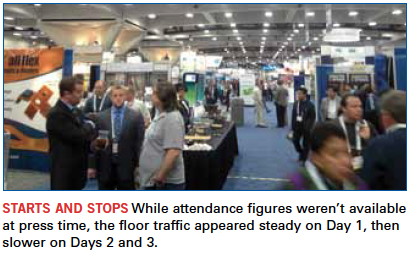
Floor traffic, always the arbiter of a show’s success, appeared steady throughout the first day, never overwhelming but always busy and noisy. The second day started slower than the first before picking up in the late afternoon, giving exhibitors more time to dwell on the state of the industry economy. Day 3 was fairly quiet.
Several exhibitors noted that visibility remains clouded for 2013, with those supplying to the automotive sector the noticeable outliers. David Wolff of bare board distributor NCAB noted a change in supply chain practices, saying that OEMs are “absolutely taking control of (bare) boards again.”
Software
Aegis very proudly rolled out FactoryLogix, a software suite aimed at coordinating the entire manufacturing enterprise outside of accounting and R&D, including box build and system integration. The new suite tracks NPI progress, and can be adapted to individual manufacturing sites around the world. It also handles mechanical CAD as well as EDA. And, it’s configurable, but doesn’t require programming. As president Shaun Black explained, “We wanted to get the customer integration costs – such as coding – out, and the configuration in.”
Printing/Dispensing
PVA rolled out the VPX-2K 2-component dispensing pump.
Speedline’s Momentum Compact printer shrinks the footprint of the previous generation. And its new Camalot Prodigy has a narrower footprint but loses none of the functionality, boasting a 30µm accuracy at full system speed, and coming in single or dual lane versions.
DEK refined its VectorGuard stencil, increasing the tension some 45% to make it easier to print 01005 components.
Asymtek is adding a UV curing oven that features an arc lamp instead of microwave as a heat source.
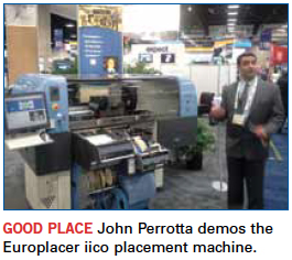
Placement
Universal’s Fuzion was likely the most talked-about new placement platform. It features two head types with overlapping component capability, meaning engineers won’t need to change out the heads. It supports up to 144 feeders, which is a big jump in capacity, and reportedly has a changeover time of 15 to 20 minutes. The IPC-9850 rate is up to 30,000 cph, and the component range is 01005 to 150 x 150mm, depending on which machine is used. All in all, a very flexible new mounter has arrived.
Panasonic also had an interesting development with the AM100, a single head (single beam) mounter capable of placing components ranging from 0402mm to 120 x 90 x 28mm, large connectors, odd-shaped parts, and advanced packaging types such as PoP. It also featured non-stop changeover, allowing the next product to be prepped while production is running.
Hitachi’s Sigma F8 was another machine that is forcing a lot of functionality (four 15-nozzle heads) into a smallish (1,280 x 2,240mm) footprint.
It wasn’t all just surface mount. Panasonic debuted the AV123 axial inserter, which features 30,000 cph performance on a small (there’s that word again) platform.
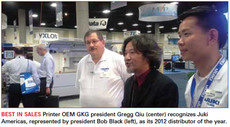
Juki’s Bob Black indicated a new JM series would be out in June. Juki also happily accepted GKG’s 2012 Distributor of the Year award.
Siplace and Panasonic joined Universal as placement companies indicating growth in 2012.
Soldering/Materials
ECD has a new sensor-based system that aggregates humidity data from up to 25 points in the factory and consolidates it in a mobile app. FCT Assembly discussed NanoSlic, a cylane molecule-based nanocoated stencil said to retain the coating longer than phosphorus-based versions. (Expect to see more cylane-based flavors as the second-generation nanocoats appear.) It’s due for release in June. Count DEK among those that expect to see more coatings introduced, reporting “great results” by customers.
BTU’s Dynamo could be a game changer. (We say “could,” because the machine won’t be shown until April.) It’s a new convection reflow platform with 8, 10 or 12 zones, capable of running air or nitrogen, but with 20 to 25% less energy use than its Pyramax cousin. BTU cut the energy by reducing the number of blower motors in the heater section, instead placing one outside the chamber where it can handle two zones at once.
Finetech showed a slick tool for reworking package-on-package and QFNs.
It’s been awhile since solder material companies used a trade show to roll out new products. Instead, they leverage the events to formally announce products that were developed for specific applications or customers, in some cases, months or years earlier. Apex was the first show we saw Enthone and Alpha under their new corporate banner, Alent. There was one revelation, however: Henkel is rebranding its surface mount materials under the Loctite name.
Finally, the IPC-A-610 meeting drew 74 attendees, a big number even for the IPC’s largest task group. Of some concern, it appears the solder types have been removed from the latest J-STD-006, rendering the document as a listing of solder alloys, but not much more.
Test/Inspection
As users grapple with smaller products and tighter test access, the test strategy is inherently changing. Boundary scan is becoming more prevalent, as is BIST for chip-to-chip communication.
CyberOptics, ASC (AP500, a fully automatic benchtop 3D SPI), and Newly (n=1 first-article inspection, plus board resistance and capacitance checks) were among those pushing smaller footprints.
Koh Young has a deal with KIC to jointly develop a tracking system to report profile and joint data, which then will be displayed in Koh Young’s pre- and post-reflow results.
Mirtec’s switch to CoaxPress cameras boosted the speed of its MV-9 series, which includes all LED and 2D/3D AOI, to 25 GB/sec., up from 5 GB/sec.
Nordson Dage has a new, undisclosed platform due out at Nepcon China.
Fabrication
We wish there was more to discuss on the fab side. As noted in past years, the Asian-based trade shows (JPCA, CPCA, HKPCA) are the top sites for developments in printed circuit board fabrication. There were, however, a couple of developments that caught our eye.
Remember the ESI mechanical drill team? They are regrouping at Interdyne, and the early results are impressive. Consider a granite base, six-head mechanical drill with a so-called laminated “wing” that moves in the Y axis while the spindles move in the X. The linear motors are tied directly to the 250km spindles. The new drill uses standard bits and reportedly is capable of 2 mil holes at a rate of 1000 hits/min., and can drill a 441 mil backpanel with 90 mil thick copper at 110 hits/min. When did the last new drill technology come out?
Also, Rainbow Technology discussed its automated vertical develop/etch/strip line, which runs on 4kW of power, has full automatic handling, and requires no solvents. The throughput is 90 panels/hr., and beta testing begins this year.
As always, the show is too large to detail every new development here. For the full list of new assembly products and materials, go to http://www.circuitsassembly.com/cms/ipc2013.
For fabrication-related products and materials, go to http://www.pcdandf.com/cms/ipc2013.
While Apex likely remains second to Productronica as a site for assembly equipment launches (its fabrication-based Expo half has long since ceded that designation), we did note more than a few exhibitors reporting they were holding launches until Nepcon China in late April. Outliers or the start of a trend? It’s something to watch.

High Hopes for 2013 NPI Winners
The annual Apex trade show represents the honorary start to the new year. It’s also an end of sorts: the culmination of the rookie year for products introduced at the previous Apex.
Each year at Apex, PCD&F and CIRCUITS ASSEMBLY announce winners of the New Product Introduction Awards. The NPI Awards recognizes leading new products during the past 12 months. An independent panel of practicing industry engineers selects the recipients.
This year’s electronics assembly equipment, materials and software winners are Microscan (Mini Hawk Xi); Speedprint (SP710avi); Count On Tools (ezLOAD PCB Support System); Austin American Technology (NanoJet Aqueous Inline Cleaner); BPM Microsystems (2800ISP In-System Device Programmer); Nordson Asymtek (NexJet); Mirtec (MV-9 2D/3D In-Line AOI Series); Acculogic (Ultimate Accuracy Package for Flying Scorpion); Multitest (InStrip 3D); VJ Electronix (Vertex II X-Ray Inspection System); Parmi (SPI HS70); Nihon Superior (SN100C P604 D4 Solder Paste); Count On Tools (Stripfeeder .mod Series); Universal Instruments (FuzionXC2-37); Rehm Thermal Systems (Vision XP 934 Quad Lane Convection Reflow Oven); ACE Production Technologies (KISS-205 Selective Soldering); Kyzen (Aquanox A4639 Aqueous Solution); Cogiscan (TTC Middleware); Viscom (SPI-AOI Uplink); EVS International (EVS 10K Solder Recovery); FCT Assembly (NanoCoat Multilayer System); Air Vac Engineering (PCBRM100); AIM (NC277 Liquid Flux), and CGI Americas (Newly n=1 First Article Inspection System).
The winners of the PCD&F NPI Awards for PCB fabrication are Nordson March (FlexVIA Plasma System); Rogers (RO4835 Laminate), and Dow Electronic Materials (Microfill THF-100 Electrolytic Copper).
“Each year there’s a few true, exciting innovations,” said Mike Buetow, editor in chief of PCD&F and Circuits Assembly. “We are thrilled to recognize
these companies for their efforts.”
Mack, ESI, Naprotek 2013 SEA Big Winners
CIRCUITS ASSEMBLY on Feb. 19 announced the winners of its 2013 Service Excellence Awards for EMS providers and electronics assembly equipment, materials and software suppliers. Circuits Assembly recognized companies that received the highest customer service ratings, as judged by their own customers, during a ceremony at the IPC Apex Expo trade show.
In the EMS category, the overall winners were Mack Technologies (sales of $101 million to $500 million), Electronic Systems Inc. (sales of $20 million to $100 million), and Naprotek (sales under $20 million).
The EMS companies with the highest scores in each of five individual service categories also received awards. (Overall winners were excluded from winning individual categories.) In the small-company category, ACD, Spectrum Assembly, and NexLogic Technologies tied for dependability. ACD also won for quality, and tied Pride Industries, Spectrum Assembly, and BESTProto for responsiveness. BESTProto and ACD tied for technology, while Pride Industries took home the award for value.
For firms with revenue between $20 million and $100 million, Western Electronics took top honors for dependability and responsiveness. Applied Technical Services tied Sparton Electronics for value. Western Electronics and Applied Technical Services shared the top spots for quality and technology.
For EMS companies with revenue between $101 million and $500 million, EPIC Technologies swept all five individual categories.
Electronics assembly equipment award winners were Assembléon for pick-and-place; Speedprint Technology for screen printing; Kyzen for cleaning/processing materials; Mirtec for test and inspection; Nordson EFD for materials; Nordson Asymtek for dispensing, and KIC for soldering equipment. Customers of SEA participants rated each company on a scale of 1 (poor) to 5 (superior) in five service categories. – CD
Mike Buetow is editor in chief of PCD&F and CIRCUITS ASSEMBLY; mbuetow@upmediagroup.com.
Tooling design and validation makes the difference.
Robotics has been gaining visibility the past few years in everything from media reports to commercials. Robotics serves many different industry sectors to assist in everyday life, from our homes to medical facilities, manufacturing plants and even the military. Behind every robot is the manufacturing assembly process of how the robot was built. Here, the author details some key areas of the Benchmark Electronics New Hampshire division Robotics manufacturing process, from a prototype or new-build stage to steady-state production. Working with our local customer’s design team, Benchmark specializes in complex electromechanical assembly work. In the past five years, a total of six robotics programs ranging in size from a throwable unit to an eleven-foot-tall giant have been assembled. The programs manufactured serve the full range of applications above, and include a design build-stage to steady-state production phases.
Supply-chain involvement. Early involvement and communication with the supply chain becomes very important to understand supplier capability and design for manufacturing (DfM) issues that may arise. No matter what stage the supplier may be on the chain, this early involvement gets the supplier engaged in the design phase and pre-production ramp to volume.
Early supplier involvement gives time to develop tooling, work out process issues and “Lean” and streamline the manufacturing process. This partnership with the supplier also builds a product knowledge base if a DfM issue occurs with integration or, in the event of engineering change orders, when quickturn results are needed for proving the new design.
Skilled workforce. With any manufacturing workforce, skill and experience to perform the task are important. Robotics assembly requires specific talents and skills given its complex electromechanical assemblies. Attention to detail, mechanical skills, feedback and continuous improvement orientation are some of the key attributes of the workforce.
Required skills may be different during the prototype or design phase in comparison to the production stage or steady-state product build. During the first build or prototype, the assembly learning curve and design for manufacturing concerns are steep. With any new design, this includes determining if the assembly goes together correctly, identifying modification needed, and reacting to changes along the way such as design updates, ECOs and other assembly roadblocks.
During the production stage, different skills may be required, given that the assembly process is steady-state and production-ready, with detailed work instructions completed to provide visual aid to the assembly operator. At this point, the ability to focus on quality, efficiency and incremental process improvement becomes more critical.
Tooling design and turnaround. During any complex electromechanical assembly introduction, designing and developing tooling assists the operation in manufacturability. Tooling designed and developed during the initial build stage requires a quick turnaround, given the need to test and evaluate the final product, and time-to-market requirements. Tooling can be designed and machined by a drawing or using a picture of the actual product. In some cases, the final part will be required to validate the tooling. Modifications may be required to change the specific tool, depending on fit checks or functionality.
When the complex mechanical assembly has been transitioned to production, additional production tooling may be helpful to reduce assembly cycle time or assist the mechanical assembler for ease of manufacturing. Additional tooling may also be helpful to poka-yoke or mistake-proof an operation. This may be helpful during an inspection or validation of product stage.
Figure 1 is a tool used in the mechanical assembly operation. The tool is a mistake-proofing tool used to verify product is built correctly. The product is a motor that is built in two different configurations (left and right) that has an opportunity to be assembled incorrectly given similar base part numbers. Use of the tool shown in Figure 1 quickly verifies that the motor has been assembled for the correct side.

With any tooling developed, a validation will be required. The validation of the tooling will confirm that the tool is not causing defects or other issues that may impact form, fit or function at a next-level assembly operation. The key is to validate the tooling on one piece of product to prove out the design concept. A tooling validation checklist may be helpful to assist in this operation to detail the key steps of the assembly process and points for inspection. A few key points of validation are:
- Verification of product in next-level assembly operation to ensure the tool did not affect form, fit or function. (Example: Damage to a screw hole.)
- Inspection of product to ensure no damage occurred, and the product meets inspection criteria. It is important to sample several assemblies, to develop confidence in the tool’s ability to work within normal range of variation.
- Inspect the tool regularly, on a schedule, to make sure no damage occurs.
Prototype to production. During the prototype stage, the main goal is to develop and prove out tooling, work instructions or visual aids and to work out any DfM issues. During this production readiness, a baseline should be known of how many production units will be required, thus determining assembly space, flow, equipment and tooling needed to meet customer demand. Opportunities will exist to implement Lean manufacturing principles such as point-of-use material storage or assembly pass along line. Cycle time may be reduced by implementing additional tooling or modification to tooling that will assemble a piece part faster: for example, press-fit tooling that can do multiple pieces at the same time or electric drivers for mechanical assemblies with many screw locations at an operation.
Robotics assembly requires many skills and talents from all involved within the manufacturing assembly process and team. From supply-chain communication, to quickturn manufacturing tooling design, to streamlining an assembly process for steady state production volume, all is required for a successful robotics assembly process from prototype to production.

Scott Mazur is a manufacturing staff engineer supporting various robotics assemblies and programs at Benchmark Electronics New Hampshire Division (benchmark.com); scott.mazur@bench.com.

Press Releases
- Aven Welcomes Max Ramos to Strengthen Distribution Partner Operations
- ubersmt Expands SMT Line with Juki G-Titan Printer and RS-1R Placement System
- Keiron Technologies to Host LiFT Webinar Focusing on Solving Solder Paste Printing Challenges
- Express Manufacturing, Inc. Strengthens Test Capability with Acculogic Flying Probe System