

MassChallenge, a not-for-profit accelerator program, aims to “create a bigger pie” by helping innovators get to market.
In a 27,000 sq. ft. office on the 14th floor of a Boston Harbor high rise, scores of innovators in residence toil away, trying to make their dreams reality. Four quadrants of cubicles form the basic layout, abutted by casual open meeting areas, a compact soundproof recording studio, and a galley kitchen. The walls are covered in encouraging aphorisms such as “What it takes” and “Take it until you make it.”
On an otherwise quiet Friday morning in October, a handful of residents listened intently to a series of talks on finding revenue sources. Among them was a team of advisors to the Mayor of London, dispatched to get a handle on the program in hopes of launching their own.
The program, in this case, is MassChallenge, a global accelerator program built around an annual competition whereby startups are graded, winnowed, trained and ultimately compete for no-strings-attached funding.
Now entering its fifth year, MassChallenge is embarking on a new expansion platform, even as it aids hundreds of small firms trying to beat the odds and make a difference in the software and hardware fields. It’s a startup for startups.
A ‘wacky’ model. MassChallenge is considered to be an accelerator, which is characterized by a short-term training program – up to four months – after which the entrepreneurs are back on their own. An incubator, on the other hand, takes the entrepreneur’s idea and matches it with professional managers. The latter also takes a bigger share of the startup’s equity.
In terms of its structure, MassChallenge is noticeably different from its peers. Most accelerators are run by investors, groups that expect a hefty return. MassChallenge focuses instead on innovator success. “Our model is a little wacky,” concedes director of marketing Robby Bitting, noting that under the firm’s framework, participants are essentially competing for grants.
Applications are soaring. In 2010, the first year of the Challenge, some 446 entrepreneurs applied. That number nearly doubled to 733 in 2011, and then nearly doubled again to 1237 in 2012. The current class of applicants was made up of nearly 1,200 companies from 44 countries.
From the initial submissions, a group of more than 300 judges with expertise in a broad range of disciplines pares the list to 128. Those lucky few take up residence at the MassChallenge headquarters in the so-called Innovation District on Fan Pier in South Boston. Their exclusive perch allows the inventors panoramic views of the Boston Harbor skyline, including regular flights landing at Logan Airport, just across the inlet to the bay.
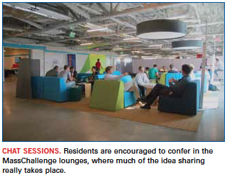
Inside, the site has the character and spontaneity of any of a thousand Silicon Valley startups. Game tables, colorful oversized furniture and scores of cubicles reinforce the notion that innovation breeds innovation. Participants are encouraged, through the office layout and the accelerator’s instructional and social programs, to mingle and share ideas. And share they do, despite the fact that each company is competing for a share of roughly $1.5 million in cash prizes. But therein lies the magic: The founders believe the “greed is good” thinking spawned by many a Wall Street guru is fallacy, and MassChallenge is their response.
Creating a bigger pie. MassChallenge is the brainchild of John Harthorne and Akhil Nigam, a pair of former Bain Consulting whiz kids who grew disenchanted with the relentless emphasis on profits over true and potentially radical change. Both were itching to create startups and create value. Then the market crashed. “Money for entrepreneurs dried up,” noted Bitting. “So much of this had to do with greed. People wanted a bigger slice of the pie without creating a bigger pie.”
Says Harthorne: “For 30 years, business schools have force-fed this idea that profit is what matters. We’ve seen with the recent recession that that model doesn’t work. You build a company because you want to do something for the customers. Only once you’ve (captured) their love can you then extract a profit.
“There are a lot of short-sighted strategies with a disregard for rational thought. By focusing on profit, you diminish it. By solving problems, you create a new value that doesn’t exist.”
The pair founded MassChallenge in 2010 in hopes of spurring an innovation renaissance. “Making a profit is not the issue. It’s getting the innovators to collaborate and push each other higher,” Harthorne says.
MassChallenge does this through somewhat traditional accelerator means, offering weekly classes on marketing, sales, building an organization and attracting funding, taught by a host of international stars in their respective disciplines. Funding comes from blue chip companies inside and outside the tech field, such as Microsoft, IBM, Fidelity, American Airlines, and various academic institutions, among others. Innovators are paired with mentors, at an average ratio (MassChallenge seemingly measures everything) of 3.6 mentors per startup.
Residents, like those on that October morning, experience an extensive curriculum that covers everything from leadership to team building, finance and pitch practice, brand building, marketing to the public, and media. MassChallenge attempts to help residents achieve in four months what would typically take a year or more. The mentors help oversee deadlines and progress.
It sounds like a hyper-compressed MBA, but that’s not the idea, the founders say. Rather, MassChallenge program is intended as a launching pad. Finalists, they say, want the access to the experts. “They want too many opportunities, not too few,” stresses Bitting.
Major impact. What also sets MassChallenge apart is its fee structure. For starters, it’s a not-for-profit organization. Entrepreneurs pay just $200 to apply. Unlike other accelerator programs, the focus is on impact, not revenue generation. “Impact,” the founders admit, is a nebulous term, and intentionally so. “We like companies that are solving a very technical problem. It also allows us to take on social enterprises that are also nonprofits,” Bitting says. Indeed, MassChallenge takes no equity in or places other restrictions on its residents.
Judging is handled by industry experts, with four to six judges per application. The first step is a review of all the online submissions, which takes place each April. The pool is then reduced to about 350 companies. The next phase involves pitching the idea in front of the judges, who assess the impact of the applicant’s idea. That impact could be very different, based on the industry the end-product is designed for. In one instance, it might be a cure for a disease. Or it could provide a method for bringing education to people who need it. Perhaps it is a technical solution (see sidebar). More conventionally, it could have the potential for a high growth business that would create a lot of jobs.
Judges evaluate each idea on its potential impact and the ability to achieve that impact, or in their parlance, “traction and feasibility.” They look at the business model, the customer acquisition strategy, the founders and their team (most of which are very small), the potential for patents (as well as competing ones), and the competitive landscape. The face-to-face presentation takes 20 minutes, after which the judges cut the applicant pool to 128.
Then the fun begins. The pool takes up residence at the MassChallenge headquarters. There, they will spend the next four months splitting time between polishing their concepts and the crash course in finance and marketing. Come September, the residents will pitch their ideas again, at which point the judges will determine which 26 are eligible for cash grants of up to $100,000. (Herein is another difference between MassChallenge and other accelerators, most of which award seed money at the beginning of the program, not the end.) At the beginning of October, the lucky 26 will make their last pitch, and judges provide written feedback and single out 12 companies for $50,000 awards and four finalists for $100,000 grants.
The open floor plan and mixing of disciplines and industries goes a long way toward igniting the innovative spirit, the founders say. On a given day, there might be 300 people working in the MassChallenge office. “A mobile company has no business meeting with a biotech firm, except there’s a certain level of comfort seeing someone sitting by you and achieving. It’s why people work out in groups. We want them to see each other. They make a sale and go ‘high five’ each other,” Bitting says.
In theory, the rapid experimentation also permits companies to fail quickly and move on to the next step. In truth, many are growing. To date, 89% of the 489 companies accepted to the program remain active.
Recycling knowledge. The mentor program is a mix of inbound and outbound experts. Sponsors provide both talent and legal advice. Also, there’s a pay-it-back aspect, as some of the finalists act as mentors for future classes. Many enter the mentor program and offer advice on both the technical program and the side issues, such as dealing with investors, the organization says.
Many of the inventors remain in the Boston area even after their apprenticeship is over. Even those international participants who return abroad tend to maintain their new local connections. The obvious question then is, Could an AustinChallenge or SanJoseChallenge be far off? In fact, there is interest in London to develop a similar program (the discussions involve locating the program in a formal royal palace), and MassChallenge Israel is in the works. Other places being actively explored in the US include Houston, Denver, North Carolina, Washington, DC, and ultimately California, while overseas interest has been focused on Switzerland, Berlin, Russia and Columbia. MassChallenge isn’t worried about cannibalizing the existing program because two-thirds of the current finalists come from Massachusetts.
The vision Harthorne lays out for MassChallenge is audacious: to restore the credibility to the soul of America and the world. “There’s this deep sense we lost our way. There’s too much emphasis on profits. We’ve become perverted about it. It’s not a good way of building sustainable systems. It’s incredibly counterproductive. The reading on the Statue of Liberty isn’t, ‘Give me your profits and money.’ ”
What Harthorne isn’t is some Harvard MBA with a few years of finance under his belt who now dispenses conventional wisdom like John D. Rockefeller gave away dimes to Depression-era children. (Although in fact, he is a graduate of MIT’s Sloan School of Management.) Harthorne puts to use his own experience in starting up MassChallenge to share with teams that enter the accelerator. “The first year of MassChallenge,” he notes, “we were an earlier stage startup than 60% of the companies we worked with.”
Those who have successfully reached the finals speak highly of their experience. Molly Farison is a senior in electrical engineering whose company, Lilypad Scales, created an easy-to-use scale that helps wheelchair users track their weight on their own, in their home. The scale resembles a thin 4 x 4' rug and comes with a remote control-like reader. “You can’t just sell your product in an online store,” notes Farison, who calls her time in residence “a quick and dirty practical MBA. Finding the best distributors for your product and getting them to sell it is the key to scaling.”
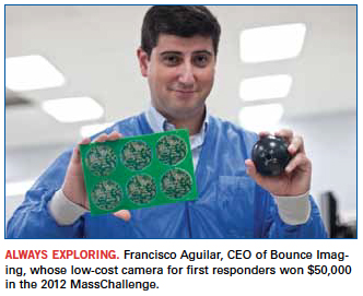
For Francisco Aguilar, CEO of Bounce Imaging (see sidebar), MassChallenge was invaluable for finding everything from engineers to legal help to access to software programs such as SolidWorks, which otherwise would have been expensive to license. The cofounders “know everyone in the world and want to connect you,” he says. And while those with experience in electronics like himself may know how to design a product, the mentors at MassChallenge have the background in finance and investing, customer segregation and publicity to get a company off the ground. Bounce has received accolades from Popular Science, and the Explorer was named one of Time Magazine’s Best Inventions of 2012.
“MassChallenge has been essential to our success and traction,” Aguilar says. “We could have been working on this for years.”
MassChallenge is open to any early-stage entrepreneurs, be they in software or hardware. What all teams must have, Harthorne says, is a good plan, the willingness to work their butts off, and to be lucky. The competition helps, too. “You can genuinely hurt a startup by being too easy on them.”
Electronics engineers take note: MassChallenge is in the business of helping startups, not hurting them. We may take our iPhones and Bose speakers for granted today, but every company started with an inventor and an idea. MassChallenge has created a pathway for the next Steve Jobs or Amar Bose to turn their vision for a better tomorrow into reality. That’s an exciting path to be on.
Exciting Times
“Our industry has gotten (expletive) boring. We need to make it exciting.” So says Rich Breault, president of Lightspeed Manufacturing, the CIRCUITS ASSEMBLY EMS Company of the Year.
Breault’s frankness belies the serene landscape inside One Marina Park Drive, where engineers and innovators are quietly plugging away at their cubes. A few take up a game of Ping Pong, while others mill in small groups of two or three, comparing notes like college students in a library, which some still are, it should be noted.
Breault began teaming with MassChallenge two years ago. In 2012, Lightspeed put a small lab inside the Boston accelerator’s headquarters. The EMS firm provides onsite assembly help, aided by a collection of software (Solidworks and AutoCAD) and hardware tools (soldering irons, a Sciencescope meter, and a Formlabs 3D printer). When MassChallenge relocates next year to another site nearby, Breault plans to expand his operation to include a full SMT line, including a pair of Quad placement machines building prototypes, a drill press and belt sander for mockups, and a full-time staffer to run the Lightspeed “Answer Desk.”
Lightspeed’s involvement has led the EMS firm to Bounce Imaging, on whose board Breault now sits. Struck and dismayed by the aftermath of the Haiti earthquake in 2010, when responders could not get quickly to the hundreds of thousands of victims, Bounce founder Francisco Aguilar conceived a low-cost camera for first responders that can be used without special training. Aided by Breault’s manufacturing help, the company’s device, named Explorer, won $50,000 in the 2012 MassChallenge.
With the Explorer, Aguilar sees a huge potential market for police and firefighters who on a daily basis experience the same basic problems, if to a different degree. And since then, Lightspeed has picked up three additional customers via the MassChallenge.
Mike Buetow is editor in chief of PCD&F/Circuits Assembly; mbuetow@upmediagroup.com.
Ed.: For a related article on Lightspeed, click here.
The five-year forecast calls for 38% growth, driven by the industrial and communications sectors.
The electronics manufacturing market is big; global assembly of printed circuit boards exceeded $1 trillion last year. Given such a vast marketplace, there are numerous opportunities for companies to specialize in one or another technology. Embedded computing is one such technology with a great deal of promise.
The merchant embedded computing (MEC) market is a specialized market within electronics assembly. It is a dynamic industry, with advances occurring continuously, thanks to an energetic standards development effort. MEC modules and components are board-level computing systems and solutions, based on specifications controlled by a dozen or so standards organizations that have grown up along with the industry. Literally hundreds of standards – adopted or still under development – are controlling the design and manufacture of embedded applications. Also, more than 200 companies worldwide are developing and manufacturing products, with an additional 100 to 200 participating in the distribution and assembly of embedded computing boards and their components.
New Venture Research has been tracking the merchant embedding computing market for over 15 years. In our latest report, the Merchant Embedded Computing Market – 2013 Edition, we provide a historical analysis and forecasts of the embedded computing market, as well as our observations of market trends for the coming five years. Data are based on field-user surveys and interviews by industry participants, as well as our other reports related to electronics assembly. We analyze the overall market from three separate, but interrelated, perspectives:
- Applications: five application segments targeted by MEC companies.
- Bus architectures: nine categories, based on the bus architecture and form factors of embedded boards and modules.
- Board function: four functional design categories of board-level products.
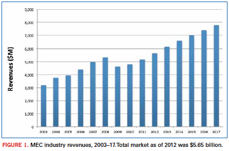
Sadly, any current analysis of today’s electronics marketplace must start with the recession of 2009 – a near-economic calamity often compared to the Great Depression of the 1930s. The recession left an indelible mark on virtually every aspect of the global economy, not least the electronics assembly markets, including the market for embedded computing. Figure 1 shows the impact of the economic downturn on the MEC industry. In 2009, there was an abrupt and significant reversal in the growth rate, as well as total revenues of the MEC market. The pain was felt in virtually every segment of the MEC market. Yet, seen from a wider perspective, the “Great Recession” was little more than a blip in a history of consistent growth by the industry. Despite the severity of the downturn, by 2012 the market had fully recovered in terms of total market size, and seemingly in momentum. Moreover, the MEC market is projected to continue growing well into the future, according to our research.
One reason for our optimism is based on the nature of the MEC industry. Thanks to the evolution of old standards into new, and more advanced ones, the manufacturers of embedded computing modules and components are constantly working at the leading-edge of technology, providing products that ultimately save customers money. Ivan Straznicky, a technical fellow at Curtiss-Wright Controls Defense Systems, a long-time player in the merchant embedded computing market, points out that today’s merchant vendors can take advantage of the opportunity of “relieving the pain of our customers.” According to Straznicky, “Whereas in the past, they would have been tempted to build these components themselves, they now come to us because we have ready-made solutions that have been developed across multiple customers and been field-proven.” This is both the benefit and the promise of embedded computing.
Positive trends. A number of market trends point toward a growing MEC market, including:
- Purchasing by large sectors of the economy has picked up for MEC products, as telecommunications companies, industrial automation companies and government (particularly in the defense industry) are spending on repairing and replacing equipment that depend on embedded computing devices. Such maintenance work all but stopped during the recession, so pent-up demand is helping drive the market.
- The transition toward digital communications, as well as skyrocketing traffic, is driving telecommunications carriers to rapidly upgrade their networks and private enterprise to increasingly move toward IP and data communications products. The MEC industry is well placed to take advantage of this transition.
- Next-generation, high-integration silicon is enabling manufacturers to design board-level systems with capabilities not possible even five or six years ago. Improvements include lower energy consumption and very high-speed serial bus interconnects, all within small form factors. Embedded computing vendors are tightly focused on leading-edge technologies and board architectures, which will place them at the forefront of emerging markets in the coming years.
Microprocessor manufacturers, particularly Intel, continue to raise the bar with ever greater integration and more powerful chips, and as Jim Renehan, director of marketing at Gainesville, GA-based Trenton Systems points out, there is a need among standards to move up the “food-chain” to provide more capability for boards and plug-in cards.
MEC vendors face competition from other electronics sectors, as well, including the electronics manufacturing services industry. (NVR tracks the EMS market in a companion report, The Worldwide Electronics Manufacturing Services Market.) Both industries depend on sales to OEMs and to government prime contractors. EMS vendors have an advantage in selling products in large numbers at low cost. Many MEC vendors, on the other hand, are small and specialized in niche markets. Their products are, by nature, customized and sold in small quantities. But the rewards in such a business model can be high, as the vendors can act quickly and build to specifications not possible by EMS competitors.
Some segments of the MEC industry have fared better than others as the market has emerged from the downturn, and in the following sections, we analyze the issues and opportunities for each of the major market sectors covered by our report.
Application markets. The MEC market consists of four leading application markets – communications, industrial automation, medical, and military/aerospace – and an “other” category that includes a number of vertical markets, such as transportation, security, surveillance, point-of-sale/kiosk applications, etc.
These application markets tend to have very specific product requirements that differentiate them from one another, as well as from other electronics assembly market segments such as PCs and the general purpose embedded electronics markets. Requirements include operating in harsh environmental conditions of temperature, humidity or vibration; greater reliability and security; and specific real-time computing functionality. Hence, the market leaders, competitive forces, growth rates and size of the different application segments vary widely.
Figure 2 presents a top-level analysis of the MEC market from the point of view of the five application market segments for 2012. Prior to the industry downturn, the communications application market was the largest single market segment. However, general industrial automation applications have made a stronger comeback than has been seen in the telecommunications sector and, by 2012, had become the largest and fastest growing MEC market.
The growth of the industrial automation application market – “Big Data,” as Renehan refers to it – is at least partially a function of corporations around the world upgrading their circa-2007 systems with new energy-efficient systems. It is claimed that these new technologies can enable users to replace 10 servers with one new multicore server and permit an energy payback in fewer than 18 months. Other advances include large increases in the ability to move massive amounts of data in and out of systems, requiring interconnect speeds to grow from 1Gbps today to 10 and 40Gbps. This is good news for MEC communication suppliers, as well as industrial manufacturers.
Over the next five years, we expect this trend to continue. While the communications application market will grow at a pace equal with the overall market, industrial automation products will outpace communications, and will account for more than one-third of the total market by 2017.
Medical applications was also hit hard by the financial crisis, which slowed MEC-based purchases of large equipment considerably. Unlike other manufacturing sectors, which have begun to replace and upgrade equipment, new spending in the medical segment is still depressed, in part due to uncertainty in the US about forthcoming changes in the national healthcare system. Consequently, we do not expect this market to grow as quickly as other segments.
Military and aerospace applications suffered in much the same way as industrial automation. And it has rebounded for much the same reason. NVR expects that various challenges of providing to the mil/aero market will slow its growth rate, somewhat. Growth in this market is closely tied to politics and to the security issues facing all defense-related markets, and these challenges will impact short-term growth rates.
Even so, Michael Macpherson, vice president of strategic planning at Curtiss-Wright, points out that, overall, the global picture for this market segment looks quite healthy. Curtiss-Wright is a leading competitor in the military and aerospace market segment. From Macpherson’s point of view, the market constraints have been primarily in the US. He specifically points to the debates over the budget and sequestration as having put pressure on the “topline of the defense market.” As a consequence, there may not be quite as many of the multi-billion-dollar programs. “But we do the electronics,” Macpherson notes. “And while there may not be as many new, big programs, the fact that they are still upgrading and doing service life extension for existing platforms means they are still upgrading the electronics, and that is good for us.”
Rodger Hosking, a vice president and cofounder of Pentek, a New Jersey-based merchant embedded computing vendor that also focuses on government and military markets, agrees. One of the drivers of this market, he points out, is that government organizations are faced with maintenance costs of older systems that can be replaced by newer systems with “one tenth of the cost, one tenth the power dissipation and one hundred times the performance. So, you look at the economics, as well as the strategic advantages of some new technology, and it’s quite a simple equation for a government electronics customer to justify upgrading or replacing older equipment.”
Bus architecture markets. Market penetration by the various embedded computing bus architectures is driven as much by technology as it is by market forces. The nine bus architecture categories defined in our report are as follows:
- PCI.
- CompactPCI.
- AdvancedTCA (ATCA).
- VMEbus.
- PMC.
- AdvancedMC (AMC) and MicroTCA.
- PC/104 and its variants, plus EPIC, EBX and motherboards (ATX and ITX).
- COM and COM Express.
- Other.
Each MEC bus architecture has a different rate of adoption depending on the needs of individual application segments. Some are older parallel-bus technologies and nearing their end-of-life, as is the case for PCI-based buses, specifically the PCI and CompactPCI architectures. CompactPCI (cPCI) has historically captured the largest share of the MEC market, but this is changing, as PCI architecture market shares are rapidly shrinking. Figure 3 shows that cPCI was the largest single bus architecture segment in 2012. NVR expects that within two years, its market share will drop below that of VMEbus – however, not necessarily owing to any great growth by the latter segment. Also, an “old” bus architecture, VMEbus standards and products have changed and adapted to the advances in technology and consequently will remain a significant product segment. Helping VMEbus products stay competitive is the fact that this architecture is specifically designed for extreme environments, a design feature that makes this an ideal product for many industrial automation applications, especially for mil/aero applications.
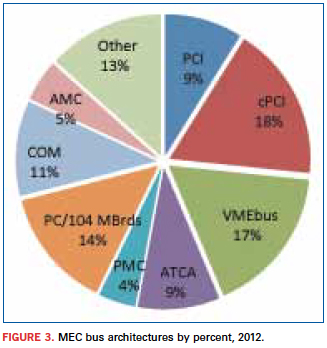
Yet, VMEbus will grow only more or less equally to the overall market, while the big winners for the future are products driving the industry toward higher integration in smaller form factors. This trend is reflected in the growth rates of the computer-on-module (COM) bus architecture. This technology will grow at double-digit rates between 2012 and 2017, largely because it is enabling vendors to create complete systems on a highly integrated single board. PC/104 and its variants are also small form factor architectures, but are not as trendy as COM.
Looking to the future, though, if you had to describe the most significant trend in the evolution of MEC architectures, it can be pared down to a single word: “Faster,” says Todd Wynia, VP of planning and development at Emerson Network Power Embedded Computing. “The industry has shifted from bus-based architectures to a fabric-based industry,” he says. “Instead of being the VMEbus or compactPCI of the past, it’s now Ethernet-based backplanes for architectures like ATCA or the evolution of compactPCI or VPX – all fabric-based interfaces. And the evolution of those interfaces is ever-faster.”
In keeping with that evolution, we expect to see a rapid expansion of AdvancedTCA, as well as AdvancedMC bus architectures. Both of these form factors were originally developed for telecommunications, but they have since expanded into industrial automation markets and are consequently experiencing high growth rates. AdvancedMC is particularly worth watching. The AMC specification was only adopted in 2005, yet we expect that it will capture nearly 8% of the total MEC market by 2017.
New bus structures are continuously being developed by merchant vendors. Basing their design and manufacturing on existing standards and on new specifications being developed by the standards organizations, the vendors sell a bewildering array of off-the-shelf embedded board designs to OEMs and even end-users. Moreover, most companies are willing to develop custom architectures based on existing product lines. This constant innovation serves to strengthen the MEC industry and at the same time fend off competition from EMS vendors. High volume is not necessarily the name of this game; rather it is innovation, customization and optimization that will drive the MEC market through the next decade.
Board function markets. The MEC industry can also be categorized according to the functional design of embedded boards. NVR identifies four board function categories: single-board computers (SBCs), digital signal processor boards (DSPs), I/O boards, and other board functions. The last category incorporates a huge number of diverse and specific functions, many of which are custom designs, including switchboards, chassis, backplanes, and system integration devices. The MEC board function markets are presented in Figure 4, providing market share of each functional category for 2012.
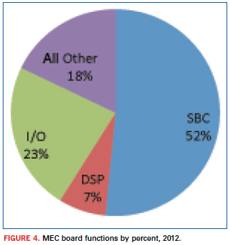
In some applications, I/O boards are proliferating and are customized to the wide spectrum of I/O functions that different applications use. Other board functions are also proliferating, mostly owing to a growing demand for custom products. But the real story for MEC board functions is a persistent shift toward single board computers. MEC vendors are more and more integrating all of the electronic components and functionality into SBCs, creating complete systems. (This trend goes hand in hand with the growth of COM bus architecture, which is, by definition, a SBC board function.) Leading manufacturers like GE Intelligent Platforms exemplify this trend. GE considers single board computers as increasingly significant for its product line. According to Ian McMurray, speaking for the embedded computing group, SBCs are at the heart of its military/aerospace business, incorporating an extensive range of component products, including microprocessors, sensor processing systems, video processing platforms, image processing technology and highly rugged routers and switches.
Increasing integration onto the SBC platform has always been a characteristic of this market segment, and it goes hand-in-hand with the evolution of bus architecture technology. The key elements driving this trend – processors, fabrics and integration – are leading increasingly toward advanced fabric-centric architectures, such as VPX, which McMurray notes has become the architecture of choice for new military programs at GE Intelligent Platforms. Moreover, as SBCs integrate and incorporate ever more of digital signal processing, graphics and I/O functionality, the need for separate DSPs and I/O boards decreases, and leads to growing demand for single board products like the COM Express form factor. Thus, already accounting for more than half the total MEC market in 2012, NVR projects that the SBC market segment will continue to expand its market share of the total MEC market over the next five years and beyond.
Conclusions
Throughout this discussion, we have touched only lightly on the thing that gives meaning to the merchant embedded computing market: the active, dynamic standards process. Despite a bewildering array of products and designs, the products that drive the MEC market are themselves driven by relatively few organizations that bring together (sometimes fierce) competitors to work collectively to develop open specifications that help everyone – manufacturers and customers alike. From the earliest consortia – such as VITA, PCI-SIG and PICMG – to the most recent – SFF-SIG and SGeT – these organizations empower manufacturers to concentrate, not on basic form factors and connectors, but on building the best mousetrap for the application.
Significant changes are happening in the MEC marketplace and in the electronics industry in general. Along with the evolution of technologies, such as the shift from parallel to serial and from simple buses to fabric-based architectures, the standards organizations are constantly evolving their standards to keep pace. As Moore’s Law continues to be demonstrated by ever more powerful chips, applications once needing discrete chips for separate tasks are being integrated into single, more densely packed chips, and new standards specifications will make it possible to integrate those chips into embedded designs. The challenges raised by decreasing size and increasing performance cannot effectively be addressed by individual companies. It is the PICMGs, VITAs and SFF-SIGs that will help speed these trends. It is these organizations that are helping define the future of embedded computing by advancing the technologies incorporated in standards specifications.
These trends are altering the MEC board market at an accelerated pace. Not only will much of today’s separate chip functionality get subsumed into a single chip design, but also the computational power and functionality of single-board computers will skyrocket. “There are always challenges to overcome,” concludes Rodger Hosking of Pentek. “That’s what keeps us in business, and it’s what keeps the industry going. The big driver is the silicon and component technology. Everything that we are surrounded by – the electronics in our cars, mobile electronics, everything – is getting more powerful, smaller, less expensive.”
Jerry Watkins is a senior analyst with New Venture Research and author of numerous syndicated reports in the telecommunications sector and more recently in the computing and merchant embedded computing industry; info@newventureresearch.com.
A 95% first-pass yield is the litmus test. Here’s how to get there.
Capital spending is an internal issue EMS providers constantly grapple with. At the back of the minds of the decision-makers are a host of related and nagging questions. Can we make do with existing equipment? What are our tradeoffs? Will we lose money using older assembly equipment? How will customers perceive older equipment? Can we satisfactorily deliver to OEMs with cutting-edge technologies?
Of all the associated capex questions, the most prominent should be: Do we provide the right levels of technology, manufacturing equipment and expertise to deliver the best product to the OEM?
One way to get there is through sophisticated automated optical inspection systems. The extraordinarily small component packaging and ever-shrinking PCB sizes require superior inspection solutions to detect assembly flaws and defects.
AOI is well-suited for checking tombstones, misaligned or missing components, wrong polarity, wrong parts, lifted leads, and lifted lead banks. AOI ensures that installed components are the right ones in terms of value and footprint. It also catches marginal opens, in which the assembled joint is minimal and certainly not 100%. In many cases, when the AOI operator manually presses on the joint in question, the connection is made.
When older AOI technology is used on the assembly floor, it often is in conjunction with testing, and the latter is expected to catch those latent defects that slip past AOI. A better process, however, is to upgrade the AOI machines. New features include advanced LED lighting, the color of that lighting, camera location, lens resolution, user interface, and better, more comprehensive algorithms for detecting components and flaws.
Beyond the equipment itself, the AOI operator or programmer plays an equally important role. AOI is designed to detect questionable components. However, it’s up to the operator to ensure defects are either “true” or “false.” One aspect they must be mindful of is defining the tolerance or pass code as tightly as possible for defining the right window for reading components on a PCB. Within this tweaking process, if the tolerance window is too tight, it can be increased. But if the region of interest is made too big, then the AOI passes virtually everything, and true faults will be missed.
The experienced AOI programmer will program the right part type, and accurately program the tolerance or pass code. In this second step, the operator performs program tweaking to train the AOI for the right component, as well as define the tolerances, the footprint, size of the rectangle, and the overall region of interest.
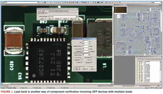
Figure 1 shows the lead bank indication on the AOI monitor. It is yet another way of component verification involving QFPs that have multiple leads. In this case, highly complex algorithms are put to use to inspect these particular components. These lead bank windows are larger in size to not only perform component verification, but also expedite the inspection process.
Compared to the earlier incandescent AOI lighting systems, LED technology has provided AOI operators superior brightness and a clearer, sharper focus on devices and hard-to-see board areas. Also, LED lighting spreads out the viewing area more uniformly to track down flaws and defects in the subject target or “region of interest.” Another advantage LEDs offer is the availability of different colors.
The color white is traditional. But LEDs allow the application of different color filters such as blue, red or an RGB (red, green, blue) option. These filters are especially valuable to improve visibility on small or overly shiny components.
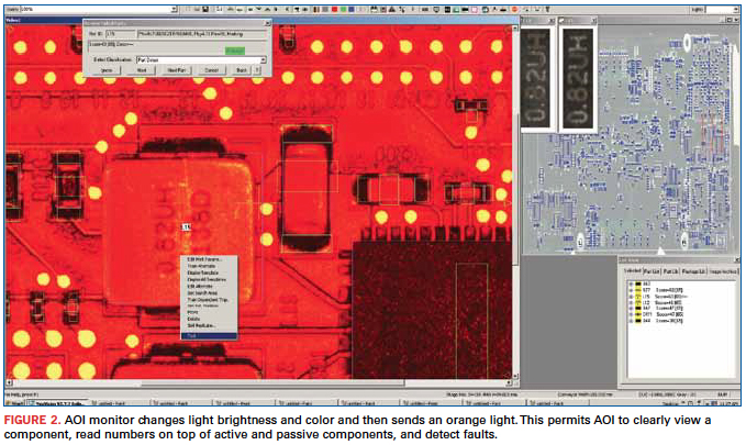
For example, a traditional white light immediately reflects off a glass-based package in the region of interest, creates a blank, and prevents the viewing of that component. Using advanced AOI features, the operator applies the different filters during programming or simply applies the different color lighting if already programmed. Figure 2 illustrates such a case where AOI changes light brightness and color and then sends an orange light. This permits the AOI to clearly view a component, read numbers on top of active and passive components, and detect faults.
As for camera locations, an effective AOI has five different viewing sites. One is on the left, another on the right, the third on the front, another on the back and one on top. This way, a board is captured from every angle. If component markings cannot be viewed from the top, the operator has the option of going to the side angle for a different view and the ability to detect that component. Having different cameras at different locations is a great help in determining and detecting true failures compared to false failures. A greater number of cameras offer better visibility on different sides and different angles with greater depth of field, giving greater coverage of the region of interest. Consequently, true and false faults are clearly seen with no visual ambiguities.
Newer AOI technologies have also introduced higher camera lens resolution. Today’s state-of-the-art AOI cameras sport 25MP. Five years ago, AOI featured 1MP cameras. The big jump in megapixels is providing considerable capability for component feature recognition and a much clearer view. These extra megapixels hand the operator a highly consistent and crisp picture of extremely small areas on top of components. These viewing advances come at a time when such passives as 0402, 0201 and now 01005 are so small that the human eye can barely see them. But with this large number of pixels, they can be clearly spotted.
Two other complementary features are zoom capability and depth of field. Particularly for extraordinarily small component packaging and tight PCB areas, the newer cameras can zoom in from 50 to 250X to closely view those shrinking board areas. Meanwhile, depth of field spreads out the region of interest and makes it considerably sharper to clearly view and locate any possible flaws.
User Interface and Algorithms
The effectiveness of an AOI user interface and the comprehensiveness of its supporting algorithms are synonymous. Operators and technicians solely depend on their AOI’s visual images of the good and bad components or the true or false nature of the devices under inspection. Generally, those are the most effective AOIs today since those are the ones that catch considerably more true versus false faults.
In particular, considerable concentration and effort go into developing and writing the supporting AOI algorithms. In effect, the way this software is written determines how well – percentage-wise – images can be seen and located. The quality of the algorithm can determine whether suspect images are caught by a few percentage points or by a big number. This also means the comprehensiveness of these algorithms must capture images, not only the black and white, but also all the shades of gray in-between or those faults in a “maybe” category.
Those gray areas are becoming more troublesome these days due to shrinking PCB sizes and component packaging, which have generally shrunk 30 to 40% and maybe even more in the past five years. That means smaller packages have a smaller space on which to write with extremely fine type nomenclatures and numbers or the component manufacturer’s name and logo.
Also, it’s important to note that some components today are laser-marked on the sides. In cases like these, a robust algorithm is able to not only shine the light on the side of the component, but also to accurately determine the nomenclatures or numbering laser-etched on the side. Sometimes these laser etchings may not be completely visible with a regular AOI camera. But advanced AOI can certainly capture these faults.
Results obtained through AOI show the levels of first-pass yields achieved. State-of-the-art AOI can detect 99.5% of component faults and failures. Older AOI technology, on the other hand, detects perhaps 80 to 85% of the defects. The question, then, for the assembler, is: What is the value of this additional 12 to 15% detection rate that seriously affects first-pass yields?
A 95% or higher first-pass yield provides the litmus test. OEMs of some end-products demand considerable quality and reliability from the outset. Others might get by with older technology. If defects and flaws aren’t caught at the AOI stage, the PCBs carrying those problems undergo visual inspection or functional test. PCBs aren’t 100% testable. Thus, it’s possible a bad component might slip through AOI and go undetected to the field, especially if the module with the bad component doesn’t undergo testing. Advanced AOI largely eliminates inconsistent visual inspection and reduces dependency on functional testing to ensure defects and flaws are caught early on.
Zulki Khan is president and founder of NexLogic Technologies; zulki@nexlogic.com.
How a novel high-yield package cut costs by 32% vs. COB.
Physicists explore the fundamental constituents of matter by accelerating subatomic particles to speeds approaching that of light and colliding them head on or against stationary targets. The reaction products are then observed in various types of detectors. Recent experimental results from the CERN accelerator facility in Switzerland revealing the long-sought Higgs boson have been widely publicized. Researchers there, and at accelerators elsewhere, investigate the particles produced in such collisions.
The particles produced in these collisions are often bent by powerful electromagnets surrounding the detectors in order to determine the particle charge and momenta. The detectors incorporate tracking devices that capture faint electrical signals the particles produce during their transit. Various types of tracking devices are employed among the experiments at the different facilities, but many of them have in common a readout chip, the APV25, whose basic design was jointly developed for trackers at CERN nearly 20 years ago by a British university and a national laboratory.
The APV25 has 128 analog inputs that each connect directly to a tracker channel. The input signals are amplified and shaped, then sampled, and the results are fed into a pipeline of programmable length. The conditioned signals are read out after receiving a trigger request, further amplified, and multiplexed such that the signals from all 128 channels can be read out on a single line that has a differential current output.
The Compact Muon Solenoid is one of four detectors at CERN and one of two that identified the Higgs boson. Its tracker system has approximately 10,000,000 channels, which are read by the 128-channel APV25 chips (about 75,000 of them). The CMS tracker contains many concentric layers of sensors surrounding the interaction point. The APV25 sensors are wire-bonded directly to PCBs and encapsulated, not packaged, because the mass of a package could compromise particle detection in succeeding outer layers.
The wire-bonded, chip-on-board construction, though unavoidable in the CMS detector at CERN, is inconvenient. Board rework is impractical to replace a failed device; instead, the entire readout board would be replaced, even though the other devices on board are good. However, in some trackers at other facilities, detection would not be hampered if the APV25 readout chips were packaged. Such is the case at the Brookhaven National Laboratory Relativistic Heavy Ion Collider (RHIC) in Long Island, NY, for example.
Bates Research and Engineering Center at Massachusetts Institute of Technology was engaged by the Brookhaven laboratory to design readout electronics for an upgrade to the detector system of the STAR experiment at the RHIC (sidebar). Bates is part of MIT’s Lab for Nuclear Science. It is an engineering facility that designs and constructs instruments for physics experiments in support of work by MIT faculty and other researchers. The initial prototype readout module for the STAR tracker ganged five APV25 chips wire-bonded directly to a printed circuit board. The first prototype module was a composite of two boards laminated together, which distributed the chips’ inputs via bond wires to edge connectors. It was very expensive to fabricate and assemble, and permitted no rework once a chip was bonded to the board.
To reduce the cost of the module, enable the readout chips to be tested immediately before installation, permit rework, and simplify the application of the APV25 to other projects, Bates developed a BGA package for the die and redesigned the readout module. For tracker architectures in which the BGA mass would not interfere with particle detection, the approach greatly simplifies the design, assembly, and maintenance of readout cards.
The BGA package that Bates developed for the APV25 has 315 SnPb solder balls on a 0.8-mm pitch and measures 15 x 20mm. Of the 315 balls, 39 provide only mechanical support and have no electrical function. The package substrate is a four-layer design with 50µm trace width and spacing, using Nelco 4000-29 material (Figure 1). All the slow controls, the clock, the trigger, and the chip analog outputs were routed to one edge of the BGA; the 128 tracker inputs are on the opposite long edge of the package, no more than four balls deep from the edge, with some wrap around. The layout enables routing to all the input channels using only two signal layers on host readout boards. A grid of 9 x 9 balls directly under the die corresponds with a grid of vias connected to the die attach pad for excellent thermal conduction and electrical contact to the negative power plane in the tracker module (Figure 2). Sierra Circuits fabricated the BGA substrates, as well as the boards for the tracker modules, which each monitor 640 channels (Figure 3).


The packages were assembled with known-good die, which were bonded with 25µm gold wire and encapsulated. A test board with a custom BGA test socket was used to evaluate the basic functionality of the assembled APV25 devices. A 94% yield was achieved.
It is helpful to compare the costs to produce 80 tracker modules of the chip-on-board design and 80 tracker modules with the BGAs. Including NRE, that many chip-on-board tracker modules would cost more than $65,000, versus slightly less than $44,000 for the BGA version, including NRE.
The Physics of RHIC
The Relativistic Heavy Ion Collider primarily collides ions of gold, one of the heaviest common elements, because the gold nucleus is densely packed with particles. The ions are atoms of gold that have been stripped of their outer cloud of electrons.
Two beams of gold ions are collided head-on when they have reached nearly the speed of light (what physicists refer to as relativistic speeds). The beams travel in opposite directions around the facility’s 2.4-mile, two-lane accelerator and at six intersections the lanes cross, leading to an intersection.
If conditions are right, the collision “melts” the protons and neutrons and, for a brief instant, liberates their constituent quarks and gluons. Just after the collision, thousands more particles form as the area cools. Each of those particles provides a clue about what occurred inside the collision zone.
Physicists had postulated that all protons and neutrons are made up of three quarks, along with the gluons that bind them together. Theory holds that for a brief time at the beginning of the universe there were no protons and neutrons, only free quarks and gluons. However, as the universe expanded and cooled, the quarks and gluons bound together and remained inseparable. The RHIC is the first instrument that can, in essence, take us back in time to see how matter behaved at the start of the universe.
Brookhaven National Laboratory announced in 2010 that the RHIC had produced the highest temperature ever recorded (4 trillion degrees Celsius, roughly 250,000 times hotter than the core of the Sun), thus recreating an exotic form of matter that had not existed since microseconds after the Big Bang. Researchers for the first time were able to positively confirm the creation of the quark-gluon plasma. For less than a billionth of a trillionth of a second, quarks and gluons flowed freely in a frictionless fluid that hadn’t existed for 13.7 billion years.
Benjamin Buck is an electronics engineer at MIT Bates Research and Engineering Center and designer of the BGA package and associated electronics for the STAR experiment at the Relativistic Heavy Ion Collider at Brookhaven National Laboratory; bbuck@mit.edu.
Who’s afraid of Dodd-Frank? How a coalition of companies and NGOs are opening up the Congolese tin trade.
Ever since Joseph Conrad set the stage in Heart of Darkness, the Congo has been seen as a reductionist land, one at various turns dark, distorted, mystifying, terrifying. Rarely are its complexities even noted, let alone depicted comprehensively.
So when news of warlord-ruled militias enslaving children to mine the Congolese mountains permeated the West, it reaffirmed Conrad’s metaphoric view of the region. Social and economic differences, and sheer distance, made it more comfortable for the world to just turn its back to the horrors, and, in the US, even enact rules banning trade with the country. As if a 15-years-long civil war could be legislated away.
Tucked away in Article XV, Section 1502 of the Dodd-Frank Act of 2010 was an amendment to the 1934 Securities Exchange Act mandating new rules that put the onus on buyers to audit whether materials originated in the Democratic Republic of the Congo or an adjoining country and to “stop commercial activities … that contribute to the activities of armed groups and human rights violations.”
The outcome of that was an SEC rule, adopted in August 2012, requiring companies to publicly disclose their use of so-called conflict minerals. While the rule only applied to firms publicly traded on US stock exchanges, it had a chilling and immediate effect on any company doing business with affected firms, since they too would be subject to additional tracking and disclosures to ensure their supply chain partners’ compliance. Indeed, the impact began even earlier, as companies raced to sever their ties to the DRC ahead of the anticipated SEC rule. The mindset: It’s simpler to avoid all business with the DRC than it is to validate, track and report that nation’s products.
This is a story of how a Dutch prince and one of the world’s largest electronics manufacturers decided to change the arc of history. In doing so, they put new and potentially daunting responsibilities on the supply chain, and certain leading suppliers have stepped up to the task.
Jaime de Bourbon Parme is a special envoy at the Natural Resources Ministry of Foreign Affairs of the Netherlands. He is also the child of Princess Irene of the Netherlands and the late Carlos Hugo, Duke of Parma, which makes him a prince and royal heir in two nations. When it comes to electronics materials, he is not the first person you might think of.
Prince Jaime is serious about Africa. He was the lead interviewer in a 2006 documentary on that continent’s war economies called Africa: War is Business. That film, he explained to Circuits Assembly, asserted that the supply chain was indirectly adding to the cost of warfare. “Warlords take over the mine, sell to traders, who sell to other traders, who sell to smelters who sell it all over the world, and from there, no one could tell the origins of the minerals,” he says.
But making the film did not satisfy Prince Jaime’s need to find an answer to the problem. “The frustration I had in making that documentary was I was telling the story, but I wasn’t delivering any solution.” Many of those he interviewed asserted that the never-ending wars provided convenient cover for unethical and inhumane profiteering. According to Prince Jaime, Dodd-Frank shut down around 90% of trade in the DRC. Local workers were forced to move from a cash system to a barter economy.
Fast forward to November 2011. As part of his role at the Natural Resources Ministry, Prince Jaime was asked to chair a meeting in Paris to discuss guidelines on how to accommodate the newly minted Dodd-Frank Act. Included were various representatives from business and non-governmental organizations, and from the region itself. In Prince Jaime’s words, “The meeting went very well. The guidelines were adopted. Then the representative from the Congo said, ‘Now who is going to do business with us? And we all looked around the room.’ ”
It was during a coffee break that a representative from Philips stepped forward. The Dutch OEM suggested a new pilot program in a conflict area, based on the Solutions for Hope Initiative, a Motorola project designed to use a closed supply chain to obtain conflict-free material from the DRC for eventual use in cellphones. While SfH focused on tantalum, Prince Jaime’s group chose tin because of its wide use in electronics and cans.
A plan was conceived and set in motion. Biweekly conference calls commenced, and by May 2012, the group was ready to move on its plan. Funding was secured for bagging and tagging minerals. In September, the Conflict-Free Tin Initiative formally launched the plan at a joint meeting involving the Global Sustainability Initiative and the Electronic Industry Citizenship Coalition.
With Philips willing to lead the way, its supply chain was left to choose how to proceed. One of the major suppliers of solders and alloys to Philips is AIM. As a private company, AIM is not directly responsible for complying with Dodd-Frank, but many of its larger customers are. Up to that point, AIM had never sourced material from the Congo. As David Suraski, executive vice president of Assembly Materials, summed up, “We’ve always tried to avoid potential hotspots.”

But the opportunity to work more closely with a significant customer was the key. As AIM president Ricky Black says, “We don’t have a business without our customers. If something is important to them, it’s got to be important to us. If a customer says, ‘We would like you to join forces with us,’ it’s a great opportunity. It shows we are committed and serious and not just ‘putting metal in a box.’ ”
For AIM, agreeing to help a customer was one matter. Ensuring that the minerals were of the proper purity, that the mines were valid, that the ores remained segregated, and that the cost to establish a new supply chain was within reason was something else.
Like all electronics metals companies, the RoHS Directive gave AIM added experience in maintaining and tracking individual material supplies. The risk of lead contamination provided tremendous motivation to develop new processes. In AIM’s case, that meant storing product in different places. “With lead-free, we’ve had to divide out buildings so we keep them separate,” Suraski said. “Any intermixing can cause huge problems.”
Conflict-Free tin, on the other hand, poses no technical risk, making it in one sense easier to handle. “If we mix [tin] materials, there’s no technical problem. And customers would generally be OK with it,” Suraski says. “Where there’s an issue is if CF tin is mixed with other tin. Our job has always been to isolate materials from each other. It’s not just lead and lead-free; it’s all alloys.”
“We’ve developed the quality assurance system over several years,” AIM environmental director Mathieu Germain elaborates. “Everything is identified by lot as soon as the material comes in. We can follow it by its exact weight and location of manufacturing and ensure where it is used. We are using the skills developed over years of handling metals.” AIM also maintains two labs to ensure the integrity of the respective environments.
Then there was the matter of the mine itself. The Kalimbi mine, in Kalehe, South Kivu, on the Congo’s eastern border, was selected, as it had remained open and secure throughout the Congolese war. The effort was supported by the provincial leaders, including South Kivu Province Governor Marcellin Cishambo. A contingency plan was drawn up whereby tagging of the material would be suspended if there were any direct risk that would compromise the integrity of the CFTI system.
Documentation is vital to ensure compliance with corporate rules ranging from internal to ISO to Dodd-Frank. The process goes like this: AIM obtains documents from the mine that the ore is mined per the standards they’ve negotiated. A Certificate of Conformity is then issued. The ore is bagged and tagged, and shipped to a smelter, always remaining segregated from non-Congolese material. Once smelted, the bars are labeled and shipped to AIM in Montreal.
Upon arrival, the CF material is stored in a specific section of the plant. A lot number is attached, and AIM traces the path as each lot number is integrated in production. Once readied for shipment to Philips, the material is again labeled. At no point will CFTI material be mixed with other products within AIM.
“Philips was very, very specific about the products they want to obtain,” Germain said. “They were specific about the packaging and the products.”
All parties agree that Dodd-Frank is clear as to what companies can and cannot do. The CFTI model, as executed by Philips, MSC and AIM, traces material from cradle to final production.
However, Dodd-Frank covers only freshly mined ores. It does not extend to recycled materials, so AIM put recycling procedures in place. “The US and Canadian Armies have extreme tracking procedures,” Germain noted wryly. “I’m sure our CFTI system is on par.”
It takes a long time to prove Germain right. Late last October, the Kalimbi mine began producing material for the CFTI program. In December, the first container, holding some 24 tons of tin, was shipped to the trader. A month later, the material was on its way to Malaysia Smelting Corp. The smelter then purified the ore, molded the bars and transported them via ship to AIM in Montreal, where they arrived at midday on Aug. 20. After AIM processes the solder, it will be shipped to Philips in Mexico. The company plans to manufacture bar and wire alloys to start.
There is a cost to the CFTI program, but it’s not seen as a significant premium over traditional suppliers. From Black down the line within AIM, all those we spoke with downplayed the financial expenses to start up another supply line. Unanimously, they agree there are bigger issues in play, and the benefits far outweigh the risks.
“We’ve thought this through,” Suraski says. “It wasn’t a quick decision. We analyzed the situation quite well.”
“You buy a hybrid [car] not for the cost but for the sustainability,” adds Germain. [Likewise,] “we’re trying to do the right thing.”
“Strategically, it’s important to be involved in this because if it does turn out this country becomes a significant contributor to the industry, we’ve been there from the beginning,” Black notes. The global raw materials marketplace is dynamic, he points out. “It’s interesting how commodity markets work. When people think tin, they think China and Indonesia. [But] there could be local considerations, geopolitical considerations. A lot of that is unpredictable and out of our control. You don’t want to be that guy who has nowhere to turn. You want to leave yourself some flexibility, keep your options open. If you are in early on a trend, you always stand to benefit from it.”
He also allows there’s a marketing advantage: “It’s ethical; it’s conscious. These are so much more important than they ever were. I hope things like this help us stand out from the market.”
Although the first shipment of CF tin product is still in process at the Montreal site, AIM feels it is already reaping the benefits. “This has strengthened our relationship with Philips,” Suraski said. “We are in frequent communication with them, and we now speak to people at different levels than we once did.” AIM’s participation was also a factor behind Philips Lighting in China citing the solder company as its Green Supplier of the Year, he adds.
Germain feels the CFTI is helping suppliers pursue sustainability. “We are working with regions affected by slavery. No one is buying tin from them because of Dodd-Frank. So sustainability in this case is helping customers buy a product and ensuring that all aspects are controlled. That’s what we are doing: making sure every single aspect is checked.”
Back in the DRC, the workforce at the Kalimbi mine has jumped from under 100 to over 1,200 diggers. The income stream has been rising too, more than doubling to $4 to $6 per kilo. It’s hard work. Much of it is performed manually with crude tools. But an entire local economy has sprung up, and the residents have migrated from the barter economy to a cash-based system.
No one expects the amount of ore being shipped to change the war-torn country’s near-term future. But revolutions start one person – or company – at a time. Says Prince Jaime: “This won’t be a silver bullet. Resources are not the cause of conflict, but the fuel of conflict. The Dodd-Frank Act stimulates a war economy. We need to stimulate a peace economy, where the solution can be political. There is opportunity and hope for the local population. This is their ticket out of absolute poverty. It’s very tough conditions, but they can work for something there.

“It’s like a dry economic plant. With a little bit of water, it starts to grow by itself. We finally have a formal mine, not a mess of smuggled minerals. Our supply chain has proven you can source from the region.”
The CFTI is onto something. Such efforts come about to build a company’s brand, not to sell a product. And there are ancillary benefits. With the electronics industry engaged, now the tin can industry’s interest is piqued as well.
The fruitlessness of trying to legislate away slave labor in lands thousands of miles away, not to mention the unintended yet painful consequences of such endeavors, is enough to drive one as mad as Kurtz in Conrad’s novel. Heroes often come from unexpected quarters. A Dutch prince. A major OEM. A Malaysian smelter. A solder supplier with a conscious. Together, with insight and heart, they are making an African nation’s future a little less dark.

A Closed-Loop Supply Chain
This piece focuses on a few of the key companies involved in the Conflict-Free Tin Initiative (http://solutions-network.org/site-cfti). There are others, however. Motorola, BlackBerry and Alpha are among them, and the CFTI welcomes mines, smelters, component manufacturers and end-users to join, adding that success will “be largely measured by the industry participation in the closed-pipe supply system.”
Most of the CFTI information is in the public domain. AIM indicated it hasn’t been approached by competitors, but it holds out hope the program will grow for the broader industry. Already, interest is rising.
“As soon as we announced our participation, a lot of companies have been asking us for information and to get batches of these products,” David Suraski said. “And it’s not only major companies; it’s companies that want to sell product with a label that says CFTI.”
Mike Buetow is editor in chief of Circuits Assembly; mbuetow@upmediagroup.com.
Devices are known to pass qualification testing, then fail in the field. Does that suggest the test specifications are inadequate?
“Experiment without a theory is blind. Theory without an experiment is dead.” – Unknown reliability physicist
Shortening a product’s design and development time in today’s industrial environment typically precludes time-consuming reliability investigations. To get maximum reliability information in minimum time and at minimum cost is the major goal of an IC package manufacturer. On the other hand, it is impractical to wait for failures, when the lifetime of a typical electronic package today is hundreds of thousands of hours. Accelerated testing is therefore both a must and a powerful means in electronics manufacturing.1
The major AT types are summarized in Table 1. Product development testing (PDT) is a crucial part of design for reliability (DfR). A typical example is shear-off testing, when there is a need to determine the most feasible bonding material and its thickness.
[Ed.: To enlarge the figure, right-click on it, then click View Image, then left-click on the figure.]

Highly accelerated life testing (HALT) (see, e.g., Suhir et al2) is widely employed, in different modifications, with an intent to determine the product’s design and reliability weaknesses, to assess its reliability limits, to ruggedize the product by applying stresses (not necessarily mechanical and not necessarily limited to the anticipated field stresses) that could cause field failures, large (although, actually, unknown) safety margins over expected in-use conditions. HALT is a “discovery” test, while it is the qualification testing (QT) (see, e.g., Suhir3) that is the “pass/fail” one and, as such, is the major means for making a promising and viable device (package) into a reliable and marketable product.
QT brings to a “common denominator” different manufacturers and different products. When it comes to manufacturing, however, mass fabrication generates, in addition to desirable-and-robust (“strong”) products, also some amount of undesirable-and-unreliable (“weak”) devices (“freaks”), which, if shipped to the customer, will most likely fail in the field.
Burn-in testing (BIT) is supposed to detect and eliminate such “freaks,” so that the final bathtub curve of a product that underwent BIT does not contain the infant mortality portion. In today’s practice, BIT, which is a destructive test for the “freaks” and a nondestructive test for healthy devices, is often run within the framework of and concurrently with HALT.
Despite all the above AT effort, devices that passed the existing QT often fail in the field. Are these QT specifications and practices adequate? If not, could they be improved to an extent that for a product that passed the QT and survived the appropriate BIT, there is a quantifiable and sustainable way to assure that it will perform in a failure-free fashion in the field? It has been suggested4 that probabilistic design for reliability (PDfR) concept is used to create a “genetically healthy” product. The concept is based on recognition that reliability starts at the design stage, that nothing is perfect, and that the difference between a highly reliable and an insufficiently robust product is “merely” in the level of the probability of its failure. If one assesses, even tentatively, the probability of failure in the field and makes this probability sufficiently low, then there will be a reason to believe that a failure-free operation of the device will be likely (“principle of practical confidence”). With this in mind, a highly focused and highly cost-effective failure-oriented-accelerated testing (FOAT), which is the heart of the PDfR concept, should be conducted in addition to and, in some cases, even instead of HALT. FOAT is a solid experimental foundation of the PDfR approach. The prediction might not be perfect, but it is still better to pursue it than to turn a blind eye to the fact that there is always a non-zero probability of the device failure.
Understanding the underlying reliability physics is critical. If one sets out to understand the physics of failure in an attempt to create a failure-free product, conducting FOAT should be imperative. Accordingly, FOAT’s objective is to confirm usage of a particular more or less established predictive model (PM), to confirm (say, after HALT is conducted) the underlying physics of failure, to establish the numerical characteristics (activation energy, time constant, exponents, if any, etc.) of the particular reliability model of interest.
Here are some well known FOAT models:
Arrhenius’ equation and its numerous extensions and modifications used when there is evidence that the elevated temperature is the major cause of the material or the device degradation (lifetime of electrical insulations and dielectrics, solid state and semiconductor devices, inter-metallic diffusion, batteries and solar cells, lubricants and greases, thermal interface materials, plastics, etc., as well as reliability characteristics other than lifetime, such as, e.g., leakage current or light output).
Boltzmann-Arrhenius-Zhurkov’s (BAZ)5 can be used when the material or a device experience combined action of elevated temperature and external loading; Crack growth models are used to assess the fracture toughness of materials in the brittle state. Inverse power law is used in numerous modifications of the Coffin-Manson’s semi-empirical relationships aimed at the prediction of the low cycle fatigue lifetime of solders that operate above the yield limit. Miner-Palmgren’s rule is used to address fatigue when the elastic limit is not exceeded. Weakest link models are used to evaluate the lifetime in extremely brittle materials, like Si, with highly localized defects. Stress-strength interference models are widely used in various problems of structural (physical) design in many areas of engineering, including microelectronics. Eyring-Polanyi’s equation is used to evaluate the lifetime of capacitors and electromigration in aluminum conductors. Peck’s equation is used to evaluate the lifetime of polymeric materials and the effect of corrosion. Black’s equation is used to quantify the reliability in electromigration problems, to evaluate the lifetime of hetero-junction bipolar transistors and the role of humidity. It is important to emphasize that all these models can be interpreted in terms of the probability of failure under the given loading conditions and after the given time in operation. A bathtub curve is a good example of a FOAT. If this curve is available, then many useful quantitative predictions could be made (see, e.g., Suhir6). As another example, let us consider an IC package whose steady-state operation is determined by the Boltzmann-Arrhenuis law ![]() Here τ is the lifetime; τ0 is the time constant; U is the activation energy; T is the absolute temperature and k is Boltzmann’s constant. The probability of the package non-failure can be found, using an exponential law of reliability, as
Here τ is the lifetime; τ0 is the time constant; U is the activation energy; T is the absolute temperature and k is Boltzmann’s constant. The probability of the package non-failure can be found, using an exponential law of reliability, as  Solving this equation for the T value, we have:
  . Addressing, e.g., surface charge accumulation failure, for which
  assuming that the FOAT predicted time factor τ0 is τ0 = 2x10⁻⁵ hours, that the probability of failure at the end of the device’s service time of τ = 40,000 hours should not exceed Q = 10-5, the above formula yields: T = 352.3⁰K = 79.3⁰C. Thus, the heatsink should be designed accordingly. More complicated examples of FOAT and design decisions based on it can be found in Suhir3-8.
An extension of HALT. FOAT could be viewed as an extension of HALT. It should be employed when reliability is imperative, and therefore, the ability to quantify it is highly desirable. HALT is, to a great extent, a “black box”, i.e., a methodology that can be perceived in terms of its inputs and outputs without a clear knowledge of the underlying physics and the likelihood of failure. FOAT, on the other hand, is a “white box,” whose main objective
is to confirm usage of a particular predictive model that reflects a specific anticipated failure mode. The major assumption is, of course, that this model is valid in both AT and in actual operation conditions. HALT does not measure (quantify) reliability; FOAT does. HALT can be used, therefore, for rough tuning of the product’s reliability, while FOAT should be employed when fine tuning is needed, i.e., when there is a need to quantify, ensure and, if possible and appropriate, even specify the operational reliability of the device. HALT tries, quite often rather successfully, to kill many unknown birds with one stone. HALT has demonstrated over the years its ability to improve robustness through a “test-fail-fix” process, in which the applied stresses are somewhat above the specified operating limits. By doing that, HALT might be able to quickly precipitate and identify failures of different origins. HALT often involves step-wise stressing, rapid thermal transitions, etc. Since the principle of superposition does not work in reliability engineering, both HALT and FOAT use, when appropriate, combined stressing under various stimuli. FOAT and HALT could be carried out separately, or might be partially combined in a particular AT effort. New products present natural reliability concerns, as well as significant challenges at all the stages of their design, manufacture and use. HALT and FOAT could be especially useful for ruggedizing and quantifying reliability of such products. It is always necessary to correctly identify the expected failure modes and mechanisms, and to establish the appropriate stress limits of HALTs and FOATs to prevent “shifts” in the dominant failure mechanisms. There are many ways this can be done (see, e.g., Suhir9).
Conclusion
The FOAT-based approach, which is, in effect, a “quantified and reliability physics oriented HALT,” should be implemented whenever feasible and appropriate, in addition to the currently widely employed various types and modifications of the forty-years-old HALT. In many cases the FOAT-based effort can and should be employed, even instead of HALT, especially for new products, whose operational reliability is unclear and for which no experience is accumulated and no best practices exist. The approach should be geared to a particular technology and application.10
References
1. E. Suhir, “Reliability and Accelerated Life Testing,” Semiconductor International, Feb. 1, 2005.
2. Intertek company website, www.intertek.com/performance-testing/halt-and-hass/.
3. E. Suhir, R. Mahajan, A. Lucero and L. Bechou, “Probabilistic Design for Reliability (PDfR) and a Novel Approach to Qualification Testing (QT),” 2012 IEEE/AIAA Aerospace Conf., 2012.
4. E. Suhir, “Probabilistic Design for Reliability,” Chip Scale Review, vol. 14, no. 6, 2010.
5. E. Suhir, “Assuring Aerospace Electronics and Photonics Reliability: What Could and Should Be Done Differently,” 2013 IEEE Aerospace Conference, March 2013.
6. E. Suhir, “Remaining Useful Lifetime (RUL): Probabilistic Predictive Model,” International Journal of PHM, vol. 2(2), 2011.
7. E. Suhir, “Predictive Modeling is a Powerful Means to Prevent Thermal Stress Failures in Electronics and Photonics,” Chip Scale Review, vol. 15, no. 4, July-August 2011.
8. E. Suhir, “Applied Probability for Engineers and Scientists,” McGraw-Hill, New York, 1997.
9. E. Suhir, “Analysis of a Pre-Stressed Bi-Material Accelerated Life Test (ALT) Specimen,” ZAMM, vol. 91, no. 5, 2011.
10. E. Suhir, “Considering Electronic Product’s Quality Specifications by Application(s),” Chip Scale Review, vol. 16, no. 4, 2012.
Ephraim Suhir, Ph.D., is Distinguished Member of Technical Staff (retired), Bell Laboratories’ Physical Sciences and Engineering Research Division, and is a professor with the University of California, Santa Cruz, University of Maryland, and ERS Co.; suhire@aol.com.

Press Releases
- Niche Electronics Celebrates Completion of Florida Expansion
- Microscreen Names Nik Thomas Director, Expands Leadership Role Amid Continued Organizational Growth
- W&S Enters New Growth Phase Through Strategic Partnership and New Leadership
- Federal Electronics Expands Environmental Testing Capabilities with New Extended-Range Thermal Test Chamber