

Processing the PCB through underfill before placing the RF shield maximizes PCB real estate.
Numerous regulations enacted by agencies including the Federal Communications Commission, NEPA (National Environmental Policy Act of 1969) and OSHA limit emission of RF signals from a device. In the past, this was addressed via metal shielding in the form of soldered perforated metal cans and metallic fences, or plated gaskets with EMI covers. High-density packaging on smaller PCB real estate has driven OEMs to look for PCB edges as a potential area for shield placement. One approach has been to “think in 3D” in terms of the attachment area by routing copper traces along the outer edge of the PCB, a process known as Shield Edge Interconnect (SEI). SEI optimizes PCB real estate and provides added space on the PCB for additional components that will provide added functionality at lower cost, with components located 300 to 400µm away from the edge pad. An innovative new approach to SEI uses precision automated solder paste dispensing for SMT RF shield attachment. The process requires high-precision dispensing capability enabled by specific hardware (dispenser and pump), machine vision and software configurations. A singular advantage of this approach is that it enables underfill routines to be performed before placing the shield cans onto the PCB, rather than through perforations in the shield, as designs traditionally required.
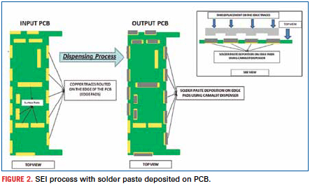
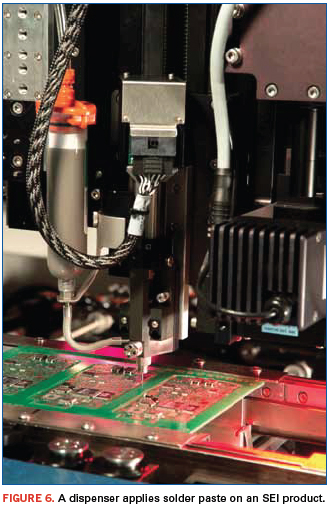
This new SMT process has been demonstrated to facilitate new space-saving attachment designs, while creating a robust soldered connection for SEI along the vertical surface of the outer edge of the PCB. Solder paste is dispensed onto the bare copper pads of the PCB along the traces or the perimeter where the shield will be placed. Here, the authors describe the process steps using dispensing for SEI.
Current shield placement techniques. Shield attachment to date has involved either of two methods. In the first method, a “metallic fence” is formed around the perimeter of the area to be shielded. Then a spring-loaded “metallic lid” is snapped over the fence to enclose the area. The mechanical contact between lid and fence creates the shield. In the second approach, solder paste is applied to the bare copper pads of the PCB along the traces or the perimeter where the shield is to be placed. The shield is then placed and soldered using standard reflow process. This is a one-step process. This latter approach has gained considerable popularity because it cuts out a process step and requires less PCB real estate.
SEI process. The key to a successful SEI process is to uniformly dispense a controlled amount of solder paste accurately at the edge location to provide the optimum shield interconnection. Properly implemented, the process will dispense paste on the edge copper traces such that 50% of the solder volume is on the top of the edge pad, and the remaining 50% is deposited on the side trace of the edge pad for good bonding between the shield and substrate edge. As such, the typical dispensing is in close proximity to the edge of the PCB, which creates a unique challenge. This is addressed through use of a traditional auger pump controlled by software that handles edge detection (of the PCB) for high process accuracy and controls dispensed line width.
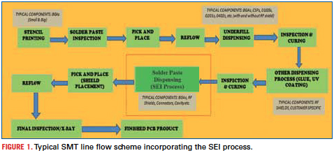
The inherent simplification of the one-step shield attachment process also creates a complete metallic (solder) bond surrounding the entire PCB that makes the RF shield highly reliable. Low-temperature Pb-free (no-clean) solder alloys are used to attach RF shields. This is because an SMT PCB assembly that includes RF shields undergoes two reflow passes: the first to attach the SMT components, and the second to attach the RF shields. Although the first pass will typically involve higher-temperature Pb-free solder (e.g., SN100C @ 227°C) to form the solder joints for the component leads, one does not want those solder joints to see liquidus or even near-liquidus temperatures a second time due to the potential for oxidation degradation, dewetting, and other problems. It is also desirable to limit the degree of thermal cycling of the board to minimize potential for damage associated with thermal stress. Consequently, second-pass reflow for shield attach is achieved using low-temperature melting alloys, such as a SnBiAg alloy with a melting temperature point below 140°C. Figure 1 shows a typical flow scheme whereby the PCB is assembled with components and reflowed in the standard manner. Following those process steps, the low-temperature solder paste for shield attach is dispensed; the shield is put in place, and the assembly is reflowed.
As mentioned, the nature of the SEI process in the SMT line is compatible with and provides advantages to other dispensing applications such as underfill, where dispensing systems can implement the underfill process without the presence of RF shield cans on the PCB. This provides a significant advantage to the underfill process, as restrictions on underfilling through the RF shield holes designed by the OEMs can be avoided.
Technology considerations for SEI. Key process control parameters essential to achieve SEI include the following:
- Precise control of solder volume dispensed per pad/interconnect area.
- PCB edge sensing accuracy – absolutely critical for this atypical dispense application.
- Ability to dispense varying solder paste types (including types 3 through 6).
- Ability to dispense pastes via varying needle sizes (IDs).
- Precise line (solder bead) width dispense accuracy.
- Repeatable consistency of deposition over high volume/throughput.
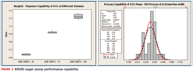
Establishing pump capability is key in developing a robust process for SEI. The Camalot Model 635 Servo Drive (SD) pump, an auger-based system, was chosen for this application. Capability analysis (Cpk) of the pump is conducted on line widths measured by dispensing different solder volumes or bead widths. Data are statistically validated with variability plots of multiple line widths (Figure 3). Results presented in Figure 3 have shown the pump capability with tolerance of 10% over average or target given by the customer. This precision is critical to the SEI process, since high variability in solder volumes can result in serious failure defects, including shorts and opens, as most of the lines are dispensed on the edge pads of the PCB where solder volume and solder bead width are critical. Such qualification was necessary in proving the suitability of this auger pump model for the SEI process.
The dispense platform chosen for SEI process development was the Camalot Prodigy, which has an accuracy of +/-35µm at 3Σ, and repeatability of +/-10µm at 3Σ. This is supported by acceleration speeds of 1.5g in motion to dispense packaging materials at independent locations.
Software capability is critical to effectively program dispense locations based on the design of the PCB and dispense requirements. “Line dispense” commands with parameters aligned to the auger pump capabilities are used to design the dispensing process. With the SEI application the challenge is to address the dispensing process for the edge pads, as the coverage area is unique to traditional solder paste dispensing. This is where a new feature that is based on vision algorithm drives to accurately locate the edge pads of the PCB and ensure accurate dispensing with optimum solder paste coverage.
Finding the edge. A state-of-the art vision system was developed to provide the vision capabilities required by SEI. The camera system used is equipped with digital vision enhancement with sub-pixel definition. These hardware enhancements maximize the accuracy of the fiducial locations, components and pad edges, to provide additional features, including visual inspection for automatic deposition monitoring.
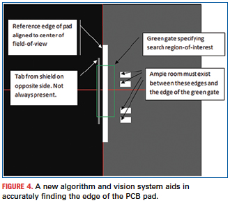
The primary objective is to permit the vision system to find the edges of the PCB accurately. To execute this feature, a command is used in which the user teaches the edge pads of interest. This command for edge find uses the same options as used for a standard fiducial, but instead we teach the edge of the copper pad. Figure 4 shows how a sample template appears with respect to a PCB edge pad. This figure also depicts the edge pad of the PCB with and without the RF shield on the other side, in case the SEI process requires shielding on both sides of the PCB. The software and vision capabilities show the different options for the user to teach the pad accurately. The vision system and software has the ability to distinguish the edge pad from the shield, if there is a shield present outside the edge pad, and accurately dispense on the edge of the pad.
Once the edge pads are taught, the software and vision move to that position at the beginning of the SEI process and search for the second edge of the pad to trace a complete edge. Figure 5 provides a snapshot of how the software executes the search algorithm.
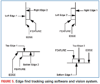
Figure 5 shows the edge of the PCB is traced by teaching the position of the edge pad on the PCB. If the edge pad is located on the left-hand edge of the PCB, the user selects a command to look for the second edge coming from the right to left side of the PCB. If the edge pad is located on the top edge of the PCB, the user selects a command to look for the second edge coming from the bottom to top side of the PCB. Similarly, different edge pads at different locations can be taught by the user, using the locate edge feature in the process program. It is highly recommended that the locate edge feature always be taught in pairs. The software has the capability of teaching multiple edge pads to have higher accuracy and accounts for manufacturing variability such as shape, size and discoloration.
Next, in similar fashion to the standard “dot” or “line” command, the user teaches the machine to apply the line or dot. However, in this case, the line or dot will use the reference position as the edge of the pad or PCB, such that 50% of solder volume is on top of the pad and 50% on the side of the pad. The process herein described is critical to the dispense quality along the edge pads for the SEI process.
The combination of the vision system for edge pad recognition with algorithms developed within the software enables a 9 or 13µm per pixel resolution, necessary for the vision to detect edge pads and other pads as small as 50µm in width or diameter. The combined technology takes into account the variability of the edge pad shapes, where a less-than-ideally shaped edge pad could still be detected by the vision system to ensure the right volume of solder paste is dispensed.
Line width measurement and line width adjustment features are critical to the SEI process. For this purpose, a template is designed to input some dispense parameters for dispensing lines. The pump automatically dispenses the line on the pre-dispense area, and the vision system inspects the line to compute the bead width. Line width adjustment monitors the accuracy of the amount of material dispensed and makes adjustments automatically if line widths are found out of tolerance or specification limits. This feature presents a process monitoring system critical to large-volume production.
SEI application using automated solder paste dispensing is a robust process that depends on strict process control. Implementation depends on specific capabilities in the dispenser, pump, vision system and software relative to line-width control and edge-definition capabilities. It creates a sufficiently durable RF shield connection to be suitable for mobile personal communication device assembly delivering products of high quality.
Rajiv L. Iyer is an applications engineer III at Speedline Technologies; riyer@speedlinetech.com. Michael Martel is a product marketing engineer at Speedline.

Before blaming the placement accuracy, check for board vibration.
Figure 1 shows the misplacement of a package-on-package after dipping the balls in dip paste and reflowing the assembly. The solder paste has successfully reflowed and coalesced with the solder balls on the PoP. However, as the image shows, lifting the device reveals no solder joints on the pads. The clear rings of flux residues on the surface of the solder mask show only that the flux from the paste has been left behind.
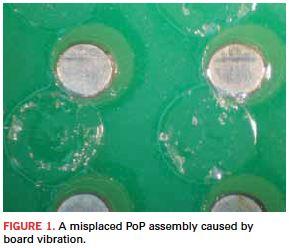
Misplacement of the device could have occurred after placement or during reflow due to board movement or vibration. It would be fairly simple for the part to be repositioned and soldered in place with suitable rework equipment.
These are typical defects shown in the National Physical Laboratory’s interactive assembly and soldering defects database. The database (http://defectsdatabase.npl.co.uk), available to all this publication’s readers, allows engineers to search and view countless defects and solutions, or to submit defects online. To complement the defect of the month, NPL features the “Defect Video of the Month,” presented online by Bob Willis. This describes over 20 different failure modes, many with video examples of the defect occurring in real time.
Chris Hunt is with the National Physical Laboratory Industry and Innovation division (npl.co.uk); chris.hunt@npl.co.uk. His column appears monthly.
SnCuNi soldering performance at low temperatures.
Nickel-modified tin-copper solder, known commercially as Sn100C, is a leading lead-free alloy for PTH soldering, rework and hot air-leveled PCB final finishes. Because it contains no silver, it is much more economical than SAC alloys containing as little as 1% of the precious metal, and it produces smooth, shiny, easy-to-inspect solder joints. Why has it not gained major acceptance as an SMT alloy? In large part, fear. Fear of full compatibility with SAC reflow processes.
SnCuNi melts at 227°C. SAC 305 begins to melt at 217°C, reaching its fully liquid state at approximately 220.6°C. Recommended reflow temperatures are typically at least 13°C higher than melting temperatures, hence the SAC 305 peak temperature window of 233° to 255°C. Applying the 13°C guideline to the SnCuNi alloy results in a minimum peak temperature recommendation of 240°C. It’s that 7°C difference in minimum reflow temperatures that generates the fear – of cold joints, incomplete wetting, inconsistent IMC formation or other reliability issues – if the peak temperature of a solder joint falls into that questionable space between 233° and 240°C.
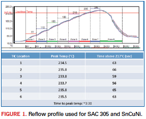
Laboratory tests have demonstrated good wetting at lower temperatures, but they’re just that: lab tests. Until recently, there was no real-world, production-based data on the soldering behavior of the SnCuNi alloy near the low margin of the reflow window. But a newly published study1 explored exactly that situation. It dropped the Sn100C alloy into a reflow process considered cool for SAC 305; the temperature peaked at 234°C with only 60 sec. above 217°. The cool process shown in Figure 1 was dictated by thermally sensitive components on the PCB, which was a mixed-technology industrial controller of low-medium complexity.
The experiment consisted of two runs, one with SAC 305 solder paste and one with SnCuNi solder paste. Thirty boards of each were built. Both pastes used the same flux, and the two products ran down the assembly line sequentially with no changes to any portion of the SMT process. Following assembly, the boards were subjected to numerous tests and analyses.
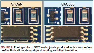
Inspection and electrical test. AOI took place on the assembly line, and visual inspection was performed by the line’s IPC-certified inspectors. No defects were found by either inspection process. The SnCuNi solder joints formed under the cooler profile did not exhibit the typical luster that is characteristic of the alloy, but were not as dull as SAC 305. Figure 2 shows photos of the typical solder joints produced in this process.
Five PCBs from each alloy group were then fully assembled with PTH, wave-soldered, and installed into chasses for functional test. They all passed, and the assemblies were earmarked for thermal cycling.
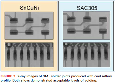
X-ray analysis showed more voiding in the SnCuNi solder joints than the SAC 305 (Figure 3). Although the voiding levels are acceptable, they could likely be mitigated by adding a soak to the reflow profile.
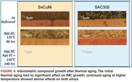
Microstructural analysis. Optical microscopy showed good wetting to both leaded and leadless terminations, and good IMC formation. In the as-reflowed state, both alloys formed continuous IMCs approximately 3µm thick. They were then subjected to two thermal aging cycles: an initial one at 125°C for 96 hr. and a subsequent cycle at 150°C for 240 hr. The initial cycle had no significant effects on the IMC or the solder joint shear strength. Both alloys demonstrated similar IMC growth during the second aging (Figure 4).
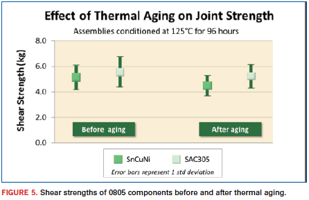
Joint strength. Next, 0805 components were shear tested at 15° angles before and after thermal aging. Shear strengths averaged 4 to 6kg, typical for this component size and comparable to previous tests run on assemblies with peak temperatures of 245°C. Thermal aging had no significant impact on shear strength values (Figure 5).
Thermal cycling. Original experimental plans included thermal cycling five full assemblies from each alloy set. However, given the good appearance, microstructure and solder joint strength, it is highly unlikely any solder joints would fail during cycling, and no new knowledge would be gained from the effort. A similar study that compared the two alloys on a more complex PCB completed 3000 cycles (0° to 100°C) with no remarkable results. Therefore, thermal cycling was eventually eliminated from the test plan.
The results of this test were eye-opening. A reflow process with a peak temperature of only 234°C and 60 sec. above 217°C is considered the low end of the window for SAC 305. Despite SnCuNi’s higher melting point, it formed good joints, passing every standard test to which it was subjected. It demonstrated full compatibility with the cool range of the SAC 305 window, establishing itself as a viable drop-in replacement for almost any SAC-based SMT process.
The silver-free alloy is currently used in numerous consumer applications, but concerns over low temperature reflow processing have slowed broader implementation
and delayed its resulting cost reductions, which can be substantial. Replacing SAC 305 with SnCuNi can save as much as 20% on solder paste costs due to the elimination of silver.
This study was instrumental in generating production-based data for the previously uncharted area of the reflow window. It should help to dispel fears of poor reliability if SnCuNi is soldered on the low end of the established SAC 305 process. Many thanks to Andy Monson and Walter Machado of Hayward Industries for making this experiment possible and sharing the results with the industry.
References
1. The data presented here are part of a larger study presented and published at SMTA International; it can be downloaded at http://www.aimsolder.com/technical-articles or at http://www.CircuitsAssembly.com.
Karl Seelig is vice president of technology at AIM Solder; kseelig@aimsolder.com. Tim O’Neill is regional manager at AIM.
Embedded Design
“Interfacing PIC Microcontrollers: Embedded Design by Interactive Simulation”
Author: Martin P. Bates; mbates@hastings.ac.uk.
Abstract: The second edition of this book is an introductory text for those starting out in this field and a source reference for more experienced engineers, containing a balance of theory and practice with numerous working examples throughout. It provides comprehensive coverage of basic microcontroller system interfacing using the latest interactive software, Proteus VSM, which allows real-time simulation of microcontroller based designs and supports the development of new applications from initial concept to final testing and deployment. It includes a comprehensive introduction to interfacing 8-bit PIC microcontrollers; designs updated for current software versions MPLAB v8 & Proteus VSM v8; and additional applications in wireless communications, intelligent sensors and more. (Elsevier, October 2013)
Optical Waveguides
“Influence of Photolithography on the Cross-Sectional Shape of Polysiloxane as an Optical Waveguide Material on Printed Circuit Boards”
Authors: Dr. Kam-chuen Yung, et al.; mfkcyung@polyu.edu.hk.
Abstract: Optical waveguide cross-sectional shapes that deviate from rectangles or squares may cause significant loss of signal. In this study, a photolithography approach was adopted to fabricate waveguides on PCBs, using photo imageable polysiloxane as a waveguide material. The effects of I-line ultraviolet (UV) lamp exposure, 355nm Nd:YAG laser direct imaging, and 248nm excimer laser direct imaging on the cross-sectional shape of waveguides were investigated. For I-line UV lamp exposure, increasing the exposure time could cause changes in the tilt angle of the waveguides from negative (inverted trapezoid) to positive (trapezoid). To obtain rectangular waveguides, the optimum I-line UV lamp exposure time was found to be around 150 sec. From the results for 355nm Nd:YAG laser direct imaging, the width and tilt angle of the waveguides varied with the energy density of the laser beam irradiating the core materials, being controlled by the repetition rate and focus. Lowering the laser energy density could produce waveguides with small widths and tilt angles. Excimer laser direct imaging at 248nm was found to be unsuitable for waveguide patterning since the core materials could not be cured at this wavelength. (Journal of Electronic Materials, December 2013)
Printing
“Plasma Stencil Treatments: A Statistical Evaluation”
Authors: Matt Kelly, William Green, Marie Cole and Ruediger Kellmann; mattk@ca.ibm.com.
Abstract: Integration of large and small body components onto a single PCB with increasing population densities and tighter placement spacings, drives the need for consistent solder paste print deposits to ensure maximum first-pass assembly yields and highest product quality/reliability levels. Balancing solder paste printing of large and small print deposits has been reported to be enhanced using various surface treatments on laser-cut stencils. This study focused on examining the effects of a plasma coating compared to conventional stainless steel laser-cut technology. Printing performance on a variety of components was evaluated including five different BGAs, flip-chip QFNs, SMT electrolytic capacitors, 0805, 0402, and 0201 passives. Lead-free no-clean and water-soluble paste chemistries were included, along with two different aperture ratio (A/R) design points for all components studied. For assessing the durability of the plasma coating, production volume cleaning simulations were conducted with 24 different solvents.
Statistical analysis was conducted to evaluate any observed differences between conventional stencil technology and a plasma-treated alternative. A DoE was conducted to evaluate main effects and interactions. (SMTA Journal, vol. 26, no. 4, Winter 2013)
Solder Materials
“Thermal Conductivity Variation with Temperature for Lead-Free Ternary Eutectic Solders”
Authors: Namık Aksöz, et al.
Abstract: Variations of the thermal conductivity with temperature for the lead-free ternary eutectic solders Bi-42.73 wt.%Sn-1.03 wt.%Ag (Bi-Sn-Ag), Sn-3.5 wt.%Ag-0.9 wt.%Cu (Sn-Ag-Cu), Sn-6 wt.%Sb-5 wt.%Ag (Sn-Sb-Ag), Sn-42.8 wt.%Bi-0.04 wt.%Cu (Sn-Bi-Cu), and In-48.4 wt.%Sn-2.31 wt.%Ag (In-Sn-Ag) were measured using a linear heat flow apparatus. It was observed that the thermal conductivities of solid phases for the BiSnAg, SnAgCu, SnSbAg, SnBiCu, and InSnAg solders decrease linearly with increasing temperature. Thermal conductivities of the BiSnAg, SnAgCu, SnSbAg, SnBiCu, and InSnAg solders at their melting temperature were obtained as 17.89 ± 1.6 W/K-m, 49.89 ±4.5 W/K-m, 41.96 ±3.8 W/K-m, 20.03 ±1.8 W/K-m, and 70.21 ±6.3 W/K-m, respectively. Thermal temperature coefficients for BiSnAg, SnAgCu, SnSbAg, SnBiCu and InSnAg solders were determined to be −2.894 × 10⁻³ K−1, −0.907 × 10⁻³ K−1, −1.246 × 10⁻³ K−1, −2.638 × 10⁻³ K−1, and −1.250 × 10⁻³ K−1, respectively, from plots of thermal conductivity versus temperature. (Journal of Electronic Materials, December 2013)
This column provides abstracts from recent industry conferences and company white papers. Our goal is to provide an added opportunity for readers to keep abreast of technology and business trends.
A look back at friends and colleagues who left us in 2013.
Anyone who has walked through what used to be called a stereo store over the past 50 years has at some time no doubt heard music blaring from a Kenwood or Bose speaker. Bill Kasuga, who cofounded the latter, and Dr. Amar Bose, the genius behind the eponymously named Bose Corp, both left us this year, though their companies live on.
Other significant inventors who passed away were Dr. John E. Karlin, the Bell Labs engineer who designed the first touchtone phone keypad, and Gunter Erdmann, who held 13 patents for electronics materials and solder printing.
This year was particularly sad for the staff of UP Media, as we lost one of our own, Jerry Murray. Murray, the longtime West Coast editor for Circuits Assembly and PC FAB, passed away Jan. 13.
This month we reflect on their impact on our industry and our lives.
- Lance Redfearn, 48, territory account manager at MetricTest.
- Phillip D. Hester, senior vice president of R&D, National Instruments, and holder of more than 10 patents in microprocessor technology.
- Bill Kasuga, 98, cofounder of Kenwood Electronics.

- David Weissman, 59, president, Precision Graphics.
- Dr. Amar G. Bose, founder Bose Corp. and former Massachusetts Institute of Technology professor.

- Rob Tyrrell, 62, technical director, StenTech.

- Jack McCann, 54, president, Mega Fluid Systems.
- Dr. Jim Arnold, 63, longtime engineer AT&T Bell Labs and Motorola, and iNEMI consultant.

- Liu Fuzon, 14, 3CEMS factory worker.
- Milo Bryant, 82, Ayrshire Electronics chairman and chief executive.
- Jerry Murray, 82, Circuits Assembly and PCD&F West Coast editor, mentor and friend.
- Gunter Erdmann, 73, former president of MPM, invented the reciprocating squeegee, and held patents on solder paste and stencil frames.
- Seven unnamed Foxconn workers.
- Dr. John E. Karlin, 94, Bell Labs industrial psychologist and electrical engineer, designed the touchtone phone keypad.
- Glenn L. Seely, 56, sales and marketing manager at Southwest Systems Technology, Austin American Technology, and president of Alandra Services, a manufacturer’s rep company.

- Fred Hübner, 62, managing partner of GSS Grundig SAT Systems and ZVEI Satellite & Cable board member.
- Kenny Keegan, 53, sales engineer, Sager Electronics and TTI.
- Bill Henningsgaard, 54, former Microsoft executive.
- Dick Topping, 78, longtime sales representative for BTU and other electronics companies.
- Eric Lidow, 100, cofounder, International Rectifier.
- Paul Blanchette, 61, veteran IBM packaging engineer.

Who says a Tier IV EMS can’t have the foresight, and follow-through, of the big players?
Small tier EMS companies face many challenges, not the least of which is the ability to attract good workers and the access to capital to stay competitive. Generally, they don’t spend a lot of time thinking about models; that’s a practice for larger firms in which the executives don’t also spend time running the lines.
What small firms do understand, almost intuitively, is they can’t pay lip service to service. Speed counts. And niches count. Indeed, one could argue service, in itself, is a niche. SMT equipment, while sophisticated and highly engineered, is after all available to anyone who has the right amount of funds.
In that respect, Lightspeed Manufacturing has two niches. Its technical expertise lies in rework of ball grid arrays and other higher value components and assemblies.
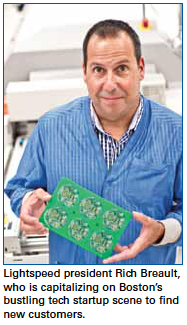
And there’s the service component: President and founder Rich Breault has never met an order he wouldn’t turn around in 24 hours or fewer. He is a relentless ball of energy who spends hours each day talking with customers, suppliers, competitors, and just about anyone else in the industry who will answer their phone.
Based in Haverhill, MA, about 35 miles north of Boston, Lightspeed has been keeping other companies’ boards out of the scrap pile since 2003. (Breault also founded Netco, another Haverhill-based EMS, which he sold to Chase Corp. in 2000.) Its customers range from OEMs in the computing, defense, industrial, and more recently, aerospace end-markets, to other EMS companies, some large, some small. Lightspeed has customers throughout the Eastern seaboard.
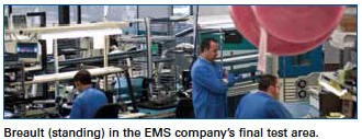
The 8,800 sq. ft. factory maximizes its use of space, with hardly a square inch of vacant real estate to be found. In it are two full SMT lines, featuring DEK printers, Mydata placement machines, and Speedline Electrovert convection reflow. An SPI is next. Offline is x-ray and functional test. Breault keeps a close eye on spending, buying mostly gently used equipment, often at auction, and, if the price is right, occasionally well in advance of when he thinks he will need it.
During the past few years, Lightspeed has added more mechanical build and enclosure capability.
When we first toured Lightspeed in 2005, Breault explained that his goal was to take advantage of the high-flying Boston tech community by finding and teaming with an entrepreneur, perhaps one emerging from MIT or Harvard, and grow alongside them. His patience has begun to pay off.
In 2012, Lightspeed aided a program called the Haverhill Hardware Horizons Challenge, a local effort to highlight potential engineered products, by offering several prototypes to the winners of the content. He then hooked up with MassChallenge, a larger and global accelerator program based in Boston. Lightspeed put a small lab inside the MassChallenge headquarters, giving Breault access to scores of entrepreneurs, many of whom had ideas for new hardware. There, Lightspeed provides production engineering assistance, along with a full bench of equipment, including soldering irons, Solidworks and AutoCAD software, a Sciencescope meter. One
exception: a Formlabs 3D printer.
When MassChallenge moves next spring to a larger building, the Lightspeed Innovation Lab will grow with it. This time, Breault plans to put a full SMT line, including two Quad placement machines, a drill press and belt sander for mockups, hand soldering tools and other equipment on the same floor as the Challenge workspace, and staff it with a full-time operator, thus adding another level of capability (and giving himself a captive market of potential customers).
Through his connection with MassChallenge, Breault has landed four new accounts, including Bounce Imaging. Bounce is inventor of the Explorer, a low-cost handheld device full of embedded cameras and sensors that can be rolled into a dangerous environment in order to collect reams of data ranging from photos to temperature and CO readings, thus helping humans learn about – and avoid – potentially hazardous situations. The invention has been lauded by Popular Science and Time, among others. Bounce’s cofounder, Francisco Aguilar, says Lightspeed has been “essential” to Bounce’s success. “We could have been working on this for years. But it’s not just a question of time saved. We wouldn’t be if it weren’t for the MassChallenge and Lightspeed Manufacturing,” he says.
“We think that all this innovation comes from big companies with huge R&D budgets,” Breault notes wryly. “And in doing so we forget how innovation always changes things and levels the playing field. Through the MassChallenge, we constantly ask, ‘How do we help entrepreneurs build their dreams? And how do we get the ideas to reality and to market?’ ”
Too much growth too fast has foiled many an EMS player. The success of new customers like Bounce might push Lightspeed in ways the company isn’t currently designed to handle. In the event that Breault can’t keep up with a company that hits it big, he has a backup plan. “We want to partner with a Tier 1 to help them ramp,” he says. “And we want to partner with a machine shop and plastic injection molding manufacturer too.”
Breault sees a potential side benefit to the partnership as well: accomplishing big social goals. “My goal is to bring manufacturing jobs back to the inner city.” This shows unusually sharp and forward-looking vision for a small company.
In the six-year history of the CIRCUITS ASSEMBLY EMS Company of the Year, we have never selected a small tier company. It’s difficult for small companies to truly distinguish themselves. It’s even harder for them to establish a model and culture that can withstand changes in ownership. Whether Lightspeed could perform the way they do without Breault’s leadership remains to be seen. But his vision and execution has been sustained and extraordinary. And that’s why Lightspeed Manufacturing is our EMS Company of the Year for 2013.
Mike Buetow is editor in chief of CIRCUITS ASSEMBLY; mbuetow@upmediagroup.com.
Ed.: For a related article on MassChallenge, click here.

Press Releases
- Zollner Puts a New Mechanics Building into Operation
- Changes in Incap’s Management Team: Incap updates its leadership model to support its growth strategy
- Niche Electronics Celebrates Completion of Florida Expansion
- Microscreen Names Nik Thomas Director, Expands Leadership Role Amid Continued Organizational Growth