

The good designer acts as referee, heading off poor instructions and ill-advised engineering.
Design for assembly (DfA) is an ongoing struggle to balance assembly, fabrication and layout. The layout designer strives to create a product with ease of assembly in mind. To design the best assembly, the layout designer needs to understand the fabrication limitations of the components and the fabricator. The layout designer is a mediator between the requirements of the engineer, the fabricator’s abilities and the needs of assembly.
Footprint accuracy is the single most destructive mistake a layout designer or engineer can make. The component specs are not standardized. Footprint drawings are not always to scale. Some specs are drawn from a bottom view as opposed to a top view. Many components do not fit on the manufacturer-recommended footprint. The controlling dimensions are not always clear.
Using a CAD tool built to verify footprints can save schedules and rework. These tools have the ability to build a model to the dimensions of the component. The tool is able to overlay the model of the physical component over the footprint generated in the design tool. Using the latest spec ensures that the component is the latest revision.
The DfA check covers pin pitch (Figure 1), row pitch (Figure 2), pin type, component spacing, pin toe and heel (Figure 3), pin width (Figure 4) and overall assembly review. Any one of these items can delay a schedule or cause unattractive rework on a board. Many of the issues will scrap a complete lot of PCBs (Figure 5).


Pin pitch mistakes typically are made during the conversion from mils to mm or vice versa. The other error made is not identifying the correct controlling dimensions. The majority of mechanical drawings will include the controlling dimensions. Pin pitch is a cumulative error. On low pin count items, it rarely is a problem. The more pins a device contains, the larger the cumulative error becomes.
Row pitch does not suffer the same ability for cumulative errors, except on multi-row/column components. Ball grid arrays and connectors should be built in the original dimensions. Row pitch on quads can force a designer to use smaller pads on the corners or increase the toe while decreasing the heel of the solder joint.
Typically, pin type is a mistake that is made during the component lookup or a late BoM change. The manufacturer part specs are accurate between SMT and through-hole pins. The conflict arises on mounting holes. Many manufacturer specs do not indicate if the mounting pins are plated or non-plated. Press-fit pins require a tighter tolerance and should be noted in the fabrication and assembly drawings. Component spacing affects the initial placement and the amount of rework effort. BGAs require room for rework, or the surrounding components will need to be removed before the BGAs can be removed.
Pin toe and heel are critical for a solid solder joint. According to Texas Instruments’ solder pad recommendations for surface mount devices, the criteria for a well-designed solder joint are based on both empirical data and reliability testing. Solder joint strength is directly related to the total solder volume. A joint can be described by the solder fillets formed between the device pins and the PCB pads.
Pin width also is a factor to consider. The expected assembly process will help determine the width variations for the pin width increase. Boards that will be wave-soldered will need a wider pad than those that are reflowed. A major concern when making the pads wider is the solder mask webbing, which prevents shorts.
DfA is continuous process in which assembly, fabrication and layout must all work together. Understanding the requirements of each is key to creating a successful, smoothly running assembly. The layout designer plays an important role in this, acting as a mediator between the engineer, fabrication shop and assembly needs.
W. Scott Fillebrown is president and CEO of ACD (scott.fillebrown@acdusa.com). His column runs bimonthly.
How a seemingly simple soldering issue led to a host of process questions.
Just the other day I was walking through the maze of cubes that I call home when an interesting comment caught my ear. The conversation was on how to solder a wire to a flexible printed circuit. How could it be possible that in this day and age when FPC assembly is common, and at times quite advanced, there would be a need to discuss how to solder a wire to an FPC? As I listened, it became clear this was not an ordinary solder-the-wire-to-a-board application. This was a micro-coax cable terminated to the FPC through solder joints to the copper circuitry directly, rather than through a board-mounted connector.
Let me frame the application: We wanted to take advantage of a very thin multilayer circuit populated with active and passive components in order to fit the interconnect into an extremely thin device – a perfect application for an FPCA. The trouble was, the micro-coax (coaxial) cable was the thickest component in the assembly, and the associated solder joint height was driving the overall Z height of the FPCA beyond the devices’ height requirement. How did we solve this? Let me walk you through some of the techniques we tried in order to reduce FPCA thickness, and share the solution we ultimately used.
Here’s our parameters:
- Both the inner cable and outer conductor required a solder connection.
- The solder height requirement was 80µm max.
- The gap between inner cable and solder pad needed to be reduced as much as possible.
- We needed to produce 150,000 per week.
Here are the choices we considered:
Good old-fashioned hand soldering. Hand soldering was used for the first design verification run. We knew it lacks the capability or volume scale needed for the final production unit, but it did allow us to get parts to the customer to start design evaluation, while we continued our evaluation of available processing options that exhibit solder volume.
Surface mount technology. SMT process for solder paste and reflow is the industry standard, exhibiting controlled paste volume, accurate paste placement, and appropriate throughput/cost for mass production. I had thought this would be the ideal solution, as the FPCA had many other components to be mounted on the side where the coax cable was located, and the wire would have been placed after those other SMT-placed components, but there was one bump in the road that prohibited us from using solder paste and reflow for the coax cable. The design required the cable to lie over the top of other components, which meant the coax cable could potentially move other components off their respective pads during reflow.
Laser soldering. Once mass soldering was ruled out, our options for connecting the coax cable with a secondary operation were reduced to some process of soldering individual wires. With hand soldering unable to meet our volume requirement costs, we suggested another automated option: lasers. Laser soldering tools are fantastic for soldering components that cannot withstand the soldering temperature of the reflow oven; are significantly larger than the surrounding components, causing thermal management issues during reflow of the smaller components, or as in this case, where overlapping placement of components is required, resulting in a secondary attach operation. Process control is also a strong point for laser soldering. Optical alignment ensures the laser energy is placed at the same location every time, and the amount of solder dispensed can be tightly controlled.
While laser soldering is a highly controlled, automated process, the difficulty is presenting the board and component to the laser machine so it can solder the joint. Our issue was with designing fixtures and tools that could effectively handle the thin FPCA and present both ends of the coax cable for soldering. We found that we could effectively present the outer solder joint for soldering, but we couldn’t get the inner joint to connect. Since the inner conductor did not always make contact with the solder pad (see “gap” in Figure 1), and our fixture solutions wouldn’t be able to close that gap mechanically, we thought to dispense a larger amount of solder to compensate for the gap between the inner cable and pad. By doing this, the solder joint height was growing beyond the 80µm maximum allowable height. Faced with a very complex tooling and fixturing problem that was bound to take a lot of time to develop, cost a lot of money, and require a level of complexity that introduces variation, we decided to look at other soldering options.

Robotic soldering. Robotic soldering is very similar to the laser in that a solder tip is used to make the joint. The agility of the robotic arm and the optically located solder point ensures consistent, accurate joint placement. As with laser soldering, solder volume is tightly controlled and consistent from joint to joint. The main benefit of robotic soldering over laser, in this case, was that the solder tip could be used to push the inner end of the cable to make contact with the solder pad before soldering. With the mechanical issue out of the way, we could optimize the amount of solder needed to make a good joint and avoid bumping up against the 80µm maximum allowable height requirement. Solder strength was tested by performing pull tests on the coax cable, showing 100% failures in the cable, not the solder joint. We had a winner.
The best solution. What I had thought was a simple question – How do I solder a cable to an FPC? – turned out to be a little more complicated. Each soldering technology we reviewed had its strengths and weaknesses. By matching the technology and process with the application, especially one in which we had only two solder joints per FPC with tight volumetric tolerances, we were able to pick the most reliable and overall cost-effective solution. This time, the winner was robotic soldering.
As the FPC becomes more universally accepted as a functional board with unique attributes – such as extreme thinness and 3D assembly considerations – this will not be the last time I hear a passing conversation with the words, “How do I do that?” for what was once a simple solution.
Dale Wesselmann is a product marketing manager at MFLEX (mflex.com); dwesselmann@mflex.com. His column runs bimonthly.
The cost of improving and maintaining reliability can be minimized by a model that quantifies the relationships between product cost-effectiveness and availability.
A repairable component (equipment, subsystem) is characterized by its availability, i.e., the ability of the item to perform its required function at or over a stated period of time. Availability can be defined also as the probability that the item (piece of equipment, system) is available to the user, when needed. A large and a complex system or a complicated piece of equipment that is supposed to be available to users for a long period of time (e.g., a switching system or a highly complex communication/transmission system, whose “end-to-end reliability,” including the performance of the software, is important), is characterized by an “operational availability.” This is defined as the probability that the system is available today and will be available to the user in the foreseeable future for the given period of time (see, e.g., Suhir1). High availability can be assured by the most effective combination of the adequate dependability (probability of non-failure) and repairability (probability that a failure, if any, is swiftly and effectively removed). Availability of a consumer product determines, to a great extent, customer satisfaction.
Intuitively, it is clear that the total reliability cost, defined as the sum of the cost for improving reliability and the cost of removing failures (repair), can be minimized, having in mind that the first cost category increases and the second cost category decreases with an increase in the reliability level (Figure 1)2. The objective of the analysis that follows is to quantify such an intuitively more or less obvious relationship and to show that the total cost of improving and maintaining reliability can be minimized.

Availability index. In the theory of reliability of repairable items, one can consider failures and restorations (repairs) as a flow of events that starts at random moments of time and lasts for random durations of time. Let us assume that failures are rare events, that the process of failures and restorations is characterized by a constant failure rate λ (steady-state portion of the bathtub curve), that the probability of occurrence of n failures during the time t follows the Poisson’s distribution  (1)
(1)
(see, e.g., Suhir1), that the restoration time t is an exponentially distributed random variable, so that its probability density distribution function is
 (2)
(2)
where the intensity
![]()
of the restoration process is reciprocal to the mean value of the process. The distribution (2) is particularly applicable when the restorations are carried out swiftly, and the number of restorations (repairs) reduces when their duration increases.
Let K(t) be the probability that the product is in the working condition, and k(t) is the probability that it is in the idle condition. When considering random processes with discrete states and continuous time, it is assumed that the transitions of the system S from the state si to the state sj are defined by transition probabilities λij. If the governing flow of events is of Poisson’s type, the random process is a Markovian process, and the probability of state pi(t) = P{S(t) = si,} i = 1,2...,n of such a process, i.e., the probability that the system S is in the state si at the moment of time t, can be found from the Kolmogorov’s equation (see, e.g., Suhir1) (3)
(3)
Applying this equation to the processes (1) and (2), one can obtain the following equations for the probabilities K(t) and k(t): (4)
(4)
The probability normalization condition requires that the relationship K(t) + k(t) =1 takes place for any moment of time. Then the probabilities K(t) and k(t) in the equations (4) can be separated: (5)
(5)
These equations have the following solutions:![]() (6)
(6)
The constant C of integration is determined from the initial conditions, depending on whether the item is in the working or in the idle condition at the initial moment of time. If it is in the working condition, the initial conditions K(0) = 1 and k(0) = 0 should be used, and
![]()
If the item is in the idle condition, the initial conditions K(0) = 0 and k(0) = 1 should be used, and
![]()
Thus, the availability function can be expressed as (7)
(7)
if the item is in the working condition at the initial moment of time, and as (8)
(8)
if the item is idle at the initial moment of time. The constant part (9)
(9)
of the equations (7) and (8) is known as availability index. It determines the percentage of time, in which the item is in workable (available) condition. In the formula (9),
![]()
is the mean time to failure, and
![]()
is the mean time to repair. If the system consists of many items, the formula (9) can be generalized as follows: (10)
(10)
Minimized reliability cost. Let us assume that the cost of achieving and improving reliability can be estimated based on an exponential formula![]() (11)
(11)
where R = MTTF is the reliability level, assessed, e.g., by the actual level of the MTTF; R0 is the specified MTTF value; CR(0) is the cost of achieving the R0 level of reliability, and r is the factor of the reliability improvement cost. Similarly, let us assume that the cost of reliability restoration (repair) also can be assessed by an exponential formula (12)
(12)
where CF(0) is the cost of restoring the product’s reliability, and f is the factor of the reliability restoration (repair) cost. The formula (12) reflects an assumption that the cost of repair is smaller for an item of higher reliability.
The total cost  (13)
(13)
has its minimum  (14)
(14)
when the minimization condition  is fulfilled. Let us further assume that the factor r of the reliability improvement cost is inversely proportional to the MTTF, and the factor f of the reliability restoration cost is inversely proportional to the MTTR. Then the formula (14) yields
 (16)
(16)
where the availability index K is expressed by the formula (9). This result establishes the relationship between the minimum total cost of achieving and maintaining (restoring) the adequate reliability level and the availability index. It quantifies the intuitively obvious fact that this cost depends on both the direct costs and the availability index. From (16) we have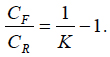 (17)
(17)
This formula indicates that if the availability index is high, the ratio of the cost of repairs to the cost aimed at improved reliability is low. When the availability index is low, this ratio is high. Again, this intuitively obvious result is quantified by the obtained simple relationship. The formula (16) can be used, particularly, to interpret the availability index from the cost-effectiveness point of view; the index reflects the ratio of the cost of improving reliability to the minimum total cost of the item associated with its reliability level.
The relationship between the availability index and cost-effectiveness of the product is quantified, assuming that the cost of improving reliability over its specified level increases, and the restoration (repair) cost decreases, when reliability level (assessed in our analysis by the mean-time-to-failure) increases. It has been shown that the total cost of improving and maintaining reliability can be minimized, and that such a minimized cost is inversely proportional to the availability index. The developed model can be of help when there is a need to minimize costs without compromising reliability.
References
1. E. Suhir, Applied Probability for Engineers and Scientists, McGraw-Hill, New York, 1997.
2. E. Suhir, R. Mahajan, A. Lucero and L. Bechou, “Probabilistic Design for Reliability (PDfR) and a Novel Approach to Qualification Testing (QT),” IEEE/AIAA Aerospace Conference, March 2012.
Ephraim Suhir, Ph.D., is Distinguished Member of Technical Staff (retired), Bell Laboratories’ Physical Sciences and Engineering Research Division, and is a professor with the University of California, Santa Cruz, University of Maryland, and ERS Co.; suhire@aol.com. Laurent Bechou, PH.D., is a professor at the University of Bordeaux IMS Laboratory, Reliability Group.
How one EMS company improved production time by shedding the straight line flow.
Two years ago, Orbit One decided to redesign its SMD line in Ronneby, Sweden, with the goal to decrease machines’ setup time or to increase uptime and shorten lead times.
The work started in 2010 when two “straight” production lines were reconfigured into a “U” shape, under the theory that this would minimize setup time and improve production flow.
To do so, we took two of our three lines and put them together. In other words, we took four placement machines and split assembly across the four modules, setting up the placement heads to assemble at the same time but just using half the number of feeders.
This way we shortened the lead time, and by using just one of the two feeder boards in the machines, we could perform a setup while simultaneously running the machines for the present job. That positively impacted uptime.
To optimize after this redesign, we adjusted the modules to balance the assembly time, which is of course important because the module with the longest assembly time determines the output from the machine. In theory it is simple, but it does require some effort from operators and programmers to make these movements between the modules. Depending on the design and number of components, some boards are harder to optimize. Also, other potential bottlenecks in the line, such as the screen printer or oven, must be considered.
Overall, the reconfigured line has been very successful. We produce with increased efficiency compared with the previous line configuration, and it’s easier to change production plans closer to the start date compared with the previous layout. Moreover, overall setup time has been decreased approximately 50%.
Per Jennel is sales and marketing manager at Orbit One (orbitone.se); per.jennel@orbitone.se.

Several key design rules are identified that require change from conventional design points.
Design for manufacturability (DfM) violations appear to be on the rise. Component placement densities are increasing, and printed circuit board sizes are maintained or decreasing. The result leads to increased component interactions during assembly and rework operations that can affect first-pass yields, quality levels, and product reliability performance. Increased product functionality using smaller form factors or provision for added functional content within a common and constrained pre-existing system form factor are the primary driving forces behind this trend.
Adding Pb-free assembly process constraints to these design trends further increases risks for quality issues, lower first-pass yields, and potential reliability issues. The higher temperature processing requirements, smaller process windows and increased mechanical fragility sensitivities associated with Pb-free assembly must be managed with utmost scrutiny when designing and assembling high-density complex hardware configurations.
Given these considerations, the need and opportunity to improve DfM management processes is clear. To ensure highest quality and reliability levels using new Pb-free-based materials, components, and processes, well-defined, collaborative, up-to-date, and efficient DfM practices are required.1
High-complexity server and storage hardware must be designed to maximize yields, quality and reliability performance. Because many server and storage class PCBs are high-dollar-value assets, they must be designed to enable rework operations, when needed. DfM reviews during early design stages help ensure product functionality requirements are attained, while ensuring the concept design can be properly manufactured and reworked.
With significant learning over the past six years, IBM has studied numerous DfM elements with the intent of determining what (if any) changes are required when migrating to Pb-free PCBs. Collective efforts have led to the identification of critical DfM elements that have indeed changed with the transition to Pb-free assembly, including:
- Printed circuit boards. Of critical importance is adhering to use of qualified PCB laminate materials and PCB constructions designed to survive maximum allowable temperatures, coupled with the use of preferred design structures for both ground plane thermal shielding and PTH devices.
- Temperature-sensitive components (TSC). To protect identified TSCs on a card assembly, special attention to TSC component selection, placement counts, and physical layout is required. As discussed in Pymento et al2 and Grosskopf et al3, TSC temperature and/or time violations can lead to reduced product field life. DfM reviews must therefore address these known TSC risk items.
- Component keep-out spacings. Minimum keep-out distances around components are required for several reasons, including rework nozzle and tooling needs, heatsink clearances, and minimization of adjacent/mirrored partial reflow during rework operations. Keep-out spacings apply to all component types, including SMT, PTH and compliant pin (CP) package constructions.
- New SMT pad geometries. SMT package styles continue to be introduced. DfM guidelines must therefore be optimized for new devices, including FC-QFNs, 0201 and 01005 passives, SMT DIMMs, and LGA hybrid sockets (to name a few).
- PTH component design elements. Conversion to alternate Pb-free alloys as published in Hamilton et al4 and Hamilton et al5 have led to many new DfM recommendations for PTH components, including finished barrel size, minimum remaining copper thickness, pin protrusion, and wave pallet design features.
- General PCB design elements. In some cases, design features that help to generally improve the manufacturability of PCBs may be mistakenly excluded from high-complexity design points. Some examples include the use of global fiducials, component polarity markings, and card edge keep-outs. Although considered very basic requirements, these elements may not always be included in designs, creating unnecessary challenges and longer process setup times during new product introduction activities.
Current Practice
OEMs have three primary options to control and manage DfM activities:
OEM ownership of DfM rules. In general, original equipment manufacturers can choose the option to continue investing resources to maintain internal DfM rules and processes. While some firms continue working in this traditional model, others do not. Some firms have offloaded all DfM responsibility to their contract manufacturers. Others use a collaborative approach with both firms working together to address DfM issues. It should be noted that if OEM firms decide to maintain ownership of DfM activities, sufficient resource and organizational structure must be allocated.
Industry standards. A second option is to use industry DfM standards. As documented by IPC6, there are five IPC documents relating to the design of PCB assemblies (Table 1). As shown in Table 1, four of the five have not been updated since the July 2006 promulgation of the EU RoHS Directive. Therefore, the majority of the documents do not contain any Pb-free content, nor is their coverage of component and PCB technologies up to date.
[Ed.: To enlarge the figure, right-click on it, then click View Image, then left-click on the figure.]

The exception here is IPC-7351B. This standard has been revised and does contain a variety of Pb-free additions. This said, there are still many key omissions within the document, including:
- SMT component design guide focus only.
- No rules for component keep-outs / spacings.
- No linkage to temperature-sensitive component risk points via J-STD-075.
- No PTH component design guidance.
- No compliant pin design guidance.
- No SMT connector design guidance.
- Lack of leading-edge component package styles.
Even with IPC-7351B now available, many contract manufacturers building server and storage hardware products opt for their own DfM rules. So although an industry standard exists in this case, it is not widely used.
Given that many of the industry DfM standards and guidelines are not being maintained, the limitations of IPC-7351B, and low IPC-7351B usage rates among contract manufacturers, utilizing industry standards to manage DfM activities does not seem the optimal solution.
Leveraging contract manufacturing partner protocols. As a third option, OEM firms can leverage their contract manufacturers’ skills and resources. Over the past 10 years, the majority of OEMs across many hardware product segments have outsourced manufacturing operations. With this shift, EMS firms now are primarily responsible for DfM reviews for new product introductions. Essentially, DfM activities that were once the responsibility of the OEM are now that of the EMS. As a result, OEMs are dependent on the performance of contract manufacturer DfM tools, capability and protocols.
While this option does help alleviate OEM resource and bandwidth issues, it also increases the risk of DfM control when an OEM is working with multiple contract manufacturers.
Many contract manufacturers offer DfM services as a differentiator among their competition. Therefore, DfM guides are usually considered confidential information and generally are not shared openly. For high-complexity hardware as found in server and storage systems, multiple card assemblies comprise the system architecture. Figure 1 shows a sample system comprised of:
- 15 PCB assemblies.
- 3 contract manufacturing locations.
- 3 different worldwide geographies.
- 3 different DfM guidelines / protocols (confidential).

In this example, multiple DfM rules and protocols exist and must be confidentially managed by the OEM. Although the final system sold to clients has an OEM logo, it is in this case built utilizing three different DfM protocols. It is therefore critical that OEM management of various DfM processes with contract manufacturers are well managed to protect quality and reliability levels expected by clients.
DfM Parameters for Optimal Pb-free Performance
To date, 21 specific DfM elements have been identified that are considered significant when converting to Pb-free-based assembly processes and design points. While optimal DfM parameters cannot be shared, Table 2 serves as a roster of focus items for the industry. To illustrate the importance of these design elements, the sections below discuss a primary DfM concern – component spacings (keep-outs) – along with a sample application to illustrate associated risks.
[Ed.: To enlarge the figure, right-click on it, then click View Image, then left-click on the figure.]

As shown in Figure 2, the keep-out area is defined as the additional area required around any component where no other component may be placed. Specified x/y linear distance is added to an existing component body dimension to calculate the resultant keep-out area. Although a typical BGA keep-out example is shown, it is important to note that such keep-outs are required for all component types, including SMT, PTH, and compliant pin technologies. Keep-outs help with assembly thermal and mechanical exposures affecting final product reliability, including:
SMT components:
- Local TSC protection during rework.
- Adjacent partial reflow protection (rework).
- Mirrored BGA rework challenges.
PTH components:
- Wave pallet chamfer keep-out designs.
- SMT and TSC component body solder exposures.
- Dendritic growth risks with unactivated fluxes (vias).
CP components:
- Nearby component mechanical force protection during CP assembly and rework operations.

Of equal importance, keep-out dimensions are required for a variety of assembly tools, including but not restricted to, component placement equipment, heat sink attachment process tools, hot gas rework nozzles, manual hand iron access, and ICT bed-of-nail fixtures.
As stated, with higher alloy melting and processing temperatures, smaller acceptable process windows, and increased mechanical fragility issues associated with Pb-free assembly, component keep-out areas have become of greater importance. This is especially true during Pb-free rework. While primary attach operations may not be significantly impacted by improperly designed keep-out areas, the ability for products to be reliably reworked may create significant challenges.
There are multiple reasons why products must be reworkable:
- Maximize first-pass yields and reduce scrap.
- Obsolete components.
- Supplier component recalls.
- Approved vendor listing changes.
- Product bill of material changes.
- Field failing components.
If rework is required (for whatever reason) operational efficiency, workmanship levels, quality levels, and reliability performance must be maintained.
If such component keep-out areas needed for rework are not well defined or implemented during design phase activities, then several consequences during new product development and/or volume production are likely:
- Inability to rework hardware quickly/efficiently.
- Increased reliability risks with reworked hardware.
- Added process development time required for complicated/non-ideal rework processes.
Figures 3, 4 and 5 illustrate several different component type keep-out area DfM violations as a result of increased component placement densities.
With the extremely tight spacing shown in Figure 3, the ability to rework the BGA device using a standard hot gas nozzle was not possible without special consideration of protecting the nearby DIMM connector. The solution in this case was the development of a specialty rework process that required nearly three months of development time.


Hand soldering iron rework access is illustrated in Figure 4. Passive or small body lead-frame components placed within connector arrays or too near large SMT connectors pose significant rework access issues and generally lead to lower workmanship and quality levels.
The last example (Figure 5) highlights the need for keep-out areas near PTH components. Since the temperature-sensitive component identified in red is within the designed PTH wave pallet chamfer opening, the component was originally exposed to molten solder during wave soldering operations. TSC component bodies are not generally rated to allow for Pb-free wave solder pot set point temperatures. Component movement outside the chamfer area was the solution in this case, requiring an additional circuit card design revision.
SMT component hot gas rework. If sufficient component keep-out areas are not integrated into designs, the ability for rework tooling and/or operators to access target rework components can be jeopardized. If the hardware design cannot be modified, complicated, multiple component rework processes are often required. If speciality rework processes are implemented, many technical risk elements must be carefully examined, including:
- Localized PCB damage, including delamination, solder mask/copper peeling, copper dissolution.
- Nearby temperature-sensitive component exposures.
- Excessive flux usage potentially leading to corrosion or dendritic growth.
- Partial solder joint reflow of same side adjacent and/or mirrored devices.
Figure 6 illustrates localized hot gas rework nozzle heat flows and highlights the key risk elements listed above. Figure 7 shows the same heat flow from a top side view perspective. The closer neighbor components are to the target rework site, the greater the risk additional defects can be introduced.


The BGA location shown in Figure 8 required hot gas rework. Due to increased system functional requirements, the assembly in this example included extremely tight component spacings. To access the target BGA device, seven nearby components first needed to be removed. As highlighted in the figure, the purple outline represents hot gas nozzle impingement; all components within this perimeter would first need to be removed. Once nearby components were removed, the target BGA device was removed, a new one added, then finally, all new perimeter components were added back, constituting a single rework cycle for the target BGA device.

Reduced throughput, added reliability risks, additional component costs, and additional engineering qualification activity resulted in this case due to the extremely tight component spacings defined in the original design point.
If nearby components were outside a well-defined keep-out area, then BGA rework operations for this case would be much lower risk and considered a business-as-usual process. Since keep-out dimensions were instead very tight, an expensive, slower throughput rework operation was required – adding quality, workmanship, and reliability risks to the process.
DfM priorities. Table 2 lists a significant number of DfM elements requiring action and optimization when migrating hardware to Pb-free constructions. As can be observed from the sample application, the complete DfM list encompasses a wide variety of technology elements, specification requirements, and design considerations. Extending these risk discussions to the other twenty items quickly demonstrates the need for optimized, collaborative DfM business processes between OEMs and contract manufacturers.
Traditionally, design groups tend to integrate design requirements with the following priority:
- Signal integrity.
- Power requirements.
- Cooling.
- Electronic card assembly/test manufacturability.
With the transition to Pb-free assembly, it is important to increase card manufacturability priority.
System-level management. Given the diversity of DfM control options, OEMs must consider when designing, procuring and fulfilling complex PCBs for subsequent high-reliability use in systems applications, it is extremely important to create a consistent DfM management review and communication process that can be used both early and often within the overall design, development, and hardware delivery cycles. This reoccurring review process is preferably used in three phases with a closed and interactive feedback loop between the OEM development organization, the OEM procurement organization, and the array of potential contract assembly organizations under consideration. The three general review phases preferably consist of the following general elements:
An initial phase involving a DfM review that occurs immediately after general board stack-up, PCB attribute selection, and general component floor planning activities have been defined by the OEM design and development teams, followed by second and third phases involving DfM reviews that occur during the assembler(s) selection cycle, and during the overall early hardware release-to-build cycle(s). Of critical importance within the early design cycle DfM review is for the PCB designer to be aware of key high-level design complexity attributes that may limit an assembler’s inherent ability to manufacture a given design, and to convey these critical attributes to assembly development and procurement organizations. By proceeding in this fashion, special process considerations, limitations, assembly risk, and special equipment needs can be clearly defined well in advance of actual assembly supplier selection.
In general, the scope of considerations includes identification of critical raw PCB attributes that may impact assembly reflow processes, and the general identification of critical components that may limit or restrict the scope of Pb-free SMT assembly operations that are viable for the supplier to implement, while ensuring assembly success and overall assembly reliability.
Using this process flow, subsequent DfM reviews that occur both at and beyond supplier selection stages can then preferably incorporate additional component-specific temperature sensitivity information and added details regarding necessary critical component assembly layout attributes referred to herein, while taking into account the various nuances associated with general assembly limitations identified from the initial and early design stage DfM evaluations.
Conclusions
As designs become denser, it is important for OEMs to conduct DfM reviews as early as possible in the design cycle to ensure that resultant server and storage class products can be built at the highest quality and reliability levels. Working collaboratively with contract manufacturers helps to balance workloads and ensure adequate reviews have occurred, protecting key technology elements within each card assembly.
Keeping up-to-date with DfM elements affecting Pb-free quality and reliability performance is critical. Simply relying on industry standards is not considered an optimal solution.
Well-defined business processes must be established to efficiently and confidentially work with EMS partners. Since many EMS firms use company-specific DfM tools and protocols, OEMs must strive to minimize DfM variations at a system level.
Finally, additional focus and management of DfM issues will help to ensure the continued safe transition of server and storage class products to Pb-free constructions.
Recommendations
Results from this ongoing work provide insight and lead to the following recommendations:
- A collaborative DfM process model appears to be the best solution to ensure OEM product manufacturability, maximized yields, maximized throughput, scrap reductions, maximized product reliability assurance, and maximized contract manufacturing firm expertise and feedback.
- Ensure design and new product engineering teams have strong communications.
- When OEMs work with multiple contract manufacturers, it is important to minimize DfM protocol variation and implement a common approach and business processes.
- Holding DfM reviews early in the new product introduction design schedule helps to identify key DfM issues as soon as possible, with the increased likelihood of required design changes actually being implemented; if left too late, some DfM changes cannot be modified.
- Consistently and efficiently manage DfM: use of common DfM analysis tools, early concept design reviews and modifications, engineering specifications and guideline documents.
- Future work in this area should continue to test quality and reliability impacts when using tighter component spacings.
References
1. Matt Kelly, et al, “Lead-Free Supply Chain Management Systems: Electronic Card Assembly & Test Audit and Technology Qualification,” ICSR Conference Proceedings, May 2011.
2. L. G. Pymento, et al, “Process Development with Temperature Sensitive Components in Server Applications,” IPC Apex Conference Proceedings, April 2008.
3. Curtis Grosskopf, et al, “Component Sensitivity to Post Solder Attach Processes,” ICSR Conference Proceedings, May 2011.
4. Craig Hamilton, et al, “High Complexity Lead-Free Wave and Rework: The Effects of Material, Process and Board Design on Barrel Fill,” SMTA International Proceedings, October 2010.
5. Craig Hamilton, et al, “Does Copper Dissolution Impact Through-Hole Solder Joint Reliability?” SMTA International Proceedings, October 2009.
6. IPC Specification Tree, ipc.org/ 4.0_Knowledge/4.1_Standards/SpecTree.pdf, October 2011.
Ed.: This article was first presented at the SMTA International Conference on Soldering and Reliability in May 2012 and is published with permission of the authors.
Matt Kelly P.Eng, MBA and Mark Hoffmeyer, Ph.D., are senior technical staff members at IBM (ibm.com); mattk@ca.ibm.com or hoffmeyr@us.ibm.com.

Aperture shape and size have measurable impacts on material volume.
While the surface-mount printing process is well-defined and established, ongoing demand for expanded product capability in a shrinking device footprint continues to challenge conventional rules. Ensuring robust print deposits for ultra-fine pitch dimensions, printing in tighter side-by-side configurations for high-density products and accommodating high-mix assemblies that require both small deposits and large deposits are all factors that must be overcome as the industry migrates toward more advanced products as standard. What’s more, achieving these priorities must be done cost-competitively and at high yield.
Stencil printing capability is dictated by the area ratio rule and, in my view, we are sitting on the proverbial edge of the cliff in terms of the limits of the printing process. To accommodate future technologies, current printing rules will have to be broken. The area ratio is the central element of a print process that dictates what can and cannot be achieved. Historically, the area ratio has hovered at 0.66, and over time, with better stencil technologies, solder paste formulation advances and improved printing capability, the stretch goal area ratio sits at about 0.5 (a 200µm aperture on a 100µm thick foil). What is critical at these finer dimensions and smaller ratios is a tight tolerance – in other words, the deviation in aperture size that is acceptable. Take our example of a 0.5 area ratio: If the tolerance is +/-10% (the generally accepted standard, incidentally) and aperture size is at the edge of that tolerance with a 190µm aperture on a 100µm thick foil, all of a sudden the true area ratio is now 0.475, which is beyond the edge of the cliff for most processes. Results from testing at our company revealed that a 10% deviation on a relatively large 550µm circular aperture nets 4% less material volume than if the aperture were cut to size. This same scenario on a 150µm or 175µm aperture can result in as much as 15% material volume reduction. It’s a double whammy; not only is it harder to print, but if you can print, the material volume will be less.
Given this, how does the industry move forward? We’ve previously discussed active squeegee technology in this space and its viability for breaking past existing area ratio rule limits and enabling robust transfer efficiency for miniaturized devices. In addition to this, however, new work undertaken by our company has shed light on the increasing importance of aperture shape in relation to improved transfer efficiency. Not only will the aforementioned 10% aperture size deviations factor greatly in transfer efficiency capability, so will aperture shape. The testing revealed that square apertures significantly outperform circular apertures, with the greatest impact being realized at smaller aperture dimensions. To fully understand the effect of aperture shape on volume, however, standard deviation must be analyzed. Aperture transfer efficiency volume numbers in a process are just numbers, say 75% as an average, but establish nothing in terms of maximum and minimum boundaries. But, if the transfer efficiency is 75% with a standard deviation of 10%, then there is a tight band of data behind the process. If, on the other hand, there is 75% transfer efficiency with a standard deviation of 40%, that’s probably not a process I’m going to be shouting about.
With this as the basis, we analyzed the standard deviation in relation to aperture shape and size, as well as the impact of active squeegee technology on transfer efficiency. On the larger aperture sizes (>250µm), standard deviation was approximately 5% on both the circular and square shaped apertures. But, when the area ratio moves below 0.5, this is where significant differences were noticed. The smallest area ratio that could be printed with a standard squeegee and a round aperture was 0.5. With a square aperture and a standard squeegee, the achievable area ratio was 0.47. When active squeegee technology was introduced, good transfer efficiency was realized on circular apertures at an area ratio of 0.45, but on the square apertures, it was a remarkable 0.34. To put it in percentages, 1.2% transfer efficiency was the result on a round 0.34 area ratio aperture, while this same aperture had transfer efficiency of 50% with an active squeegee process implemented. On the square apertures, 7.3% transfer efficiency occurred at a 0.34 area ratio with a standard squeegee and jumped to 60% when active squeegee technology was used. What’s more, this was with a standard deviation of less than 10%, indicating process stability.
As I’ve said before, moving toward more highly miniaturized assemblies is upending many factors of the traditional print process. Ensuring a successful outcome with high yields means taking a holistic approach, incorporating all technologies and best practices available. Aperture shape is but one more piece in this increasingly complex puzzle.
Ed.: The author will present more detail on the findings shared in this column during IPC Apex in San Diego, CA. The session, titled “Printing II,” will take place Feb. 21.
Clive Ashmore is global applied process engineering manager at DEK International (dek.com); cashmore@dek.com. His column appears bimonthly.
