

IPC’s new president has put the attention back where it belongs: on member needs.
Want to know how new IPC president John Mitchell is? He still calls members “customers.” It’s, as they say in Las Vegas, a “tell,” a verbal tic that gives away what someone is thinking.
In this case, that’s a good thing. When we met with Mitchell in the IPC offices in Bannockburn, IL, on Aug. 9, he wasn’t quite four months officially into the new job. But over the course of our conversation, the former Bose and Alpine Electronics executive quickly showed where his head is at, stressing repeatedly that the 55-year-old association needs to refocus on its members.
At that point, Mitchell had spent much of his first few weeks visiting OEMs, fabricators and EMS companies, asking again and again, “What are your big challenges?” Most ticked off two to seven items each, for an aggregate 35 issues, of which 30, he said, IPC has some effect on. That list now becomes the battery for the IPC engine. “Where we put our effort is where we can help,” he says.
IPC has come under criticism from many quarters over its insular nature and brusque relations with other organizations and even some members. Mitchell, who comes across as highly detailed and involved, did not shy away from that discussion. In fact, he capitalized on it. Recognizing the IPC culture needed to reposition from how to grow IPC to how to help the members, Mitchell has restructured the organization to better underscore the notion of IPC staff member as account representative. “We help IPC members realize the benefits IPC can give them. We need to be local in feel.”
Not that every program needs an overhaul. Mitchell noted the strengths of the technical programs and trade shows as two areas that are functioning properly. “IPC has done some pretty good things. We have some good basic stuff. The standards provide commonality across the globe.”
Likewise, the Apex Expo exhibition is a “great thing”, he says, although improvements are always possible. Mitchell, who has two decades’ experience in consumer electronics, noted that the CES attracts the entire chain from designers to supplier to customer. “It’s a massive meeting of the industry, where we can accomplish a great deal.” He wants Apex Expo to accomplish that same lofty goal, suggesting daily “themes,” such as medical, automotive and consumer to appeal to a wider audience.
One area IPC has encountered challenges is in meeting the demands of a wide variety of constituents, some of whose needs are in conflict. Mitchell is quick to acknowledge addressing those tensions won’t be simple. “There are different benefits IPC needs to provide to different-sized organizations. We need to be flexible enough and listen to the members to do this well. For the smallest companies, I don’t know the best way to help them yet, but we will figure it out.
“I have to provide 10 times the value, 100 times the value, whatever it is. That’s how we’ll determine what we should be doing. Does it add value to our members? It shouldn’t be only for the benefit of IPC. It’s all about providing member value.”
An engineer by education and training, he is optimistic, however, about how the technology can both bring members together and present an unbounded future. “Printed electronics is an awesome opportunity for growth in the US. The industry can get together with graphics manufacturers and raise their expertise and find new markets. Our job is to transfer technology and information on the importance of that technology.”
Other opportunities, he adds, for IPC to help its members include market research and government relations. “It’s not just about only doing things for the future, it’s about helping the current business situation. We look at how to close the gap.”
Our conversation turned to working with other associations, something IPC has occasionally struggled with. Mitchell said, “Associations don’t have to function like businesses and be competitive with each other. There are huge collaboration opportunities.” Interestingly enough, two months later, he agreed to move IPC’s semiannual task group meetings to SMTAI, a move that will firm up support of the latter event, while saving time and money for countless IPC members.
Government relations are another complicated area. IPC’s membership is worldwide, and many MNCs either have their own lobbyists or are reluctant to support efforts that might hamper their competitiveness outside the US, facts Mitchell readily acknowledges. “It’s largely about the medium and smaller organizations. GR is tricky for IPC. We can’t say, ‘We will fight an issue that will only help US manufacturers.’ But global issues, we can go after these. Conflict minerals – even though that is US-focused, the MNCs want to build one product that is used everywhere. We mobilize when we can bring science to the issue.”
Mitchell’s enthusiasm and thoughtfulness make him the right person to lead IPC, and he’s ready for the challenge. “We’ve got a good foundation. We are in a very stable position. Here, we have opportunities to serve our members.”
Mike Buetow is editor in chief of PCD&F/CIRCUITS ASSEMBLY mikebuetow@upmediagroup.com.
Why Weibull continues to be foundation for modeling reliability.
The Weibull distribution is arguably the most important distribution in failure analysis of leaded and Pb-free solder joints. It is the first thought for someone trying to model thermal cycle, drop shock or other failure modes associated with through-hole and SMT assembly.
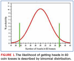
The Weibull distribution was invented by Waloddi Weibull in 1931. This invention fact was recounted by Dr. Robert Abernethy in his famous textbook on Weibull analysis: The New Weibull Handbook. This statement may not seem unusual, until we ponder that all common distributions in statistics were discovered, not invented. The three most common statistical distributions are the normal, poisson and binomial distributions. As an example of a discovered statistical distribution, let’s consider the binomial distribution. This distribution describes, among other things, the odds in flipping a coin. If you flip a fair coin 60 times, you are most likely to obtain 30 heads (H) and 30 tails (T), but getting 29 H and 31 T or 32 H and 28 T would not be all that uncommon. Mathematical analysis shows that the curve in Figure 1 results. If a coin flipping experiment is performed many times, this curve will faithfully predict the results. The curve is not invented; it is discovered from the deep theoretical underpinnings of the binomial distribution.
The fact that the Weibull distribution was invented suggests that Weibull selected it because it fit many types of failure data. He defined cumulative Weibull distribution as:
F(t) = 1 - e-(t/η)β
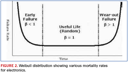
where eta is the characteristic life or the scale function, and beta is the slope, where as F(t) is the cumulative fraction of failures. Weibull proposed this function because for beta less than 1, F(t) describes “infant” mortality fails. In this situation, the failure rate is decreasing with time. For beta greater than 1, it describes “wear out” failures, where the failure rate is increasing with time. In electronics, we typically try to weed out infant mortality by using “burn in.” For beta equal to 1, the failure rate is constant. These three scenarios are shown in Figure 2. So typically, in electronics failure analysis, we are plotting failure data versus time to determine beta and eta, typically with software like Minitab.
Weibull himself was a curious character, and much of the available information on him is chronicled by Abernethy. For sure Weibull was a vigorous man. His second wife was almost 50 years his junior, and he fathered a daughter at about 80 years of age!
Ron Lasky, Ph.D., PE, is instructional professor, Thayer School of Engineering, Dartmouth College, and senior technologist, Indium (indium.com); ronlasky@aol.com.
Setting up the electrostatic discharge workstation.
Setting up an ESD workstation or area to reduce the risk of ESD in the workplace is simply a matter of understanding your processes and installing the necessary and proper ESD avoidance materials. However, simply installing ESD avoidance materials and items without understanding how they will impact the processes may cause misunderstanding and misuse. It is always best if ESD avoidance materials and items work seamlessly with your processes. This means that you can control electrostatic charge generation and charge accumulation and any subsequent discharges that are above your predetermined tolerance level without doing anything unusual.
The first consideration, as stated clearly in ANSI/ESD S20.20 (S20.20), is to understand the ESD sensitivity of the materials or components involved in your processes. Once you have settled on that level, the controls can be efficiently designed. The first rule in the design of an electrostatic protected area (EPA) is, if personnel are handling unprotected product (outside of protective containers or packages), establish a means of personnel grounding. Along with grounding people, some sort of protective work surface is generally needed upon which to place the sensitive product while performing the necessary operations.
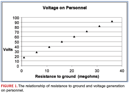
The design of the grounding system depends on your needs. A main consideration is whether personnel have to be mobile. If they require mobility, a floor and footwear system that provides a path to ground through the personnel is generally recommended. Today, a resistance to ground specification of <3.5 x 10⁷Ω (3MΩ) is considered optimum for most applications where >100V Human Body Model (HBM) parts are handled. It is also important to have an understanding about charge generation characteristics of the floor and footwear system. Make certain that the peak voltage generated by contact and separation of footwear from the floor does not exceed predetermined limits (generally >³100V measured on the person for most applications – see ANSI/ESD STM 97.2). The next release of S20.20 (expected late in 2012) will place more emphasis on the voltage on personnel and make the STM97.2 method the main test procedure for qualification of a floor and footwear system. If extremely sensitive products are processed, the resistance to ground level and the voltage generation level must be set lower. A rule of thumb in common use today is to reduce the resistance to ground level to <1 x 10⁷Ω (10MΩ) and the voltage level to <50V for extremely sensitive parts. Increased resistance to ground permits higher charge generation and accumulation (Figure 1).
If personnel are seated to do their work, a wrist strap type grounding system must be employed. The rationale is that seated personnel rarely have their feet in solid contact with the floor. Even if an ESD control floor and footwear system are in place, seated personnel have to use a wrist strap or a proven and documented equivalent type of grounding system to ensure consistent and
continuous grounding. The resistance to ground specification for a wrist strap grounding system is the same as stated above for a floor-footwear system: ≤35MΩ for a 100V HBM program and ≤10MΩ for more sensitive applications.
Verification that the grounding system is functioning correctly is of major importance. In general, the higher the risk or cost of failure, the more the grounding system must be checked. Most companies establish a minimum of one test per shift for personnel grounding. Many companies will require a retest each time a person returns to their workstation. In high-reliability or high-risk situations, continuous monitoring may be required. Once only required for military electronics, today many companies find it cheaper to use continuous monitoring, since it reduces test time and record-keeping. Personnel are taught to stop work when the wrist strap monitor sounds an alert, so that the problem can be fixed immediately.
Verification that the floor and footwear system is functioning according to specifications is usually done with less frequency than a wrist strap system. ESD control shoes are not prone to change as much as wrist straps, but do not get complacent. Shoe grounding straps can be installed incorrectly, so they should be checked each time they are put on to make sure they are working correctly.
Properly installed floors do not change much over time, but can get ruined in a heartbeat with improper maintenance. Putting the wrong wax on a conductive floor may make it look nice, but will no doubt alter the performance. Most companies require a retest of a floor after cleaning or maintenance to make sure the electrical properties are unchanged.
A work surface can be a tabletop, workbench, conveyor, machine surface or any other place that holds products during a process; thus, the mechanical and physical requirements for a work surface will vary with each application. In general, the main electrical requirement of an ESD protective work surface is to permit a charge to drain from conductive or dissipative items placed on that surface. How rapidly the charge drains depends on the resistance of the ESD protective work surface and the contact resistance between the surface and the item. If the item is a charged ESD susceptible part, care must be taken to avoid Charge Device Model (CDM) issues. However, proper handling of parts will reduce charge generation and charge accumulation on the part and thus reduce CDM issues at the same time. Many companies operate facilities with very conductive work surfaces (e.g., stainless steel benches) with no ESD issues.
Contact The ESD Association (esda.org); info@esda.org.
Glob tops enhance reliability of space-saving bare chip assemblies.
For many handheld consumer and industrial devices, strict area and height requirements preclude the use of traditional lead frame packaging, in which an IC chip is enclosed in a plastic package with external leads that are connected to the chip. Bare die mounting – also known as chip-on-board (COB) – has grown in popularity as a way to reduce the footprint of electronics in space-restricted devices. Bare chip components are typically mounted to a printed circuit board or substrate using die-attach adhesives, and then electrically connected to the board, substrate or directly to another chip through fine wires in a process known as wire bonding.
Because bare die and their connecting wires have no protective plastic package, they can easily become corroded by moisture or chemicals if not adequately protected. The chip and wires can crack or break with mechanical stress – even with routine handling during manufacturing and assembly. Encapsulating the die and wires in a protective shell is critical to ensuring long-term assembly reliability.
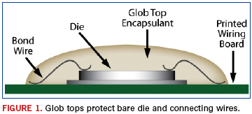
There are two main types of bare die encapsulation: transfer molding and liquid or glob top. Transfer molding involves placing a molding compound into an opening in a mold, forcing it into a cavity containing the component, and then curing the compound to form a plastic shell. Transfer molding exerts pressure on the die and wires and may cause wire sweep – the sideways movement of fine-pitched bonding wires – due to the flow characteristics of the molding compound. Wire sweep can result in short circuits or changes in electrical properties, such as mutual inductance. In glob top encapsulation, liquid encapsulant material is dispensed on top of a die and its wires, and then cured to form a protective barrier. Because it does not distort wires, glob top encapsulation is often preferred for applications involving fragile die or for larger chips, which typically have more connections consisting of finer wires with narrower spacing between wires than do smaller chips (Figure 1).
Thixotropic compounds. Glob top encapsulants are typically one- or two-part epoxies or UV-curable compounds that are specially formulated to be thixotropic – flowing easily in response to stress applied during application, but rapidly increasing in viscosity after placement. This change in viscosity permits the material to flow smoothly into narrow spaces without damaging delicate chips or wires, all while preventing the material from flowing beyond the target area. Once cured, glob tops protect die and wire bonds from contaminants and moisture, while providing sufficient mechanical support to prevent damage during handling and assembly.
Glob tops are designed to exhibit specific properties in order to protect and support electronic components. They are electrically insulative, resistant to moisture and chemicals, and are normally devoid of ionic impurities that may react with moisture and cause corrosion. To reduce the risk of moisture and contaminants penetrating the protective barrier and causing damage, glob tops should be free of solvents, which can lead to bubble formation, and should adhere well to all encapsulated surfaces. It is critical that glob tops exhibit minimal shrinkage and are low stress after cure, to minimize stress on the chip and its connecting wires. Glob tops are typically fairly rigid and provide sufficient mechanical strength to support fragile wires during handling.
The thermal characteristics of glob tops are carefully controlled to minimize thermal stress and help conduct heat away from the chip. Silica or alumina filler material is added to the base compound to reduce the coefficient of thermal expansion of the encapsulant, with thermally conductive alumina offering the added benefit of heat dissipation. CTE is a measure of how much the length of a material changes per degree change in temperature. If the CTEs of two adjoined materials are grossly mismatched, the materials will expand and contract at very different rates during temperature excursions, creating stress that may result in fractures or other failures. Because epoxies typically have CTE values that are much higher than those of silicon and gold, fillers are used to reduce the CTE and to minimize the thermal mismatch between the chip and substrate.
One-part epoxies are easy to use, require no mixing, offer unlimited working life, and cure within minutes upon application of heat. Although most one-part epoxies cure at 125°C, some newer grades cure at 80°C. Two-part epoxies require mixing, have a limited working life, and cure completely with little or no heat. At room temperature, two-part epoxies may take a few days to fully cure, but cures can be accelerated by applying small amounts of heat. UV-light-curable epoxy glob tops offer cure times that range from a few seconds to several minutes, depending on the coating thickness. For applications with very sensitive wire bonds that call for a softer material than epoxies, one- and two-part silicone glob tops can be used. These highly flexible silicones offer minimal stress, but are less resistant to moisture and chemicals than are epoxies.
Glob tops exhibit many of the same post-cure properties as conformal coatings, which are applied in a thin layer over an entire PCB and cured to form a protective barrier that conforms to all surfaces. Because glob tops form a thicker barrier, they offer more resilient protection than do conformal coatings, and are usually the preferred choice for bare chip devices.
Dispensing guidelines. The quality of the encapsulation is dependent on both the material and the dispensing system. To ensure long-term reliability, it is critical that the bare die and its connecting wires are thoroughly covered and that the encapsulant does not migrate beyond the target area. Precision dispensing is as important to successful encapsulation as the choice of encapsulant material. Two commonly used dispensing techniques are glob-topping and dam-and-fill.
In the glob-topping process, a precise volume of encapsulant is deposited from a reservoir through a needle valve onto the entire target area. If too little material is dispensed, the area may not be thoroughly covered. If too much is dispensed, a high-profile dome of encapsulant may result – possibly exceeding the assembly’s height requirements. Careful control over the dispensing process is necessary to prevent voids, which can lead to moisture diffusing into the target area. Material viscosity, reservoir pressure, and the space between the needle valve and the surface are among the controllable parameters that impact the process.
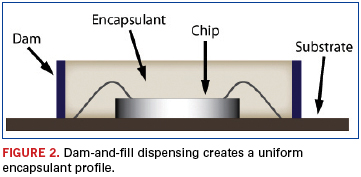
In dam-and-fill dispensing (Figure 2), a high viscosity material is deposited to form a dam around the area to be encapsulated, and then a lower viscosity material is dispensed at high speed within the dam. Because the dam limits the flow, this two-step process allows for a lower viscosity material to fill the dam – leading to a faster, more complete fill under and around the connecting wires and a more uniform encapsulation height compared to glob-top dispensing. Dam-and-fill dispensing is preferred for applications that have demanding chip height tolerances, such as low-profile smart cards.
For both glob-topping and dam-and-fill dispensing, a thermal heat source is often used to increase the material temperature during dispensing to achieve a lower viscosity and to enhance flow. The specific temperature of the encapsulant during dispensing is highly dependent on the type of material. To ensure smooth flow, the PCB or substrate is sometimes heated to 60° to 110°C prior to dispensing. Heat permits the encapsulant to flow completely around the wire bonds, reducing the risk of air pocket formation, which can lead to voids in the package.
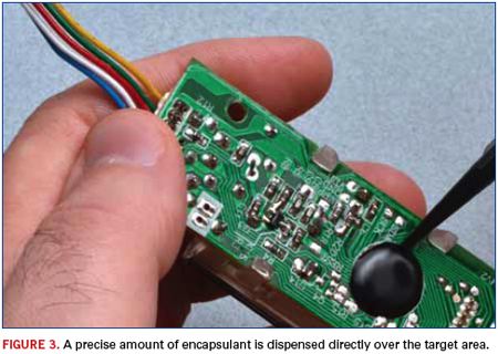
There are several types of glob top dispensing systems, varying in price and complexity. The simplest type is the syringe valve system, which consists of a needle that is attached to a syringe filled with the glob top material (Figure 3). Air pressure is applied to the syringe, causing the material to flow and dispense. The flow rate is dependent on both the viscosity of the material and the applied pressure.
An auger pump with a rotary positive displacement valve (RPDV) provides a more consistent flow than a syringe valve. The pump enables shear thinning: a decrease in viscosity in response to an increase in shear force. As material moves through the pump, the auger screw exerts a shear force, which lowers the viscosity during dispensing. Once the material exits the pump, viscosity increases with time, and the encapsulant remains within the target area. Both needle size and changes in motor speed affect flow rate and pressure drop at the encapsulant exit location. To maintain a consistent dispensing volume over time, a mass-calibration system can be used to measure flow rate and adjust dispensing speed.
Among the fastest and most accurate dispensing techniques is the true positive displacement pump (TPDP). This pump uses a motor-driven metal piston to displace an exact amount of material from a closed chamber, allowing for precision control over encapsulant flow. By moving the piston slowly, operators can ensure a consistent flow process.
To help ensure void-free encapsulation, manufacturers sometimes place their product under a vacuum or in a pressure cooker during or immediately after dispensing the glob top encapsulant. The dispense-in-vacuum technique accelerates material flow, drastically reducing the likelihood of voids within the glob top. Placing a product in a pressure cooker just after dispensing the glob top offers a dual benefit: The pressure collapses any voids, while the temperature accelerates the curing process.
Epoxy and UV-curable glob top encapsulants are specially formulated to exhibit specific physical properties during application and cure, while achieving desirable post-cure properties. They provide an economical, space-saving solution, offering environmental protection, mechanical support, and thermal dissipation for large chip-on-board devices.
Venkat Nandivada is manager of technical sales at Master Bond (masterbond.com); technical@masterbond.com.
Modifying small form-factor PCBs using preformed pads can save thousands in tooling costs.
Need to fix a PCB? Easy. Need to fix a substrate or interposer? Not easy.
A number of variables contribute to the level of difficulty, but the primary delta is the difference in pad and trace size. Repair kits are available for large form factor boards with their larger feature sizes, but smaller form factor boards (and features) are not as readily available.
For larger pads and traces on traditional PCB designs, suppliers offer repair kits containing various combinations of pads, traces and lands. Larger and wider pads can be fabricated with various techniques to yield copper and copper base metal solutions with and without enhanced solderable surfaces. Tighter aspect geometries (less than 150µm) prove more difficult than larger pitch (400µm and wider) geometries.
Traces are narrow; metallization is thinner, and it is possible that metal finishes might not suit solder profiles; for example, thick gold on small pads can lead to embrittled solder joints with small flip chip bumps. As a result of these smaller geometry requirements on small form-factor boards, fabrication techniques prove more difficult due to undercutting on etch solutions and any number of issues with laser-cutting (heat damage, inability to cut fine geometries, metal curling and subsequent plating issues) and flatness when stamping or punching.
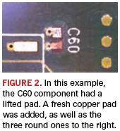
For small or standard form-factor PCBs, “modification,” not repair, can be required. Metal shielding, an extension to a power or ground plane, addition of a passive or active component, or any other modification are design changes that might need to be reviewed prior to investments in new die and boards. Removing failed devices can cause lifted pads, damaged traces, and corrupted metallization that require repair. Repair is a better solution than scrapping or ordering replacement boards. Both can be expensive, of course, and lead to delays, and in some cases do not yield acceptable results, resulting in scrap.
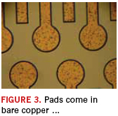
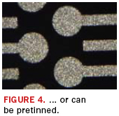
A new novel board repair kit includes fabricated traces and pads, which are then placed on the board (Figure 1). Custom shapes are available, as well as standard circular and round pad sizes of 150, 200, 250, and 300µm geometries (Figure 2). Pad sizes in sub 100µm geometry footprints with and without traces/tails can be fabricated as well. Base metals of copper can be plated with ENIG, gold, SAC, tin, and SnPb (Figures 3 and 4). Sidewalls have less than 5% taper, so tight geometries can be fabricated. (Spiral inductors have been fabricated with spaces less than 6µm on 10µm wide traces.)

In many cases, especially for high-frequency boards, modifying the board is less expensive than repairing it. In some cases, the pads have been mounted on boards and used as antennas.
In one instance, four modifications were performed on a series of buildup boards, saving the customer considerable time and expense. “We are very pleased in the ability to solder down the flip-chip substrates, and it allowed us to test modifications on the substrate at a speed that would be impossible through the normal substrate design cycle of ~1.5 months,” said Francisco Ledesma of nVidia. “The process allowed us to try several substrate modifications without incurring the large expense of redesigning the layout several times. In the end, this provided us fewer design iterations, less time and lower cost.” Given that tooling charges for buildup boards can cost up to $50,000 to $80,000, it is estimated the customer saved more than $200,000 in tooling costs alone.
Turn times are typically less than one week. Structures can be shipped on gel packs, inside vials, tape and reel, or in custom packages.
Terence Q. Collier is president of CVinc (covinc.com); tqcollier@covinc.com.
Why touch-up should be used sparingly, if at all, and other helpful hints.
We rework and repair printed circuit boards every day. From our experience, here are the 10 most common rework mistakes – and their solutions:
1. Mistake: Trying to fix what is not broken.
Fix: Do not rework a good solder joint that just “looks funny.” Know the IPC-A-610 workmanship standards and the class being inspected to. Do not try to fix a solder joint that passes those standards. Adding another heat cycle to make it look prettier is not good for long-term reliability.
2. Mistake: Excessive pressure or pressing down with the solder iron.
Fix: Use light pressure only. You cannot drive more heat in by pushing the tip into the pad. Doing so only increases the chance of lifting the pad or measling the board.
3. Mistake: Using a higher temperature to solder faster.
Fix: Cranking up the heat does not necessarily make the solder flow better. In fact, if you crank it too high, it will reduce the flow because the tip oxidizes too quickly, and the higher temperature burns off the flux too soon. The best way to get maximum flow and hole fill is to combine the right temperature (generally 700°-770°F) and dwell time (generally 2-5 sec.).
4. Mistake: Lack of proper ESD protection.
Fix: Maintaining the same electrical potential between the operator, work surface and ESDS device is critical. Simply wear a wrist strap and use an ESD table mat that is properly connected to a common point ground. What good is it to fix a defect perfectly but cause a latent ESD failure that will manifest itself in the field? Proper ESD protection is simple and inexpensive, so be sure to get grounded.
5. Mistake: Improper use of flux.
Fix: Before soldering, ensure appropriate flux is being used. This will eliminate oxidation, which harms solderability. It also will add wetting and improve your technique. Additionally, remove the flux with an appropriate cleaner to eliminate the possibility of dendritic growth.
6. Mistake: Improper tip size.
Fix: Select the largest tip that will not extend over the annular ring. It takes a few extra seconds to change the tip, but it pays off in better workmanship.
7. Mistake: Not cleaning and shocking the tip.
Fix: Every solder station should have a wet, sulfur-free sponge to clean, and be sure to thermal shock the tip immediately prior to soldering. This will help the solder flow, aid in heat transfer and prevent FOD.
8. Mistake: Not cleaning after rework or touchup.
Fix: Always clean the flux from hand-soldered PCBs, even if no-clean flux is used. No-clean flux only can be left on when it is fully cured. In hand soldering, unlike in the reflow oven, all the flux is not cured, so ionic contamination or dendrite growth will occur.
9. Mistake: Collateral damage.
Fix: With today’s densely packed PCBs, operators must be extra careful not to displace or reflow adjacent components. It even may be necessary to tape off adjacent components to protect them.
10. Mistake: Improper training.
Fix: Get the proper training for the job. Owning a solder station does not make you a rework technician. A one-week IPC-7711 class provides the skills to fix almost any PCB rework problem.
Bob Doetzer is president of Circuit Technology (circuittechnology.com); bob@circuittechnology.com.

Press Releases
- Zollner Puts a New Mechanics Building into Operation
- Changes in Incap’s Management Team: Incap updates its leadership model to support its growth strategy
- Niche Electronics Celebrates Completion of Florida Expansion
- Microscreen Names Nik Thomas Director, Expands Leadership Role Amid Continued Organizational Growth