

New systems are more robust, faster curing and require less energy than conventional chemistries.
With each passing day, use of silicone rubber is becoming more and more pervasive; products made from silicone are showing up in hospitals, cars, the kitchen and bath, even golf bags. Flexible bakeware and cooking utensils, fuel-resistant hoses and gaskets, airbags and touch pads, shampoos, skin care products and much more are all made possible with new silicone technologies. Dr. Fredrick S. Kipping, the father of silicone chemistry, could never have envisioned the plethora of uses into which his “sticky mess” has grown. From the earliest days of commercialization, silicones have always been selected for any high-performance specialty application that requires durability and outstanding physical properties.
Silicone chemistry is a unique combination: neither purely organic (i.e., carbon-based) nor purely inorganic (i.e., silicon-based), but a molecular-level hybrid of both. The nature of the Si-O bond in the polymer backbone creates low rotation barriers and large bond energies. This inorganic polysiloxane backbone provides the foundation for building materials with superior thermal properties, environmental resistance and flexibility, even at temperatures below -70oC. The methyl groups pendant to the Si-O-Si chain provide for low surface energies, and the low rotation barrier along the backbone permits the polymer to freely orient these groups to the exposed surfaces. The hydrophobic character and soft-touch feel of silicone-based materials is a direct result of this combination.
Silicone elastomers are used as sealants, adhesives and coatings, where they are fluid-applied and cured in place, but may be also molded into a multitude of shapes and used to produce functional products in a range of applications. There are two predominate cure types: condensation-cure and addition-cure. Condensation cure products may be either single-component or dual-component, generally use tin catalysts, require moisture to react and liberate alcohol or other monomers as byproducts during cure. Addition cure materials may also be either single-component or dual-component, are either free radical cured or rely on precious metal catalysts, but perhaps the biggest distinction is that there are no byproducts generated during cure.
Certainly nearly every homeowner is familiar with single-component, condensation cure silicones, perhaps even using some to caulk the bathtub or kitchen sink: the familiar smell of vinegar as acetic acid is liberated during the condensation reaction. Single component, moisture cure, RTV silicones (room temperature vulcanizing) are valued for their ease of use, adhesion, physical properties and environmental resistance. The products are manufactured under dry conditions and stored in moisture-proof packaging. Once applied, the material draws humidity from the atmosphere and begins to cure. The cure proceeds from the outside inward, with the rate of cure determined by the amount of catalyst in the formula, but more important, by the amount of moisture available. The byproduct liberated is dependent on the leaving group of the cross-linker used in each specific formulation (Figure 1).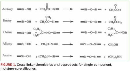
Within electronics, moisture-cure RTVs are often employed as staking compounds, where vibration dampening and stress relaxation are important. These types of staking compounds are most often shear-thinning pastes that, once applied, resist flow and may be used to build up a protective barrier around sensitive components. When fully cured, these materials become relatively soft (i.e., Shore A 25-45), durable, low modulus rubbers. Many silicone conformal coatings are also based on this type of chemistry. The advantages are ease of application, solvent-free formulations and environmental resistance of the cured films. Silicone conformal coatings are most widely used in high-temperature environments, making them the primary choice for under-the-hood automotive applications. However, because moisture from the atmosphere is needed to catalyze the cure single-component, RTVs must only be applied in thin cross-sections, typically less than 0.5", and the assembly must be racked overnight to permit slower cure speeds.
Less familiar, but no less functional, are the dual-component condensation cured silicones where the cross linker and catalyst are contained in separate packages that must be mixed prior to application. Here, the moisture is an integral part of one component, making these formulas much less sensitive to environmental conditions. Also, because the reaction is not dependent on the transport of moisture from the atmosphere, these materials are able to cure in thicker cross-sections. However, a byproduct is still generated during cure, so shrinkage is relatively high.
High consistency silicone rubber (HCR) compounds may be processed by injection molding, compression molding, and extrusion or calendaring. These are the original single-component, addition cure rubbers: typically, ready-to-use blends of silicone rubber with fillers, modifiers and vulcanizing agents that are heat-cured to form elastomeric components. The vulcanizing agents are generally peroxides that break down with heat, generating free radicals that initiate the cross-linking reactions.
Liquid silicone rubbers (LSR) are also based on addition cure chemistry. Generally, two-part pumpable materials that must be mixed and often heat-cured to form elastomers are suited for intricate designs manufactured in large, automated quantities. LSRs rely on precious metal catalysts, usually platinum, to promote cross linking. As with the condensation cure, two-component formulations, the catalyst and cross linker are contained in separate packages that must be mixed prior to application. LSRs and fully-fluorinated LSRs currently represent the fastest growing branches of the silicone family tree.
Platinum-catalyzed, addition-cure silicones may be formulated with an extremely wide range of physical properties and cure characteristics, which makes these materials very popular. One of the most exciting developments is the introduction of low viscosity, optically clear potting and encapsulating compounds. LEDs, photovoltaic subassemblies and other light-sensitive devices require radiation-resistant, non-yellowing encapsulants for protection and improved light transmission. For radiation energy to initiate any chemical changes, causing a breakdown in properties and yellowing, the polymer molecules must first absorb it. Because of the absence of any double-bonds or other ultraviolet (UV) light-absorbing groups polydimethyl siloxane-based, addition-cured silicones absorb very little ultraviolet radiation in the 300-400nm region. As mentioned, the bond strength of silicon-oxygen linkages in the polymer chain is exceptionally high, which prevents oxidation and loss of properties.
In the past, there were concerns that silicone oil migration or bleed out would contaminate sensitive electronic components. Early formulations used silicone polymers that were not stripped of low molecular weight contaminants, and electronic devices relied heavily on mechanical switches. These low molecular weight oligomers could volatize and condense on switches; because silicones are excellent dielectric materials, this could cause poor contact and device failure. Today, silicone polymers go through a much more extensive stripping process to remove and control contaminants. Device design also has improved, so the technology is not as susceptible to any potential contamination.
Heat cure, moisture cure, mixing, ovens: All are fine and effective means for curing products to generate pieces and parts for a great many applications. The real interest and some of the fascinating performance advances are in the field of UV-curing silicone rubbers, with the advantages of speed, ease of application and energy efficiencies associated with traditional UV curing to produce elastomeric materials with all of the performance enhancements of silicone.
The concept of UV curing silicones is not new. Acrylic end-capped, free-radical cure silicones were first commercialized in the early 80s. While they are technically UV cure, these dual-cure systems rely quite heavily on the traditional moisture reaction to affect full cure. The acrylated-silicones are sensitive to oxygen inhibition, require fairly significant energy input to initiate the reaction, and need prolonged exposures to complete the cure. Perhaps because they are not so robust, these materials have not enjoyed the market success of hydrocarbon-based UV cure technologies.
The thiolene “click” reaction is very powerful chemistry. Click chemistry is not one specific reaction, but more of a concept or a philosophy introduced in 2001 by K. Barry Sharpless, Ph.D. of the Scripps Research Institute.1 By definition, click reactions are simple and robust. They use only readily available starting materials, require no solvent, or chemically benign solvents (e.g., water), and proceed to high conversions. Applying these concepts to polymerization reactions yields materials that are extremely dynamic. Thiolene chemistry is the reaction between thiol groups and vinyl functionality. If the molecules involved contain higher functionality (i.e., F(x) >/= 2), then the reaction will produce polymeric materials. The process is normally photoinitiated and proceeds via a very rapid step-growth mechanism; an idealized outline of the initiation – propagation – chain-transfer reactions is shown in Figure 2.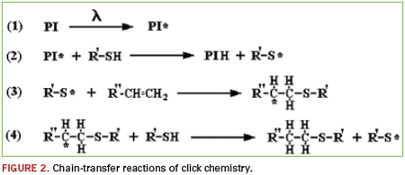
In addition to the polymerization reactions discussed earlier, the thiolene reaction may also be used as a cross-linking mechanism. High molecular weight, vinyl functional polymers may be cured with short-chain, or monomeric, multi-functional thiolene curing agents via the same photoinitiated reaction. It is essentially an addition reaction, so no byproducts are produced, and shrinkage is low. There are hundreds of vinyl and thiol combinations. Vinyl functional polydimethylsiloxanes are abundant and readily available, and there is a fairly wide selection of short-chain mercapto-functional polysiloxanes. This combination may be employed to produce UV-cured silicones.2,3 These systems were originally investigated as possible release agents for paper coatings.
This chemistry has been extended to include a secondary moisture reaction for curing in shadow areas and to further increase cure strength, adhesion and system dynamics.4 Clear materials based on this new system are much more robust and cure to greater depths with much lower energy requirements than conventional acrylated silicones. This translates to increased processing speeds and faster turnaround. Essential for protecting electronic circuitry and significantly extending the service life of printed circuit boards, conformal coatings are an integral component of the entire sub-assembly. Eliminating moisture and contamination is a key element for protecting sensitive electronics. Silicone conformal coatings provide an effective barrier, even under the most severe service conditions. Now UV-cured conformal coatings that offer all the enhanced performance characteristics of conventional silicone-based materials, but with higher processing speeds, are available.
Perhaps more important, these new UV-cure, silicone resins may be filled, which means pigmented and even electrically conductive UV-cure silicone products are now possible. Flexible and printed electronics (FPE) incorporate several new technologies and emerging processes and materials across a variety of applications. FPE may be twisted, bent or shaped without damage, enabling endless innovation and unlimited possibilities.
When an application requires performance, durability and physical properties, a silicone-based product is the superior choice. No other chemistry provides the environmental resistance and performance at thermal extremes. While it is true that silicones are critical for applications under the most severe and harsh conditions, it is also true that the enhanced adhesion, increased flexibility and UV and moisture resistance are important for many less-demanding applications.
References
1. H. C. Kolb, M. G. Finn and K. B. Sharpless, “Click Chemistry: Diverse Chemical Function from a Few Good Reactions,” Angewandte Chemie International Edition 40 (11): 2004–2021, 2001.
2. Lee, et al., U.S. Patents Nos. 4,946,874 (1990) and 5,124,212 (1992), Dow Corning Corp.
3. Viventi, U.S. Patent No. 3,816,282 (1974), General Electric Co.
4. Chambers, et al., U.S. Patent No. 7,105,584 (2006), Novagard Solutions.
Brian Chambers is director of technology, Novagard Solutions (novagard.com); bchambers@novagard.net.
A prime defense contractor offers alternate methods for ferreting out bad parts.
The sale of and resulting use of counterfeit components is a growing problem in the electronics industry.1,2 Detection of these products is crucial for use avoidance and to identify vendors and sources. The most common and obvious means of detection are visual examination and electrical testing. Visual examination answers such questions as: Are the packages the correct size? Is the proper number of leads present, and is symbolization correct? Electrical testing verifies that a component performs to specification. X-ray imaging is also common and reveals features otherwise inaccessible short of destructive analyses.
This discussion points out alternate, less common methods for counterfeit detection. These are important, as often components that seemingly pass incoming inspections may still be counterfeit.3 Examples discussed highlight use of some of these methods and represent examples investigated by the Raytheon Failure Analysis Laboratory, McKinney, TX.
It must be stressed that during an investigation, a finding that suggests a part is counterfeit must be verified beyond the testing itself. For example, if a construction material is identified that is not the same as that on a verified genuine comparison part, the investigators must ensure that this is not accounted for by acceptable changes made by the manufacturer. This underscores that such investigations are often not as straightforward as they may seem.
Vibrational spectroscopies. Fourier Transform Infrared (FTIR) and Raman spectroscopies are very useful at determining material compositions. These methods are sensitive to molecular vibrations, indicating the types of molecular bonding present in samples under investigation. The spectra that result are often likened to “fingerprints” and, as such, can be used for materials verification and identification. These methods are well-known for analysis of suspect counterfeits and fakes, as applied to fields as diverse as pharmaceuticals to the art world.4
Possible uses of these techniques toward counterfeit electronics detection include verification that the correct materials are present on parts, or the detection of foreign materials used to alter parts. In the following example, a verified counterfeit is compared to a genuine part. This demonstrates how these methods helped in detection of the counterfeit.
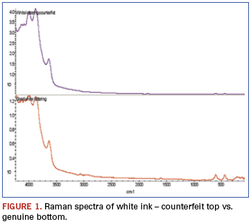
The package in question had white ink symbolization applied on one side and black ink on the other. The suspect part had correct markings per se; however, it was suspected to be counterfeit. Investigations of the applied inks helped verify this assumption.
In the Raman spectra (Figure 1), bands beyond 3500cm-1 result from alumina when analyzed using a 532nm laser. The two bands centered around 500cm-1 result from titanium dioxide. Both are used as white pigments. While each is present in the ink on both samples, the ratios are dramatically different.
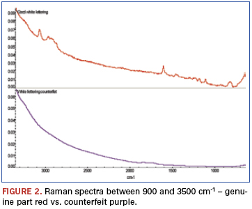
An additional finding (Figure 2) was made from analysis of weak bands between about 900 and 3500cm-1 of these spectra. The bands identified in this region show the genuine part ink to be epoxy-based, while similar bands are missing from the counterfeit part ink spectrum. FTIR was chosen to further investigate these samples (Figure 3). FTIR investigation revealed the base polymers were different: The genuine part was composed of an epoxy-based ink, while the counterfeit was composed of a urethane.
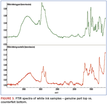
Analysis of the black symbolization using these same methods resulted in similar results: Both inks had the same pigment: carbon black; however, the base polymers were different.
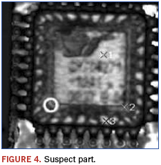
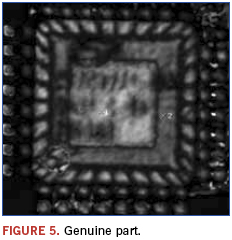
Scanning acoustic microscopy (SAM). Acoustic microscopy is a technique that uses sound waves as opposed to electromagnetic radiation for imaging purposes. It depends on the differences in the speeds which sound waves travel through different media; this is typically a function of material density. As such, it is capable of imaging internal device structure nondestructively via sound waves as they pass through various materials and interfaces between materials. One of the more common applications is detection of voiding within packages. (Sound propagation is much different between gasses and solids.)
In the following example, SAM was used as part of a multi-technique investigation that resulted in verification that a lot of parts was in fact counterfeit; the data were presented to the legitimate part manufacturer, after which verification was confirmed.
In this example, a lot of programmable grid array devices was suspect. This resulted from visual examination indicating questionable symbolization; poor quality markings and logo differences were noted. Known good devices were on hand and used for comparison purposes. Figures 4 and 5 show the recorded images.
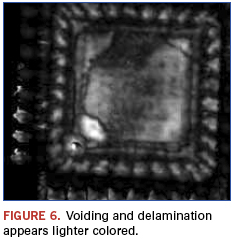
Immediately apparent from the images is that the die and die paddle sizes are different between the suspect and genuine part. Additionally, as shown in Figure 6, the suspect part appears to have possible voiding and delamination as revealed using a technique termed ”C–scan.”
Gas chromatography/mass spectrometry (GC/MS). Gas chromatography is a separatory method that can detect volatile components of a mixture as a function of time that compounds take to travel through the system. This alone is often used for identification of materials; however, this is not typically useful for analyses of unknowns, as residence times are not known. To remedy this problem, GC systems are commonly coupled to MS detectors. This permits determination of molecular identity as a function of the mass of the molecules, and fragments thereof, under investigation. As was the case with FTIR and Raman methods, databases of tens of thousands and even hundreds of thousands of compounds are available for spectral matching and materials identification.
GC/MS is a much nuanced technique, and a multitude of sampling methods are available; these are applied as the samples dictate. The following example will focus on one of the less commonly used techniques, namely “pyrolysis.”5
Pyrolysis refers to the thermal decomposition of large molecules, for example polymers, into smaller fragments by rapid heating under inert atmospheric conditions. This method typically creates a multitude of small volatile molecules readily analyzed using GC methods. The “chromatograms,” sometimes called “programs,” typically contain hundreds or even thousands of peaks. (Each peak represents the detection of a unique compound in the mixture.) These chromatograms can be thought of as fingerprints, often with hundreds of points of reference. As such, this is a very powerful technique to determine if two materials are in fact the same.6 This is important, as many times techniques such as FTIR may indicate that two materials are of the same class, but cannot identify slight compositional differences such as variation in polymer additives between samples. While in the strictest sense MS detection is not necessary, it greatly helps interpreting the often complex data that result.
In the following example, the epoxy encapsulation of a suspect device is compared to a known good device. Suspicions were raised as the devices of a newly received lot had a glossier appearance than an older known good lot (Figure 7). Other analysis techniques could find no differences, and pyrolysis was chosen as the ultimate arbiter.
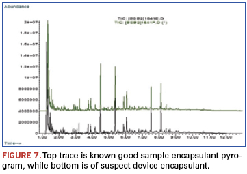
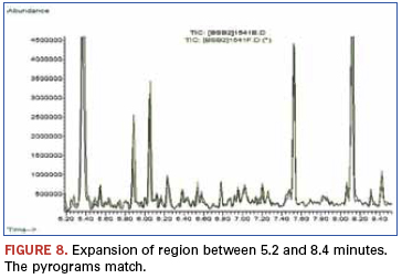
A quick visual examination reveals no noticeable differences between chromatograms. This is further displayed in Figure 8. These data demonstrated that while superficial appearance differences were noted between a suspect part and a known genuine part, the materials used to encapsulate the device were in fact identical. Performance testing also revealed no differences, and the suspect lot was accepted as legitimate.
A metallurgical example. While the following example is not outright counterfeit, it is a case of what is best termed a “misrepresentation” – an example of how counterfeit detection issues are sometimes blurred by shades of gray.
The chemical analysis technique applied in this case was inductively coupled plasma/atomic emission spectroscopy (ICP/AES). This elemental analysis
technique is typically sensitive to low part per billion (ppb) atomic concentrations. It is also very accurate and commonly used for metals and alloy analyses. This example highlights a common problem with metals analyses: Testing results may show the material to be of correct composition; however, the metals still fail via metallurgical defects associated with forging and processing.
In this example, receipt of sub-par balls used on a high-load mission-critical ball bearing is discussed. While this is not an example chosen from a circuit-card assembly perspective (this bearing was not part of a circuit card), parallels exist, as poor quality bearings, in our experience, represent a growing trend and affect mechanical devices that are mounted to printed circuit boards.7
After a bearing had seized during testing, a failure analysis investigation was initiated. As mentioned, compositional analysis using ICP/AES indicated the balls were within specifications. However, visual examination revealed that the balls were of questionable quality; obvious physical defects showed they did not meet the grade standard we believed to be purchasing.
All the cited examples are of balls from bearings that had seen no-to-extremely-limited use and represent forging defects and do not result from wear.
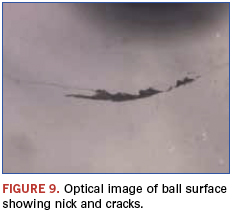
The cracks in this example (Figure 9) radiated out from the nick to cover approximately 33% of the ball diameter. Both defects were well beyond the ball grade thought to have been purchased. These features lead to reliability concerns and the possibility of catastrophic bearing failures.
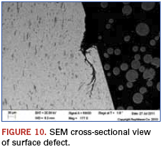
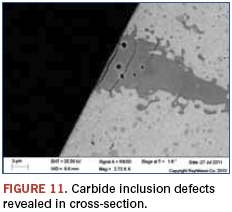
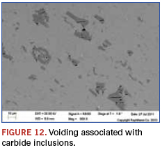
The cross-sectional view in Figure 10 shows that surface defects can radiate into the balls, and the potential for debris creation is heightened. Figures 11 and 12 show that the expected carbide inclusions contained a high degree of voiding and potential initiation sites of further defects when these occur at the surface. In the visually examined samples, about 20% of the balls had these large defects. Eddy current testing was used for screening large numbers of balls, and similar results were found.
While this example highlighted a chemical analysis technique that indicated the materials were within compositional specifications, they were in fact still not as represented. This stresses an important aspect of such analyses: A materials match, or even mismatch, alone is at times not sufficient for counterfeit
verification or even genuine part verification. Often, additional testing and inspection beyond initial investigatory methods are necessary.
The examples cited show a variety of techniques that can be employed during counterfeit detection. The methods cited are certainly not exhaustive, and a number of other techniques such as secondary ion mass spectrometry (SIMS), x-ray photoelectron spectroscopy (XPS), various chromatographic and mass spectroscopic methods, thermal analyses such as thermo gravimetric analysis (TGA) and differential scanning calorimetry (DSC), and a host of others are applicable to these ends.
These examples were chosen to highlight less common approaches to counterfeit detection and to illustrate the, at times, complicated nature of such materials investigations.
References
1. Mike Buetow, “No Counterfeits, No Excuses,” CIRCUITS ASSEMBLY, February 2012.
2. SAE International (Society of Automobile Engineers) has several commentaries at sae.org accessible by searching keyword “counterfeit.”
3. SAE is currently developing standards for use of such methods as part of the G19ATest Laboratories Standards Committee.
4. http://americanpharmaceuticalreview.com/ViewArticleaspx?Content-ID=210andWebExhibits,“Spectroscopy,”webexhibits.org/pigments/intro/spectroscopy.html.
5. Several good reviews are available on the web by simply searching the term GC/MS and variations thereof.
6. Many examples of uses of pyrolysis are available from CDS Analytical; cdsanalytical.com/prod_pyrolisis.html.
7. Karen Field, “Bogus Bearings Look More Real Than the Real Ones,” Electronics Weekly, April 10, 2007.
W. John Wolfgong, Ph.D., is a chemist, James Izzo a senior analyst and Mark Depriest a failure analyst at Raytheon Network Centric Systems (raytheon.com); wolfgong@raytheon.com.

Robust, cost-effective heat management must cater to differing applications and user requirements.
When it comes to addressing the thermal management demands of today’s advanced electronics devices, there is no “one size fits all” solution. Different applications and user preferences dictate the material type and performance to be selected. One thing is universal, however: effective thermal management – especially at the TIM2 level – is more critical than ever, as devices shrink in footprint and increase in functionality and, therefore, keep getting hotter. Robust, cost-effective heat management must also cater to differing applications and user requirements, and so a complete range of materials approaches for differing specifications is required.
Traditional thermal greases. Arguably, the most well-known thermal management materials are thermal greases. Well-liked for their good wetting ability, greases have historically been the material of choice for certain thermal applications. The lower processing costs of greases have also been part of the appeal, though they do have some performance challenges – such as “pump out” or migration -- over the long-term. While phase change liquids have to go through a step whereby they require a phase change transition to achieve desired performance, greases are functional as soon as they are applied and offer a viable alternative for manufacturers who want to avoid the extra processing requirements associated with phase change materials. Though phase change products generally offer better long-term reliability because they don’t pump out over time like greases, there are extra process steps required.
Thermal interface pads. There are applications and processes where pads are still an appropriate choice and are often used in place of traditional thermal grease. There are pads designed for applications that dictate extremely high reliability and are not bound by requirements for thermal performance. Examples where these materials have shown their effectiveness include base stations and power electronics. When electrical isolation is required, thermal interface pads that provide good thermal performance, cut-through resistance and dielectric strength should be utilized. Both of these interface pad types are excellent alternatives to thermal greases which, as mentioned, may suffer from reliability problems over time due to material migration.
Printable and dispensable phase change pastes. As an alternative to traditional phase change pads or films, liquid medium products that offer similar performance characteristics are enabling more process flexibility. The new materials, which are dispensable or printable, are phase change materials in liquid form that offer many of the advantages of thermal greases in terms of usability and throughput without the challenges that are inherent with greases. Both formats are pastes when applied and, over time, the materials dry and form a phase change pad. The reliability and performance of the materials are consistent with film phase change materials but, because they are liquids, thickness can be adjusted depending on the requirement. Films come in a variety of thicknesses, but extremely thin films are difficult to manufacture and often do not release cleanly from the liner. As the liquid materials can be fully automated, throughput is improved and adaptable to current equipment, permitting manufacturers to use standard dispensing or screen printing systems.
Thermal adhesives. To address emerging requirements for device size and weight and improved processability, many thermal management experts are turning to thermal adhesives as their preferred TIM2 materials. Not only do these products deliver the thermal performance required but, because of the permanent bond these materials provide, they eliminate the need for fastening devices such as screws and clips. Thermal adhesives in both paste and film formats enable manufacturing flexibility while facilitating the manufacture of smaller, lighter products. When thermal specialists want the advantages of an adhesive but require consistent thicknesses, the ability to bond large devices with complex patterns, and minimized voids, adhesive films are the obvious solution.
Clearly, there are no shortage of effective, application-specific thermal solutions from which to choose and each should be carefully evaluated in terms of cost, value, processability, ease-of-use and, of course, performance to specified requirements. I can say with relative certainty that we won’t see devices getting any bigger, making effective thermal management a huge factor in the reliability of next-generation devices.
Jie Bai is a chemist at Henkel Electronics Group (henkel.com); jie.bai@us.henkel.com.
Key aspects of ATE platform boards and how an IPC test panel design is used to qualify suppliers.
ATE platform boards are simply defined as interfaces used between a semiconductor device and an electrical tester. They include necessary circuitry for device testing and can also dock to a robotic handler for running high-volume production. Handler applications vary, generally manipulating either a semiconductor wafer (probe test) or an IC device package (final test).
Development stages of an ATE board include design, fabrication and assembly. The challenges and significant characteristics of making ATE boards put them into a distinctive category in PCB manufacturing. Some common considerations of ATE board fabrication include:
Via aspect ratio. Typical ATE board thickness requirements range from 0.125" to 0.250" (3.175 to 6.35mm). This board thickness is used primarily for mechanical stiffness. High layer counts are necessary for some test solutions, which results in a large board thickness in addition. The number of layers within an ATE board can be greater than 40.
The substantial thickness of an ATE board leads to electrical interconnect vias having a high aspect ratio. (Aspect ratio is defined as a via’s drill depth over its drill diameter.) As via aspect ratio increases, it becomes more difficult to achieve adequate copper thickness plated along the hole wall, especially at the barrel center.
Sequential lamination. Many PCBs are manufactured with only one lamination step (or press-cycle) to fuse all its layers together. Sequential lamination involves creating two or more multilayer boards first and subsequently pressing those together to form a single board.
Complex builds may require additional lamination cycles and might also use microvia buildup layers. This can lead to a particular board section undergoing two to five cycles in the press. Multiple lamination cycles are common for ATE boards. Reasons this is incorporated include aspect-ratio reduction, limited drill-bit flute lengths, and microvia buildup layers.
Multiple lamination cycles can cause a board to be more susceptible to delamination. Board delamination may not be apparent until after a component assembly reflow cycle or perhaps upon inspection after failure in the field.
Registration. Registration is loosely described here as the vertical alignment of PCB features on different layers. It is a critical aspect for attaining layer-to-layer electrical interconnects. Misregistration occurs during the PCB build process for numerous reasons. High layer counts, multiple lamination cycles, small PCB features, and errors compensating for material movement (that occurs during lamination) all contribute to the likelihood of registration failure.
While often viewed as a consideration for achieving a desired electrical interconnect, registration can also be thought of as an amount of drill-to-copper clearance necessary to maintain a desired electrical isolation. Drill wander is a separate issue, but its net effect results as a misregistration problem as well.
Multiple PCB features and technologies. ATE board designs can require multiple PCB features, feature sizes and process technologies. In that case, a fabricator must be capable and proficient with all. Specific technology requirements might include laser microvias, blind and buried vias, fine lines and spaces, backdrill through-holes, vias plated shut, partial-depth via plugging, selective NiAu finish, and very high layer counts. Other ATE board requirements can also involve atypically low tolerances for controlled impedance, positional accuracy, bow and twist, and relative copper feature height.
Resilience to mechanical and thermal stresses. Electrical interface to ATE boards is generally accomplished using spring-loaded pogo pins, which can number in the thousands on a given board, exerting a minimum of 25g of force per pogo pin. Pogo pin forces occur at both the electrical tester interface and the interface to the device(s) under test.
Docking to a robotic handler can also exert substantial forces on an ATE board. All these mechanical forces are typically dealt with using a combination of board thickness, metal stiffeners, and support plates.
Of even greater concern are the temperatures at which an ATE board might need to be subjected. Semiconductor device testing can have temperature requirements in the -50°C to 200°C range. A PCB expands in all directions as its temperature increases. Particularly stressful on an ATE board is thermal expansion in the z-axis, which can lead to via failure and board delamination.
In addition to the manufacturing challenges described, other characteristics of ATE boards contribute to their overall nature and drive further considerations. Factors including low quantities, long manufacturing times, and high cost and criticality not only impact board fabrication, but also affect decisions related to parts kitting, component assembly, post-assembly testing and end-user planning.
Evaluating ATE Board Fabricators
Because of the manufacturing challenges and critical nature of ATE boards, a non-subjective, quantitative approach is necessary when considering a fabricator’s capabilities, process quality and product reliability. A supplier site audit is not adequate, regardless of onsite equipment or plant cleanliness. Qualification practices based on examining sample coupons or accepting functional boards for evaluation have considerable limitations. Sole use of such methods invites risk to the semiconductor device manufacturer when qualifying an ATE board supplier as a link within this supply chain.
These quantitative measures described need to be obtained using a test vehicle that closely represents the end-product.1 In doing so, most manufacturing processes typically applied need to be included, even if more expensive, time-consuming and challenging. Statistical significance is important for reducing risk. Not many years ago, a race among PCB fabricators began in order to boast the highest aspect ratio through-hole via. Very high aspect-ratio claims made their way onto capability lists within manufacturer websites. The fact that a very high aspect ratio via is able to be produced does not indicate anything about its physical properties, predicted yields, manufacturing repeatability, and reliability under stress. As that became apparent to end-users, most fabricators have since removed statements of 30:1, 40:1, and even 50:1 aspect ratio capabilities.
Beginning in 2006, we adopted the use of standardized test panels to quantify capability, process quality and product reliability of existing and potential ATE board suppliers. The test panel design was selected to align with typical ATE board requirements. It is a 24-layer, multi-lamination build using an 18" x 24" (457.2 x 609.6mm) panel. It incorporates six via types, each built using two different drill diameters: through-hole, back drill through-hole, blind mechanical, buried mechanical, one-layer deep microvia, and two-layer deep microvia.
Test panels also include four plated-layer trace widths ranging from 0.003"-0.006" with three spacings of 0.004"-0.006." Four non-plated trace widths range from 0.002"-0.005" with three spacings of 0.003"-0.005." Controlled impedance is evaluated for 50Ω single-ended lines and 100Ω differential pairs on surface microstrip, embedded microstrip, and stripline. Coupons testing soldermask registration and conductive anodic filament are also utilized.
A test panel submission consists of 15 test panels manufactured in three equally-sized lots with no less than one week between the start of each lot. Requirements to achieve ATE board alignment include a target thickness of 0.187" (4.75mm), electroplated NiAu surface finish, and typically specified laminate materials. All manufacturing processes must reside within the facility producing the test panels. Disclosure is required if any outsourcing is used. Supplier results include quantifications in terms of defect densities as defects per million vias (DPMV) and defects per million inches (DPMI), percent registration yields, process variations as coefficient of variation (COV), capability potential (CP) and capability performance (Cpk), thermal cycles to 10% resistance change / open circuit, and hours to conductive anodic filament (CAF) failure.
Table 1 highlights the number of features both on this test panel design and the full submission quantity. 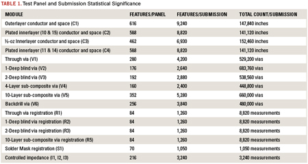
Suppliers are expected to complete the 15-panel set in about three months. Third-party testing takes one to two months to complete.
Latest Test Panel Study Results
Some notable observations from our supplier’s most recent test submissions include the following:
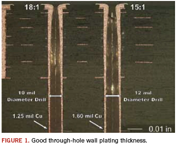
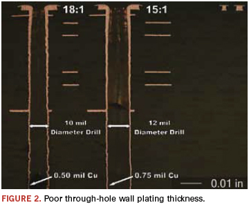
Via daisy-chain defects indicate 0.010" diameter, 18:1 aspect ratio through-hole vias continue to prove to be challenging for some suppliers.2 We found 0.012" diameter, 15:1 aspect ratio through-hole defects are better by a factor of at least three times, but results vary significantly among suppliers. Test panel cross-section photos revealed inadequate hole wall copper plating for both 18:1 and 15:1 aspect ratio through-holes in some cases. Figures 1 and 2 are test panel cross-section examples of good and poor through-hole copper thickness.
Test panels place registration coupons at each corner and amid the central area. Through-hole registration results are provided in terms of percent yields within an allowed radial distance outside a 0.012" drill diameter. Radial distances in this case measure from 0.003" to 0.008" given in 0.001" increments. Test data expectedly show that results are significantly better at the center area of the panel. It may be desirable to consider central panel registration results vs. panel corner results separately, especially in cases when boards are fabricated far from the corners. Combining test results from all areas, the greatest supplier results range for 0.012" through-hole vias was at the 0.006" radial distance.
Thermal cycle testing is performed similarly on all via structures used in the panel design. After test coupons are subjected to six passes of a 260°C assembly simulation reflow profile, they are placed in an air-driven temperature cycling chamber that attains extremes between -40°C and 145°C.3 Next, 4-wire resistance measurements are taken across via daisy-chain structures during cycling. Specifically noted is the number of cycles until 10% resistance change and cycles to open circuit, defined as 20Ω or greater.
Test results show thermal cycle performance does not always correlate to defect density. A supplier may have good defect density results, but poor thermal cycling performance at the same time. Significant differences were demonstrated between the 18:1 and 15:1 aspect ratio vias. 15:1 aspect ratio through-holes attained at least two times the number of thermal cycles achieved by 18:1 aspect ratio vias.
Mechanical blind vias on this test panel are 10-layer, 0.008" and 0.010" drills with aspect ratios of 6:1 and 5:1, respectively. Mechanical buried vias are four-layer, 0.006" and 0.008" drills with aspect ratios of 3:1 and 2.5:1, respectively. All areas of blind and buried via testing, including defects per million vias, registration yields, coefficient of variation, and thermal cycling show significantly higher performance than the through-hole via test results from all suppliers.
Use of lower aspect ratio blind and buried vias combined with sequential lamination and lower through-hole aspect ratios is the preferred build method for ATE boards over the use of high aspect ratio through-hole vias and no sequential lamination cycles.4
One-layer deep microvias utilize 0.003" and 0.004" drills with aspect ratios of approximately 1:1 and 0.75:1, respectively. Two-layer deep microvias utilize 0.007" and 0.008" drills with aspect ratios of approximately 0.85:1 and 0.75:1, respectively. One-layer deep, 0.003" laser drill defect densities continue to be at least two times higher than the 0.004" drill. Supplier results range widely among both drill diameters.
Both two-layer deep microvia drill diameters have significantly better defect densities than the one-layer deep microvias, but supplier ranges still vary widely. There appears a correlation of better results when in-house laser drill is performed vs. outsourced laser drill. Outsourced laser drill is demonstrated to have acceptable results, but considerations in regard to where post-processing and plating is handled should be made, especially if buildup microvia layers are used.
Laser microvia thermal cycling results demonstrate much higher performance than through-hole vias, achieving similar results as the 10-layer mechanical blind vias.
Conductor and space test results are provided for three different layer-types: plated outer layer, plated innerlayer and non-plated 0.5 oz. innerlayer. Plated outer-layers have a surface finish of electroplated NiAu specified at a minimum 200µin nickel underneath 5-15µin gold with Knoop hardness from 130-200. Plated innerlayers are a result of the sequential lamination build in this case and do not have a surface finish.
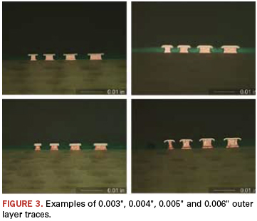
A conductor defect is simply a measurement of an open, and similarly a space defect is measurement of an adjacent short. Conductor defect densities on plated and non-plated inner-layers tended to be acceptably low, with a few supplier excursions seen on the smallest respective widths. Result ranges were observed to be much greater on the outer-layer conductor defects, especially with the smallest 0.003" trace width. Figure 3 shows four different supplier examples of the outer layer 0.003", 0.004", 0.005", and 0.006" conductors. Notably, significant differences are seen among all four examples in terms of copper trace etch factor, NiAu thickness, and length and shape of NiAu overhang.
More commonly encountered in ATE board development are space defects, especially when fine pitches are involved, and the test data reflect this. High supplier result ranges are observed on all layer types, especially at the smallest widths tested. Among all suppliers, the highest space defects occur on the plated outer layers. While defects per million inches is substantially highest with the 0.004" spacing and incrementally decreases by whole factors at both 0.005" and 0.006" spacings, very large ranges within supplier results are found on all outer layer space widths. Outer layer space defects were observed on test panel cross-sections (Figure 4).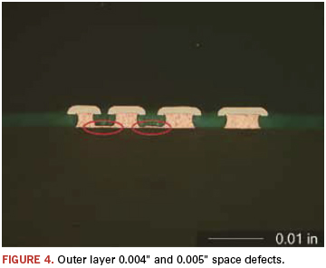
Managing Test Results Data
After receipt of supplier analysis reports, two applications of the data used are a scoring system and design for manufacturability rules. Developing a scoring system for supplier test panel results is advantageous for many reasons. The number of test results for each individual supplier is extensive. Such a system can be used to simplify data analysis and supplier comparisons. Different scoring weights can be allocated to areas according to the greatest emphases for ATE boards. Ranges for acceptable high and low ends of test results should also be included. Scores are used to identify weak areas and promote competition among suppliers without revealing one’s specific test results to another. Board fabricators can be told non-subjectively where they placed among the supplier base.
Allocating Weights
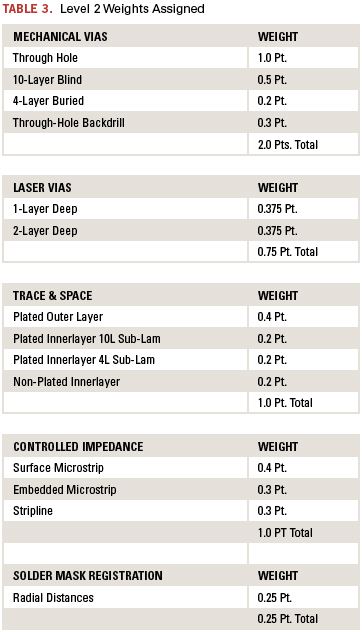
Level 1: The scoring system developed here is based on a 0 to 5 point overall scale. Many different test panel features, feature sizes, and test types require approaching the results on different levels. Level 1 represents the five highest test areas examined on this panel design: mechanical vias, laser vias, trace and space, controlled impedance and soldermask registration.
Based on the 5-point maximum, each area is allocated the weights shown in Table 2. Mechanically drilled vias are understood to be the weakest link in a high-performance ATE board and receive 40% of the total points. Trace and space and controlled impedance each get 20%, laser vias 15%, and soldermask registration 5%. Historically, soldermask registration capability has not strongly impacted ATE board development, but will likely become more important as component densities continue to increase.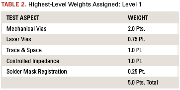
Level 2: Level 2 separates these five areas into their specific feature types. For example, mechanically-drilled vias comprise four different structures on this test panel design: through-holes, backdrill through-holes, 10-layer blind and 4-layer buried. Considerations for the amount of weight to apply to each feature type can include Difficulty to Produce, Frequency of Use, Susceptibility to Failure, and Supply Chain Availability. Table 3 is a breakdown of the five high-level test areas in terms of their feature types and shows the allocated weights assigned to each.
Level 3: Level 3 is the final level and involves specific test panel results. Feature types are further separated in Level 3 by two factors: Type of Test Performed and Feature Size. Six test types are considered for the through-hole vias: defects per million vias, registration, coefficient of variation, thermal cycles to 10% resistance change, thermal cycles to open circuit, and hours to CAF failure.
Considering the two through-hole drill sizes used, 0.010" and 0.012", 18 total test results are applied here for the through-hole feature type. Table 4 is an example of the Level 3 weights assigned for the through-hole via feature type. As with Level 1 and Level 2, weight allocations for specific test types and feature sizes can be based on several factors. In this example, the test types of defect density and registration are each allocated 30% of the total weight, thermal cycling 25%, process variation 10%, and CAF 5%.
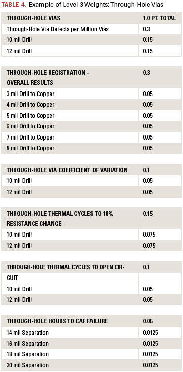
All different feature sizes have their allocated weights split evenly in this example, but that does not have to be the case. Emphasis may be placed on feature sizes more difficult to produce or perhaps feature sizes most commonly used.
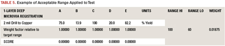
After weights are assigned to all individual tests, acceptable test result ranges are indicated and used to determine the supplier’s score on a specific test. A supplier’s result is compared against the acceptable range, and then a weight factor is determined. The weight factor is based on where the test result falls within the acceptable range.
Table 5 is an example of the 0.002" radial distance microvia registration for the one-layer deep feature. Here, five supplier test results are shown as A-E. The allocated weight for this test is 0.01875 points, and the specified acceptable range is 60% to 100% yield. In this case, the target is a maximum 100% yield. If a supplier achieves the target result or better, the entirety of the allocated weight is awarded. If the test result is at the farthest end of the specified range or worse, the supplier receives no score. When the result falls somewhere within the acceptable range, the supplier receives a percentage of the allocated weight determined by position within the range. In the example, a test result of 70% yield would earn 0.25 times the allocated weight; 80% yield would earn half, and 90% yield would earn 0.75 times the allocated weight.
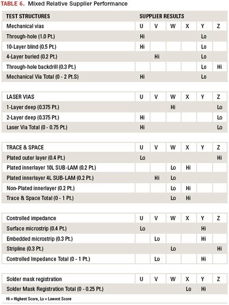
This scoring system is applied to a total of 212 test results for each supplier. Table 6 depicts highest and lowest scores achieved at Level 2 for six suppliers using color coding. Ranges between high and low scores are appreciable in all cases. The table demonstrates that no single supplier exceeds nor fails in all test aspects.
ATE Board DfM
Supplier test results can also be used as the basis for a DfM rule-set. When a multi-supplier strategy is incorporated, test results can certainly be used to determine recommended suppliers based on specific board build requirements. DfM rules should be implemented globally however. This ensures board designs are not limited to single-source manufacturability or perhaps a very limited number of suppliers. Whenever possible, the same aspect should apply such that novel, single-source technology capabilities are avoided if at all possible. DfM minimum and maximum constraints are used to establish quantified limits for improving fabrication yields. Whenever a design allows, absolute minimums and maximums should always be avoided and the number of their occurrences limited.
Mechanically drilled vias with high aspect ratios. As noted earlier, mechanically drilled vias with high aspect ratios have implications that go well beyond a supplier’s ability to merely produce them. This is considered to be the most critical DfM rule to be specified for ATE boards.5 Prohibition of techniques such as flip-drilling, used to attain very high aspect ratio vias, might also be considered. Regardless of how well a supplier can demonstrate the ability of such a process, the result is still a very high aspect ratio via requiring sufficient plating thickness.
Maximum laser drill microvia aspect ratio. Most suppliers specify a capability range between 0.7:1 and 1:1, with 1:1 commonly identified as “engineering level”.
Prohibit mechanical depth drilling for plated vias. The technique of creating blind vias without drilling entirely through a board has proven to yield very poor results in terms of defect density, process variation, and thermal cycling.
Mechanical drill hole wall to hole wall spacing. Drill wander, material properties, wicking, and susceptibility to CAF failure are some considerations in determining this specification.
Mechanical drill hole wall to copper feature spacing. This specification should vary depending on the depth of drilling involved. Test panel registration results provide a good basis for this.
Laser drill hole wall to copper feature spacing. Test results indicate a significantly smaller spacing is feasible among most suppliers than with minimum mechanical drill hole wall to copper feature spacing.
Copper feature to copper feature spacing. Fabricators may indicate this capability as a general minimum to be applied within an entire board, but supplier test results indicate consideration may be necessary for different cases of plated outer layer, plated innerlayer, and non-plated innerlayer.
Supplier Improvement Trends
After test panel data is received, supplier debriefs completed, and improvement plans are communicated, a common question is, Are the board fabrication suppliers getting better? Charts of average defect density trends for through-hole, blind, buried, and laser microvias all indicate supplier improvements. The following graphs represent our specific supplier test panel submissions. It should be noted they are not a representation of the entire PCQR2 database and all suppliers that participated within it.
Figure 5 shows that average supplier 18:1 aspect ratio through-hole DpMV has decreased since 2006 from a high of 3,009 to 1,234 from the latest test submissions. Average 15:1 aspect ratio through-hole DpMV ranged from highs of 643 and 708 in 2006 and 2008, respectively, to lows of 375 and 402 DpMV in 2009 and 2010, respectively.
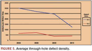
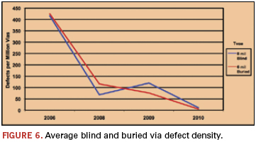
Figure 6 shows 10-layer, 0.008" blind vias had an average supplier defect density of 416 DpMV in 2006. This decreased to 11 DpMV by 2010. For four-layer PCBs with 0.006” buried vias, the average supplier defect density was 425 DpMV in 2006, decreasing to 5 DpMV by 2010.
Finally, 0.003", one-layer deep microvia DpMV fell from a supplier average peak of 2,882 in 2008 to 867 DpMV in 2010 (Figure 7). And 0.004", one-layer deep microvia DpMV fell from an average peak of 1,512 in 2008 to 395 in 2010.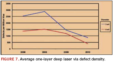
Conclusions
Benchmarking and qualifying PCB fabricators for semiconductor test boards requires a quantitative, statistically significant approach that otherwise invites unacceptable risk. Standardized test panels provide a sound basis for engaging with the supplier base and participating in continuous improvement plans. Over time, test panel results objectively demonstrate if suppliers are attaining agreed-upon goals. Since the test panels are close representations of the end-product, it is reasonable that measured process capability, quality and reliability improvements directly impact the fabrication of our ATE platform boards, contributing to maximum entitlement of semiconductor device manufacturing.
Acknowledgments
The author would like to acknowledge the support of Texas Instruments in this ongoing effort, and thank you to Mike Korson in particular. Thanks also to Norm Armendariz, John Hite, Pete Profilet, Martin Gao, Stan Ferrell, Jim Oborny and Marc Mydill. The author would like to acknowledge and thank the support of David Wolf and Tim Estes of Conductor Analysis Technologies. Special thanks to the IPC PCQR2 Database D-36 Subcommittee and all Texas Instruments’ ATE platform board fabricators.
References
1. D.L. Wolf, “Via Reliability – A Holistic Process Approach,” SMTA International, October 2009.
2. Bill Mack, “Benchmarking Printed Circuit Board Fabrication Suppliers Using IPC’s PCQR2 Database,” Burn-in & Test Socket Workshop Proceedings, March 2007.
3. IPC-9151C, “Printed Board Process Capability, Quality, and Relative Reliability (PCQR2) Benchmark Test Standard and Database,” May 2010.
4. Kevin T. Knadle and Virendra R. Jadhav, “Proof is in the PTH – Assuring Via Reliability from Chip Carriers to Thick Printed Wiring Boards,” Electronic Components and Technology Conference, June 2005.
5. Kevin Knadle, “Reliability and Failure Mechanisms of Laminate Substrates in a Pb-free World,” IPC Apex Expo, March 2009.
Ed.: This paper was first presented at SMTA International in October 2011 and is reprinted here with permission of the author.
William J. Mack is test hardware development engineer at Texas Instruments Inc. (ti.com); bigm@ti.com.
Process validation trumps inspection in the new Directive.
Directive 2011/65/EU (Restriction of Hazardous Substances – RoHS2) became European law on July 21, 2011. In summary, the law does not introduce new banned substances, but does require manufacturers to follow specific obligations in Module A of decision 768/2008/EC, with a focus on technical documentation and product checks. The module emphasizes requirements that “the manufacturer shall take all measures necessary so that the manufacturing process and its monitoring ensure compliance of the manufactured products.”
With the latest directive, RoHS is becoming more focused on validation of process, rather than inspection of results. Here, we detail the methodology of developing a compliance system to address the electronics manufacturer’s obligations.
Technical documentation. The technical documentation package, as defined in Module A, must contain at least a general description of the product, design and manufacturing drawings of components and subassemblies, and describe the operation of the product. Also noted in the module is a list of the harmonized standards that have been published in the official journal of the European Union, results of calculations, examinations carried out, and test reports.
Test reports can be interpreted many different ways and include various formats and information. The reports should include how the product was determined to be compliant during design and introduction to manufacturing; what controls are deployed to continuously mitigate the risk of noncompliance; and ongoing verification of product compliance.
Test reports can be created to qualify the initial compliance of the product and to describe how the product will be continuously verified as compliant. Technical documentation is required to be retained and readily accessible if an EU member authority inquires about product compliance.
Compliance software packages and systems exist to gather the above technical documentation. These systems can be purchased from various third-parties that provide this service. Alternately, some organizations have created the process and systems internally. The goal of either system is to gather and store the documentation required by the legislation and have the information readily available.
The next two sections detail how product can be verified as compliant on an ongoing basis.
Production control. Production or manufacturing control within this article is defined as the controls in place to mitigate the risk of product becoming noncompliant to RoHS.
The foundation of production control is the upfront component and material analysis completed to ensure that the electronics components are RoHS compliant with all supplier tests and declarations on file. These declarations and supplier test reports are part of the technical documentation package as described above.
If the facility is building non-RoHS-compliant product or still using leaded solder, controls are required to eliminate the risk of cross-contamination. Part number strategies and visual management are the two main tools for risk mitigation. Signs, color codes, and special part number nomenclature all can be used to educate the workforce on the RoHS-compliant material. As noted by European Union compliance enforcement last year, several instances of noncompliant product found during surveillance audits were the result of cross-contamination (leaded and lead-free solder) within the production process. If the risk exists, an analysis is required to determine cross-contamination opportunities. Examples of specific actions may be to color code tooling and equipment in the hand solder and wave solder operations.
Visual management can also be used on manufacturing materials such as solder. Most lead-free solders are marked with a separate part number, but also have a green color on the containers or packaging. Special attention is required for the risk of cross-contamination of reused solder paste. If dual (lead and lead-free) solder pastes are used, and the opportunity for cross-contamination is high, secondary green containers for lead-free are a good way to separate reused solder paste. Another example of visual management: Some solder bar manufacturers use triangular shaped bars to designate RoHS-compliant solder.
Product checks. One way to check and verify the product is through auditing the manufacturing process. This audit can be a quality systems type process audit that verifies the production controls and technical documentation detailed above. The audit will verify compliance to the system in place. A second type of check is testing the product and process to verify compliance.
Different types of testing exist to verify RoHS compliance, varying in cost, destruction of product and time of testing method. All have advantages, although one testing type has the added benefit of being portable, which enhances the ability of an electronics manufacturer to verify equipment, products and materials in real-time during the production process. This testing type is XRF technology. XRF technology (x-ray fluorescence analysis) is nondestructive and portable (Figure 1). A second benefit of XRF is the testing time, typically 30 to 60 sec. 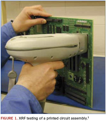
XRF testing can be the facility’s internal production control and technique to satisfy the process monitoring requirement of the directive. During electronics manufacturing, many variables and cross-contamination opportunities exist. XRF technology can verify that the various processes, equipment, tools and materials are compliant.
XRF testing during manufacturing. Many areas of the electronics manufacturing process can be verified with XRF. The testing intervals and areas to verify depend on product technology and risk of cross-contamination with leaded solder. The following manufacturing areas are potential XRF test points:
- Surface mount technology.
- Wave solder.
- Hand soldering.
- Final assembly.
The key is to verify the different process technologies (SMT, wave solder, etc.) and confirm compliance to the RoHS directive and banned substances.
The above testing method mirrors the compliance verification that several European Union enforcement authorities conduct during surveillance product audits. The results of the XRF product checks become an important part of the technical documentation package.
The RoHS2 Directive emphasizes product checks and technical documentation. We have described the compliance system methodology for which the technical documentation file can be provided to show due diligence. XRF verification has many benefits and mirrors the testing used by EU enforcement authorities and shows objective evidence of product checks.
References:
1. Sammy G. Shina, Green Electronics Design and Manufacturing – Implementing Lead-Free and RoHS Compliant Global Products, McGraw-Hill, 2008.
Scott Mazur is a manufacturing staff engineer and environmental management representative for Benchmark Electronics (bench.com) and contributing author of Green Electronics Design and Manufacturing; scott.mazur@bench.com.
Written off laser-cut stainless steel stencils? Not so fast.
I’ve been sharing my takeaways from last summer’s Big Stencil Study with Ray Whittier of Vicor. If you missed the first installment of my overview (see December 2011), here it is in a nutshell: We tested 13 pairs of stencils, made from four different materials/manufacturing methods in two thicknesses, supplied by four vendors. Each pair of stencils was theoretically identical; one had a do-it-yourself nanocoating applied and one didn’t. We used a pretty challenging test vehicle that packed almost 15,000 apertures into a 3 x 7" area. We found that electroformed stencils and foils disappointed us; bottom-side DIY nanocoating didn’t help paste release, but worked absolute wonders for overall print yields, and quality varied immensely from one supplier to another.
Moving on to more findings.
The measured variations in aperture size were appalling. We asked for 0.0108" circular apertures for our µBGAs; we actually got them as small as 0.0094". On a 0.0045" foil, that takes the area ratio down from an already unattractive 0.6 to a totally ugly 0.5 – unacceptable. Ironically, the extra-small apertures were from the only vendor of three that could hold a decent thickness tolerance on its electroformed foils. How frustrating! Of the 17 nickel stencils tested, only two met their size spec, but those two produced terrible yields. I’ve been told it is possible to get good electroformed stencils, but at this juncture, I would need a mountain of data to even consider trying them again.
Twenty years ago, electroforming was a breakthrough technology that enabled a lot of finer-pitch printing, especially with the early no-clean solder paste formulations of the era. At that time, electroformed nickel outperformed the incumbent laser-cut or chemical-etched stainless steel (SS) hands-down with respect to paste release. That was then; this is now. SMT layouts are denser; pastes are more printable, and it would appear that both the SS stencils’ machine and materials suppliers have stepped up their game and retaken a leadership position.
The SS stencils we tested outclassed the nickel in every performance category. The materials exhibited the best thickness uniformity with nearly zero variation. The aperture sizes and locations were more consistent than the electroformed products (including both fully electroformed and laser cut nickel). Their transfer efficiencies were better, and their print yields were higher. When compared to the nickel stencils in our tests, SS had no downsides or performance tradeoffs.
This new generation of laser-cut SS is not the stuff of the 1990s that was so easily bested by the e-forms. Nope, these next-gen SS stencils are proving to be the truest tooling we’ve yet to experience. Two different SS alloys were put to the test; one has been on the market for several years and claims to be “optimized” for laser cutting; the other is a more recent market entrant that boasts a refined grain structure. Both performed head-and-shoulders above the nickel products, and their performance was so similar that we could not actually discern a statistically significant difference between the two.
The brand of laser cutter did not matter, but the type of laser did. The top-performing stencils were produced by two different vendors. Both used the same two SS materials from the same supplier, but each used different laser cutters from competing equipment manufacturers. While the machines were different, both were the newest models, employing the latest and greatest fiber lasers. This type of laser boasts numerous advantages over its predecessor, including a finer beam to produce smoother walls and tighter corner radii. It’s also got a lot more parameters that can be programmed and controlled, giving the stencil manufacturers more opportunity to dial in their cutting processes for individual materials.
New SS plus new lasers equals a new value proposition for SMT assemblers. The previous best-in-class stencil (for this particular SMT operation) was laser-cut nickel. Nickel stencils, whether fully electroformed or laser cut, are more expensive than stainless. We now have an opportunity to get more performance at a lower cost. That doesn’t happen very often.
While we’re on the topic of value … you don’t always get what you pay for, unless you buy from the lowest-cost provider. While the least-expensive vendor’s stencils produced results so unexpectedly poor that we had to change the scales on all our charts to plot them, the most-expensive vendor’s stencils did not actually produce the best results. In fact, the best performance came from the mid-priced vendors – and two companies actually tied for the honor! Both winners are companies focused on stencil manufacturing, staffed with extremely proficient specialists, and fully invested in modern equipment and materials. The prices they quoted were fair, reasonable and in the middle of the range.
Don’t ask us who the two best vendors were; we’ll never tell. The advice we will provide, however, is:
- If you’ve written off laser-cut stainless steel, give it another chance.
- Use a supplier that specializes in stencils or PCB assembly tooling.
- Make sure the supplier is using name brand, high-quality material.
- Ask about their cutting machine. You can verify it is the latest model on the machine vendor’s website.
- Never, ever purchase stencils based on price alone.
If a year ago you asked my opinion on the best stencil technology, I would have said laser-cut nickel. But over the past 12 months, I’ve worked on two extremely well planned and executed studies, with two different top-tier SMT assemblers located on opposite coasts of the US. Both studies independently reached the same conclusion: The new generation of SS, cut on the new generation of lasers, is the new best-in-class when it comes to accuracy, repeatability, transfer efficiency and overall performance.
It may have taken the better part of two decades for laser-cut SS to retake the lead in SMT stencil technology, but these recent developments beg the question: Will electroforming answer back with similar performance improvements? We certainly hope so. When suppliers compete, customers win.
Chrys Shea is founder of Shea Engineering Services (sheaengineering.com); chrys@sheaengineering.com. She wrote this article on behalf of Christopher Associates (christopherweb.com).

Press Releases
- Zollner Puts a New Mechanics Building into Operation
- Changes in Incap’s Management Team: Incap updates its leadership model to support its growth strategy
- Niche Electronics Celebrates Completion of Florida Expansion
- Microscreen Names Nik Thomas Director, Expands Leadership Role Amid Continued Organizational Growth