

A series of DoEs show the effects different solders, pump designs, and process parameters have on process robustness.
A typical surface mount process consists of three major process steps: solder paste deposition, pick-and-place and reflow. Solder paste deposition can be performed by two different methods: printing or dispensing/jetting. Printing is the method of choice when possible, due to its higher throughput rate. Dispensing is used only when a small number of components are present on a printed circuit board, or when printing is not possible due to board design complexity.
Recent product miniaturization breakthroughs have pushed stencil printing solder paste to its current process limits. Many handheld devices such as cellphone boards contain miniature devices such as 01005 passives to 0.4mm pitch packages, along with RF shields and large connectors. In addition to components of mixed size, board designers have increased complexity by moving some components below the board level (thus forming a cavity) to increase device functionality without increasing size. As it can be seen in Figure 1, the solder paste volume requirement for the RF shield would be vastly higher than a 01005 passive or 0.4mm pitch CSP.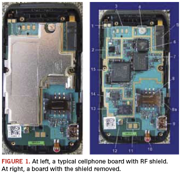
Many different approaches can be taken to address this issue. They include step stencil, multiple printing passes, and an augmented stencil printing process, such as a combination of printing and dispensing/jetting. In the last approach, augmented stencil printing, a single thickness stencil can be used to provide solder paste requirements for the majority of the components, followed by:
- Dispensing more paste for the RF shield, connector, etc. when a thinner stencil is used, or
- Dispensing paste for smaller components when a thicker stencil is used.
The current study takes a step approach to understand the challenges associated with noncontact dispensing, better known as jetting, associated with both large-volume jetting and ultra-fine dot jetting. Results from the Phase I work are presented.
Solder paste for jetting. Successful solder paste jetting depends highly on paste design and dispenser system design. Solder paste is a critical part of any surface mount process, whether stencil printing or dispensing. As the solder paste printing process is nearly 50-years-old, paste manufacturers have had ample time to optimize paste for printing. However, solder paste jetting is a relatively new process that needs a customized formulation to achieve a robust jetting process.
Key solder paste components important for jetting include:
- Solder powder size.
- Metal content.
- Viscosity.
- Thixotropic properties (the property of fluids that are thick [viscous] under normal conditions, but flow [less viscous] under applied stress).
- Flux type.
- Flux activation temperature.
- Reflow environment.
Among the listed parameters, solder powder size, metal content, viscosity and thixotropic properties are considered most critical for paste jetting. Per Ludwig et al, “The desired solder paste properties include fine solder powder, low viscosity, low metal content, high flux activation temperature, and a high thixotropic index.”2 This work investigates both printing and dispensing of commercially available solder paste to characterize dispensing quality.
Experimental
A two-part approach was taken for the current study. Part one focused on a screening design of experiment (DoE) to determine key dispensing characteristics using a low-metal-content printing solder paste. The second part focused on evaluating commercially available jettable paste using results from part one.
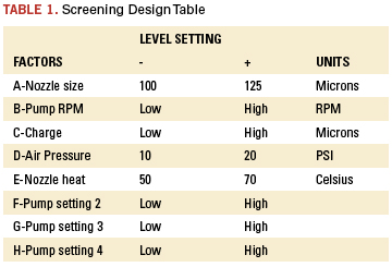
Screening DoE. The screening DoE included eight dispensing system-related factors with one type of solder paste. The paste used was no-clean SAC 305, type IV with 82% metal loading. The dispenser was a Camalot FX-D with SST-500 pump. Table 1 shows design factors and level setting.
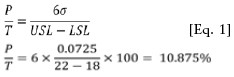
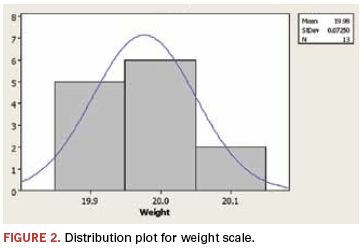
Gage repeatability test. Prior to running the DoE, a gage repeatability test was conducted on the on-board weight scale to ensure the weight scale was capable of detecting the weight variation due to factors manipulation. A total of 20mg of paste was dispensed into the weight cup 13 times to compute P/T ratio (precision-to-tolerance ratio) for the weight scale. The distribution curve for the gage repeatability data is shown in Figure 2, and the P/T ratio is shown below.
The P/T ratio for the weight scale is calculated with a specification limit of +10% of the target of 20mg. The equation and the value for P/T ratio is shown in Eq. 1.
P/T ratio for a target weight of 7.5mg with the same +10% tolerance was calculated to be 30%. Based on the P/T ratio of 10% < P/T < 30%, the weight scale was considered capable.
Methodology. The SST-500 pump was set up according to the manufacturer’s recommended method. The material was purged, and the pump was primed to ensure the system was free of air bubbles and had reached steady-state streaming. After reaching steady state, two types of tests were conducted per run order:
- Predetermined amount of paste was dispensed into the weight cup to determine weight repeatability. Ten replicates per run order were conducted for this phase.
- Following the weight repeatability test, 10 x 10 array of dots and lines were dispensed on a clean board to evaluate the dot size and quality.
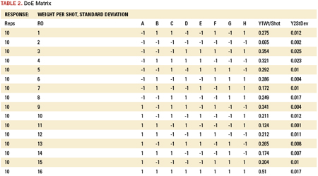
The standard order DoE matrix with the run order is shown in Table 2.
Results and Analysis
The results presented here consider both the mean of 10 replicates and standard deviation as the response variables.
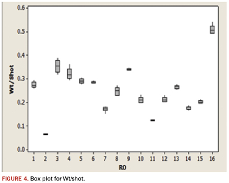
Minitab was the primary statistical analysis tool used for the DoE analysis. The concept of “practical,” “graphical” and “quantitative” analytical approach was taken in analyzing the DoE data. Two major practical analytical methods are highly useful in determining data integrity and high level factor effect: 1. ANOG (Analysis of Goods), and 2. Box plot (and/or run chart). ANOG analysis provides a high-level view of the factor significance and presence of bias in the data, while box plot gives insight to the range and standard deviation of the response variable. Figures 3 and 4 show the ANOG table and box plot for the 16-run DoE. Figure 3 shows spread of response to be between 0.065 to 0.51mg/shot. This indicates that the chosen factors and level settings had a significant effect on the weight/shot response variable. In other words, appropriate factors and level settings were chosen for the DoE. We also see from Figure 3 that several factors (C, D and F) seem to have significant effect on the response. This is indicated by a group of more than 3 “+” or “–” level in the factor column. The box plot, Figure 4, shows the factors and level settings had a significant effect on the response by the random variation of the response. No bias is detected in the response. Based on this analysis, graphical and quantitative analyses were carried out to learn the statistical significance of the factors. 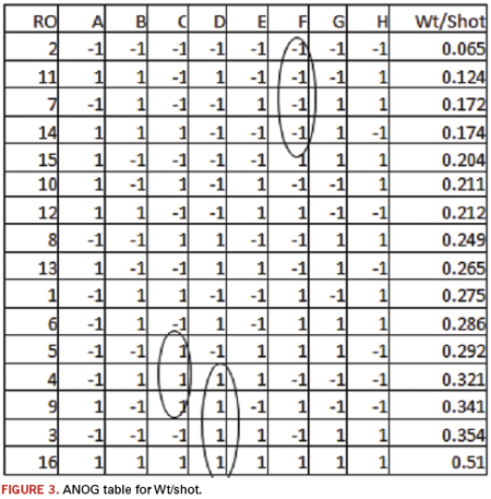
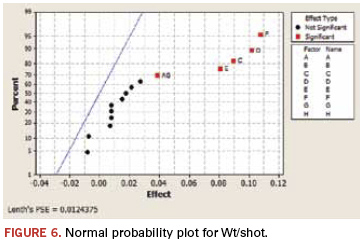
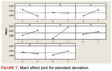
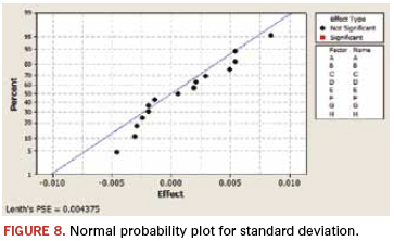
The main effect plot and normal probability plot for both weight/shot and standard deviation are presented in Figures 5 to 8. Four factors (Charge-C, Air pressure-D, Nozzle heat-E and Pump setting 2-F) along with AB interaction statistically, significantly affect the response. When the normal probability plot, Figure 8, for standard deviation is examined, we see none of the factors had significant effect on the weight/shot response. This indicates the experiment was stable, with small standard deviation.

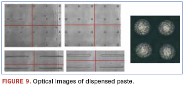
Typical optical images from the experiment are shown in Figure 9. Depending on the factor combination, dot weight ranged from 0.06 to 0.3mg and size ranged from 0.5 to 1mm. Based on the results, several additional DoEs were performed to further understand the effect of critical factors, along with long-term (minimum of one-shift working time) jetting effect.
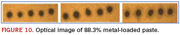
Long-term testing. After two additional DoEs, long-term testing was conducted using a commercially available Type 4 paste with 88% metal loading (printing paste). An automated test was set up to run for 15 hours by dispensing a predetermined pattern onto the weight cup, followed by dot dispensing on a clean board. Figure 10 shows test results. It is clear from the optical images that the dot formation was not as well-formed as with a lower viscosity (low metal loading) paste. Even though the dot quality was less than desirable, it remained consistent throughout the test period. No clogging of the nozzle or pump was observed.
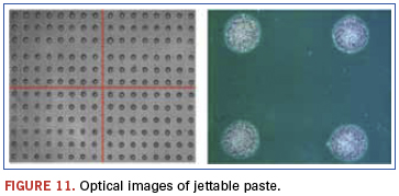
Jettable paste trial. Comparison of jettable paste with standard printing/dispensing paste was conducted using a commercially available paste, design for jetting. Based on the DoE result, an optimum process setup was used for this test. Figure 11 shows the dot quality and size.
Conclusions
A systematic approach to conducting an experiment and analyzing data from solder paste jetting is presented. The results show, depending on the jetting system, only a few factors are critical to the jetting process. These factors will vary from jetting system to system. Based on the experimental data, we make the following conclusions:
- Solder paste type is critical in the success of jetting process. It is feasible to jet high metal loading paste (printing paste type), but the dot/line quality is not acceptable.
- Given the properly designed paste for jetting, it is feasible to deposit 0.5mm dot/line for broadband application.
Additional work is underway to understand the feasibility of jetting solder paste for ultra fine pitch component assembly. Collaboration between material suppliers and equipment vendors is critical to the success of this process development.
Acknowledgments
The author would like to acknowledge Rajiv Iyer and Tom Marjanski, Speedline Technologies, for their invaluable support in providing process knowledge and conducting all the experiments.
References
1. s1.zetaboards.com/Turk/topic/4301811/1/
2. Dr. Richard Ludwig, Dr. Ning-Cheng Lee, Steven Rocco Marongelli, Sergio Porcari, and Sunil Chhabra, “Achieving Ultra-Fine Dot Solder Paste Dispensing,” Proceedings of Advanced Electronic Assembly Conference, October 1988.
Ed.: This article was first published at SMTA International in October 2011 and is reprinted here with permission of the author.
Rita Mohanty, Ph.D., is director, Advanced Development & Application Engineering-Dispenser, at Speedline Technologies (speedlinetech.com); rmohanty@speedlinetech.com.
The phone rang. It was 11:45 p.m. Scott Fillebrown, not nearly awake, answered to learn the caller was reporting the building his EMS company had called home for 19 years might be on fire. Not long after, a second call confirmed the disaster in the making. Driving to the plant, he could see the sky alit from a mile away.
It took more than six hours to extinguish the blaze, which remains the largest ever handled by the Richardson, TX, fire department. The building was decimated; the equipment – including a placement machine so new the company hadn’t even made the first payment – completely wiped out.
Some $2 million worth of equipment was lost that night. But the Automated Circuit Design workers did something unexpected. They collected all the PCs they could, took them home, cleaned them up, and started working again. By the end of the weekend, the servers were brought back online, and the company was again designing and hand soldering boards. Relocated to a site across the street, they quickly upgraded the power and other facilities and were completely up and running with 90 days.
Each June since, on the anniversary of the fire, the company holds a picnic. “You can mope, or understand the blessing and pick up the pieces,” says Fillebrown, the company CEO and co-owner since 1995. Most of the workers from that summer, he adds, are still with the company.
Fast forward to today, and the pluck and determination ACD showed in spades in the aftermath of the fire are showing returns even an optimist like Fillebrown couldn’t have conceived of. 2010 proved a record year in sales for ACD, and through June 2011 was shaping up to be even better – a run rate on pace to top $30 million, good for 25% growth, well ahead of the industry average. The company had further reason to celebrate: An expansion completed earlier this year added 13,500 sq. ft. to the now 52,800 sq. ft. facility, which, coupled with the recent addition of two high-speed lines, gives the plant the capacity to more than double 2010’s sales.
Company and owner have, to great degree, grown up together. Fillebrown, a gregarious Texan in his early 40s, but who looks more youthful, has spent nearly his entire career with ACD. Armed with a degree in business, he joined as a salesman in 1990, having previously worked with the wife of one of the then-owners. After two years, he left for Trend Circuits, but returned as head of sales in 1993, with a pending deal to become an owner. At the time, ACD was primarily a design service bureau that was slowly making the jump into assembly. With no technical background, one of Fillebrown’s first moves was to bring aboard Steve Schwaebler as technical manager. Schwaebler, who previously had managed an operation of some 50 designers, was well-suited for the task. Within a year, he too had bought into the ownership, forming the core of the management and ownership team that exists to this day.
From VARs to Stars
Under Fillebrown and Schwaebler, ACD has made the leap from primarily a frontend printed circuit board design to a full-fledged EMS company. The company for a time even dabbled as a value-added reseller for boundary scan software and other engineering software. Even now, Fillebrown says the firm could easily have taken another path.
“We never intended to be an assembly house,” he says. “But we wanted our own product. Being in the services business didn’t give us the control over our future. So much of services is tied up in a few personnel.”
At one point, ACD was asked to handle prototype bare boards, but struggled finding the right partner. Even then, assembly came about as much by accident as by design. The first hand soldering job the company was ever offered, Fillebrown recalls, came before they even knew how to use the equipment.
Even today, with five full SMT lines and extensive hand soldering and test capabilities, ACD retains its design roots. Design services is a $2 million business and the centerpiece of the company’s turnkey offerings. It’s clearly a point of pride for Fillebrown, who touts the firm’s seven IPC CID designers, with an average of nearly 10 years’ experience at ACD.
“We get a lot of boards that have errors because the electrical engineer laid out the board. We did a study and found 75% of the boards on our floor were ACD designs, but only 10% of the errors were on boards we designed.”
While at most EMS companies designers sit in cubicles or a bullpen, at ACD they have their own offices. There are two reasons for breaking with tradition, says Schwaebler: “One is to allow them to really concentrate on their work. Also, if a customer comes in and wants to work on the design, it gives them the space to do so.” Schwaebler, a former designer who came up in a bullpen setting, also acknowledges the prestige the office gives.
Within the past year, however, ACD began to see customers attracted as much for the board assembly as for the design services. ACD handles four to five new part numbers per day, and has 300 to 400 individual product builds in progress at any given time. A dedicated user of Mentor Graphics’ Valor tools, ACD offers lifetime design for assembly analysis for a specific part number for a one-time charge. The firm also uses Valor tools for stencil design, and runs a paperless factory thanks to CircuitCAM. Several large touchscreen monitors are prominently featured throughout the factory, showing the status of work in progress.
The monitors aren’t the first thing one notices, however. Rather, it’s the ceiling and flooring. The ceilings in most places are low by most EMS company standards. But Fillebrown says that, at 10 ft., they are tall enough to accommodate the largest equipment in the factory, and the company saves immensely on heating and cooling, not to mention the reduced noise.
The floor, meanwhile, is carpeted throughout, which jolts some unwitting customers who do not realize it is completely ESD-proof.
On the floor are five SMT lines, all with DEK printers and Heller 1809 reflow ovens. Three higher mix, lower-speed lines use Mydata MY15e placement machines, one line being a Synergy Dual 15e, while the high-speed lines use four recently purchased Juki FX-3XL and two KE 3020XL pick-and-place machines. Handlers are from Nutek, and a YesTech YTX-3000 x-ray is also present. An Electrovert wave soldering machine is on order.
ACD offers full design to box build capability, including bare board procurement, which is typically sourced through DDi, TTM Technologies or Marcel Electronics Inc. (MEI). While ACD tries to keep inventories lean, Fillebrown has been known to suggest customers buy up to a year’s worth of boards in advance, pointing out the time to market advantage, and adding that the price breaks for the additional volume could conceivably pay for any unused boards up to three times over.
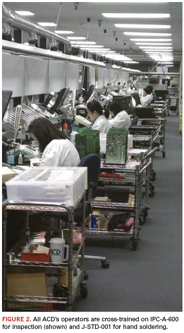
Most of the floor space – 30,000 sq. ft. – is occupied by QA inspectors and prototype PCB soldering using Metcal irons. ACD designs to IPC-2221, inspects to IPC-A-600 and IPC-A-610, and all operators are cross-trained on IPC-A-600 and in hand soldering they are trained to J-STD-001.
Selective soldering and cleaning are performed in a small room off the hand-soldering floor. ACD uses two ACE selective machines, a KISS 102 and KISS 104, with ProMation loaders. Cleaning is performed on a four-batch Aqueous Technologies Trident defluxer, and an older Asymtek conformal coater is available too.
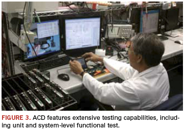
The test area is another point of pride for ACD. There, four machines run constantly, including two Seica S40 Pilots and two Acculogic Flying Scorpion FLS8100 double-sided flying probes, performing boundary scan, functional test and ICT.
A small box-build operation completes the picture.
Fillebrown is bullish on the company’s prospects, though he notes that much of the recent growth has come from market share gains instead of greater demand. Although in-state orders make up 90% of ACD’s revenue, medical has become its second-largest end-market, at about 25%. Not surprisingly, given the proximity to several major semiconductor companies, semi is the firm’s largest market, and ATE is third. Defense and aerospace is fourth, but somewhat cyclical.
A 27-year-old with no technical background buys a PCB business. A design services bureau jumps into electronics assembly, and just as the industry was pulling out of its worst recession and a company literally in cinders makes the decision to rebuild. Three game-changing decisions, all with the best possible outcome.
Automated Circuit Design is on fire again, but this time it’s by design.

Mike Buetow is editor in chief of CIRCUITS ASSEMBLY (circuitsassembly.com); mbuetow@upmediagroup.com.
The annual rankings of the world’s largest PCB fabricators are, once again, dominated by Southeast Asia.
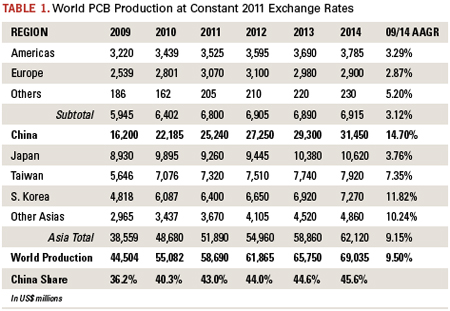
Worldwide printed circuit board output grew 23.8% year-over-year in 2010, fueled by – where else? – China, which grew 37%. Considering the ongoing and near-term expansion taking place in China, the nation’s PCB output will outpace all other regions per Table 1. The 101 largest (by revenue) fabricators produced approximately 80% of the total worldwide output in 2010. As we’ve noted many times, there is a clear trend that the bigger companies grow faster than the smaller ones.
In this annual report, we present a list of world’s top 101 PCB makers in 2010, and discuss their trends by analyzing the data from various angles.
Unlike previous years, we did not separate flexible printed circuit assembly (FPCA) from the totals because it is very difficult to separate the assembly values from the total output of those fabricators. Most large flex circuit fabricators generate a major portion of their revenues from assembly, however.
Also, some major mergers and acquisitions took place during 2010. Regardless of the dates of acquisition, these activities are assumed to have taken place on Jan. 1. Finally, the fiscal years of AT&S and most Japanese fabricators ended on March 31.
Exchange Rates
Exchange rates play a major role in the rankings. Taiwan manufacturers seem to convert their NT dollar-based output to US dollars every month. In this report, the author used “average exchange rates” to convert output in local currencies into US dollars for comparison purposes, as listed in Table 2.
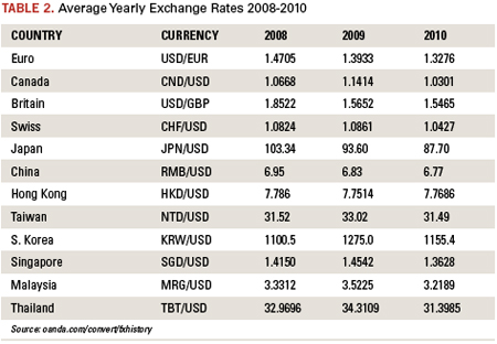
The output reported by some Chinese makers included value-added taxes (VAT), which have been deducted. Moreover, close to 1,500 factories in China are operated by more than 1,100 manufacturers. As the author is not fluent in Chinese, he may have missed some important manufacturers that own multiple factories under different names. Every effort will be made to improve the data through better understanding of Chinese makers. Revenues of some manufacturers such as Foxconn (FAT) are based on calculated guesses, because the company does not break out its revenues. (If you know, please inform the author.)
Finally, keep in mind the rankings are “relative,” not “absolute.” If readers are dissatisfied by the rankings in the tables, please make your own corrections and judgment. Also, the author made maximum efforts to present as accurate a number as possible, but given human fallibility, there may be some errors. Please excuse the author for any errors, for which he takes full responsibility.
Summary of Top 100
In 2010, a total of 101 companies had PCB sales of $100 million or more (Table 3). Total (domestic and overseas) production by Taiwanese PCB makers in 2010 is estimated to have been $17 billion, while No. 2 Japan topped $14 billion. These two countries accounted for 56% of the world production. Table 4 shows why. Their respective investments in China and Southeast Asia in fiscal 2011 will amount to approximately $2.5 billion, which puts these two countries in position to continue to dominate world production.
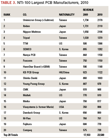
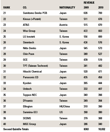
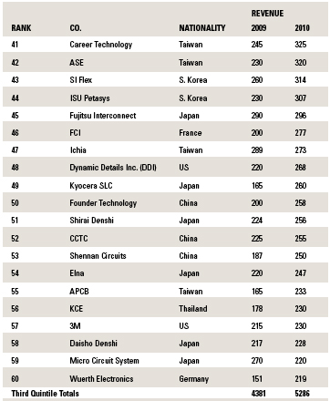
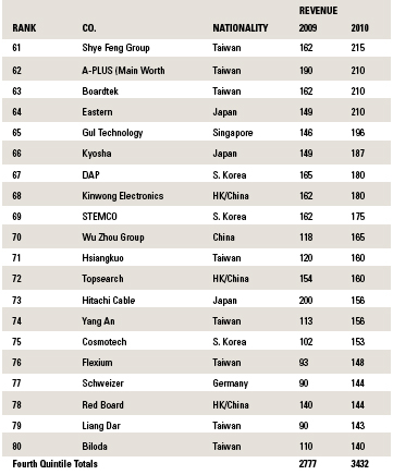
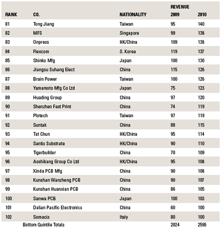
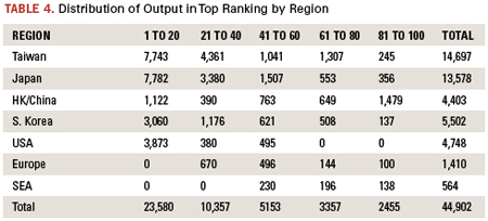
Hong Kong and Chinese fabricators are moving onto the list quickly, as one can see from Table 3 (an aggregate $1,379 million in the bottom quintile) and Table 5 (13 entries).
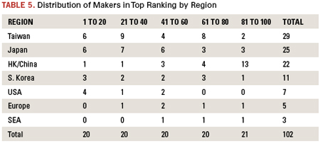
US-based fabricators actually build more boards offshore than they do in the US. To wit, it took about 320 US fabricators to produce $3 billion in 2010 domestically, while just six US-based fabricators (TTM, Viasystems, Multek, M-Flex, Sanmina-SCI and 3M) produced some $3.1 billion overseas. Because of their vigorous investment overseas, offshore production by US-based manufacturers will continue to grow, while domestic production will oscillate around the $3 billion level.
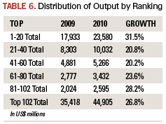
Table 6 underscores the “big get bigger” trend. At the same time, the growth rate of smaller manufacturers ($80 million to $150 million per annum revenue) is greater than their middle-class counterparts. This is driven by the China-based manufacturers, while mid-tier fabricators in “the west” are stagnant in terms of revenue growth. Big fabricators continue to expand because their big customers do not wish to increase the number of suppliers. Small ones have no fear. Middle-class makers are sandwiched between these two classes.
Dr. Hayao Nakahara is president of N.T. Information; nakanti@optonline.net.
Listen: Your SPI might be trying to tell you something.
Does anybody really believe that in 2011 three-fourths of all SMT defects are generated in the print process? Of course not. But we accept this spurious, decade-old, seemingly baseless statistic on stencil printing without question because we know how important a good printing process is to a profitable SMT assembly operation.
So we buy super-expensive inspection machines and reconfigure our assembly lines to accommodate them. We tout their superior GR&R of less than 10%. But when the inspection machine flags a print as bad, we have an operator look at it under the microscope and pass it down the line if it looks good to their “trained eye.”
Seriously? Then why purchase the machine? What’s the point of setting specific inspection parameters on a sophisticated tool, only to overrule them with far coarser and less accurate measurements? I’ve heard a number of reasons for passing flagged prints down the line, but to me they sound more like lame excuses than valid justifications.
When an inspection system fails a test specimen because a measurement does not meet user-defined criteria, I think it is up to the person who set the criteria to investigate why. I’ve spoken with a number of SPI power users, and they all echo similar thoughts on the topic: “When the machine fails prints, it’s trying to tell you that something’s wrong. You have to listen to it and do some engineering to find the root cause.” A few of the gurus shared interesting stories in support of their assertions:
- During the validation testing of a brand new, electroformed stencil, the SPI system flagged half the prints for an odd combination of excessive and insufficient paste volumes. Typical defect modes on these PCBs might be one or the other, but rarely are the modes so mixed. The deposits and apertures looked fine under the microscope, so the engineer measured the stencil thickness in all four corners of the print area. That’s where he found the cause of the variation – a thickness differential of over 0.0025" (that’s 50% of the foil thickness itself!) presumably caused by current density fluctuations during the electroforming process.
- A different assembler found a similar stencil problem when firing up a new product on his line. The print volumes on one QFP kept reading high, but the prints themselves looked great: nice bricks with straight sides and flat tops – no peaks, dog ears, strings, or other visual indicators of excessive paste. A series of measurements revealed that the stencil supplier had mistakenly cut a 0.006" foil instead the 0.005" that had been ordered. Had the engineer simply permitted the visual assessment to override the machine’s measurement without investigation, that stencil would have been placed into production, and would have likely caused lower yields due to suboptimal solder volumes; small features would have gotten less solder than they needed due to decreased area ratios, and larger features would have experienced more bridging due to the excessive volumes and slumping. The resulting yield hit would likely only be a couple percentage points. It could have flown under the radar for a long time, given that this was a new product and there was no baseline for comparison.
- Another series of excessive volume readings – not necessarily rejects, but readings consistently in the 130% range – led engineers at a third assembler to measure the stencils and PCBs. They found the PCB pads were overetched by nearly 0.002", barely meeting the minimum size specification. But the pads met the spec, so the PCBs could not be rejected for quality reasons. The stencil apertures were already cropped for fine-pitch devices, so the size mismatch was about 0.001" – just enough to cause minor gasketing problems and permit excess paste to pump out along the gap. Understanding both the root cause and the degree of risk associated with running higher paste volumes, the engineers decided to open the upper tolerance limit for the remainder of the PCB lot. While I don’t normally advocate opening inspection tolerances to eliminate “false” calls (not truly false calls – just the ones that would be foolishly overridden anyway), in specific cases like this, it makes perfect sense. In fact, that’s why we like our tolerances to be programmable in the first place.
Three different PCB assemblers, three different stories on why we should listen to what our SPI systems are trying to tell us, and in all three cases, a little engineering legwork found the root cause of the problems. Interestingly, in all three cases, the printer and paste were working just fine.
Stencil printing is not just about the printer and the paste; if it were, the process would be a whole lot easier to manage. It’s about the entire system, including PCBs, stencils and squeegees (or print heads), and it’s the systemic interactions that make the process complicated, interesting and fun.
Next time the SPI flags bad prints, don’t pass them down the line with the assumption that the printer is fine. It probably is. While the SPI machine can’t tell you exactly what is wrong in the print system, it can tell you that something is wrong, and it’s up to you to listen to it, identify the root cause, and try to prevent the problem from happening again. After all, that is what process engineers get paid to do, isn’t it?
Chrys Shea is founder of Shea Engineering Services (sheaengineering.com); chrys@sheaengineering.com. She wrote this article on behalf of Christopher Associates (christopherweb.com).

When it comes to heat transfer, bigger is not always better.
True or not true? When you need thermal vias, more is better; bigger is better.
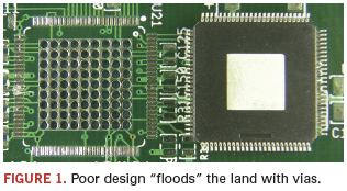
Logically, this would seem to be the case. There are limits though, especially if you want a reliably assembled product. Older parts with heat slugs easily accessible for bolting on heatsinks didn’t have this issue. Just bolt on a piece of metal and maybe blow a fan across it. It’s different with a lot of the new, smaller surface mount packages. Many have a heat slug on the bottom, which requires carefully placed thermal vias to a copper pad on the underside of the board.
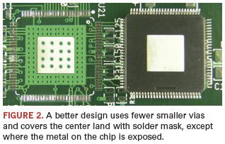
An extreme case of flooding the land with vias can be seen in Figure 1. In terms of assembly, you can hack this together for a prototype, but it’ll never fly in a production environment. It would be much better to use fewer smaller vias and have the center land covered with solder mask, except where the metal on the chip is exposed, as in Figure 2.
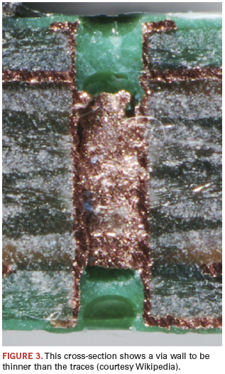
On the subject of vias, I’m sure you have seen charts on the current carrying capacity of traces, but what about vias? That’s a good question. I’ve heard that you first need to know the thickness of the via wall. Then, once you know that, the trace-width equivalent for the via can be calculated by using the formula for the circumference (diameter x ∏). For whatever number that gives you, compare the closest smaller trace width.
Now here’s a question for all you PCB fabrication gurus out there: Since vias are not created in the same way as the trace plating is, can that simple formula be used? While the trace copper is laminated onto a nice smooth PCB surface, the vias are typically created by deposition of copper dust in the via and then electroplating more copper. Then the surface finish is applied to all of the exposed metal. The via walls would generally be rougher than the flat substrate surface. Does that have an impact on the current capacity of a via?
Further, since airflow will be somewhat restricted in a via relative to a surface, should the via’s effective width be compared to an internal trace instead of an exposed surface trace? Should it be a compromise between the two?
Look closely at Figure 3. The via wall looks thinner than the traces. You’ll have to make sure your board fabricator can give an accurate thickness of the via wall.
Ed.: Read Duane’s blog each week at circuitsassembly.com/blog/.
Duane Benson is marketing manager at Screaming Circuits (screamingcircuits.com); dbenson@screamingcircuits.com. His column appears bimonthly.
A well-conceived program can save money and materials.
Developing an EMS (Environmental Management System) can be beneficial to an electronics manufacturing services company. Benefits include monitoring and complying to regulatory requirements, setting and completing environmental objectives and pollution prevention. By setting either an objectives oriented program or a continuous improvement program, an organization can reduce costs and receive potential cost paybacks for activities such as recycling.
An EMS is a management system that creates processes to evaluate and control its environmental impacts and aspects, and comply with local, state and federal regulatory requirements. Many resources are available through state and federal environmental websites to develop an EMS. Upon development, certification can be achieved from the International Standards Organization (ISO).
Monitoring and compliance to regulatory requirements. The environmental regulations landscape continues to be very dynamic with state, local, federal (EPA) and electronics industry-related rules such as RoHS (Restriction of Hazardous Substances) and REACH (Registration, Evaluation, Authorization and Restriction of Chemicals). By setting up a system, a facility can monitor and comply with the constantly changing regulations in the US, Europe and the world.
The initial step is to catalog and make a list of the permits and reports, such as air release permit, water discharge, hazardous waste permits and reports, etc. Link the permit and report to the agency and regulation that governs the requirement. Upon making the list, verify the regulatory requirements. This can be accomplished by reviewing the requirement on the state or federal website (epa.gov) or by attending workshops. The EPA provides training on such matters as TRI (Toxic Release Inventory) compliance. This workshop helps businesses prepare the TRI report, which contains a facility’s evaluation of its materials handling and determination if a release threshold has been surpassed. As an example, for EMS companies, if 100 lb. of lead solder is used and released to the environment by offsite storage (manifested hazardous waste) or through recycling activities, a report must be completed and submitted to the EPA and state. Global environmental regulation updates can be received differently; workshops are available through trade organizations or by electronic update exchanges.
As a part of the compliance system, a review can be conducted of what was learned or changed and how it impacts the manufacturing facility. This review or audit can be completed after each workshop or on a yearly basis.
Environmental objectives and pollution prevention. Reducing facility impacts to the environment can be achieved by deploying an environmental objectives program. Examples of environmental impacts include release to air, water and soil and are usually regulated by the facility’s environmental permits and reports. This program can be incorporated into existing quality improvement or Lean manufacturing processes. Consider pollution prevention, waste minimization and green design when incorporating new processes, products or materials. A major component of an effective objectives program is recycling.
Recycling opportunities. Many opportunities exist to recycle within an EMS company. The foundation of recycling begins with glass, plastic bottles, paper products and cardboard. The recycling of printed circuit assemblies, subassemblies, mechanical hardware, components and solder may result in a payback for the metals extracted and refined. Diligence is required before deeming the material recyclable, given hazardous substances and state and federal regulations. Recyclers will shred the item and extract the metals such as tin, copper, silver, etc., which, given current metal prices, may provide a cost payback. Solder dross (lead and lead-free) is one example of material that can be recycled, given its characteristics and metal content. Other opportunities include computer equipment, printers, packaging materials and scrap metal, such as piping, tooling and fixtures.
Reuse of packaging and handling materials. In many cases, the best recycling approach is to reuse the item. This can be best accomplished with packaging and handling materials. Cases may surface in which the packaging material is not recyclable; this may result in a redesign to recyclable material or reusable packaging. Upfront design will be needed for this determination, ideally before product introduction.
Figure 1 can be used to calculate energy savings for the recycling activities at the EMS facility. The metric is calculated on the assumption that recycling saves energy verses the total manufacturing process of creating new material. In the example below, the kilowatt per hour (KWH) savings was based on one ton of paper, cardboard, glass and plastic bottles recycled.
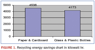
The combined total energy saved is equal to approximately the average household energy use for one full year. Calculators are available through state and federal (EPA) environmental departments and websites.
Other opportunities for projects include energy reduction through lighting and motor improvements and chemical, waste and material reductions. In most cases, energy objectives can result in a cost reduction, usually by modifying lighting times and upgrading lighting fixtures and motors to energy-efficient equivalents. It is important to understand the simple payback of the project; on occasion, rebates are available that can be factored into the calculation.
Potential cost and environmental payback. In addition to the benefits of completing environmental objectives and pollution prevention, cost reductions and paybacks can be potentially received. Electronics recycling, given the current market of metal pricing, provides a cost payback for scrap metal, subassemblies and wave solder dross. Figure 2 details an approximate cost payback per 1000 lb. of wave solder dross, aluminum cans and metal.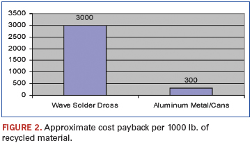
The biggest payback would be from the wave solder dross, which will be refined by the recycling supplier and associated metals (tin, copper, silver, etc.) extracted. Depending on market conditions, cardboard and paper recycling may also provide a payback. Some recycling activities will not result in a cost payback; the result will be the environmental benefit of the material not being discarded in a landfill.
Conclusion
The actions above can all benefit the environment. Moreover, EPA and state recognition and awards are available to successful companies. Employee involvement is important to any recycling program, given their knowledge of the process and products. Employees also have impacts on energy reduction, waste disposal and handling. A material or item that has been historically thrown away may be recycled or reused; employee involvement will bring attention to these new opportunities.
By setting up an environmental management system, a facility can monitor and comply with regulatory requirements and set up a program for environmental objectives and projects. In some cases, the results of the environmental project can provide a cost reduction or cost payback. By training and involving employees, many recycling ideas will surface to the benefit of the environment and manufacturing facility.
Scott Mazur is a manufacturing staff engineer and environmental management representative for Benchmark Electronics (bench.com); scott.mazur@bench.com.
References
1. Scott Mazur, “Environmental Recycling for the EMS” – SMT, October 2010.
2. Scott Mazur, “Developing an Environmental Management System for the Electronics Manufacturer,” IMAPS New England Symposium, May 2011.
