

A benchmark study of cost as a function of various yield rates and line capacity.
Calculating rework and scrap cost is relatively straightforward, provided the production line’s first pass yield (FPY) is known. The cost of low yield is simply the difference in rework and scrap between the manufacturer’s production line and that of a benchmark line. The benchmark figure for stencil printing is around 10 dpm (defects per million), and that for a pick-and-place machine is now 5 dpm. Allowing for defects from PCB manufacture and reflow soldering, that gives a whole-line benchmark of below 30 dpm.
Compared with a typical whole-line defect level in the industry as a whole of between 50 and 100 dpm (just for standard components – the dpm for miniature components such as 01005 types can be 200 or more), that might seem wildly optimistic. The Czech plant of automotive equipment manufacturer Alps Electric steadily attains a level of around 25 dpm, though, for an average of 1 to 2 billion components per year.
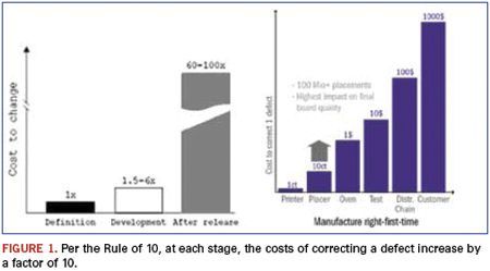
The costs of quality can easily outweigh labor costs. So, even in countries with low wage costs, the savings can be huge. For a typical board with, say, 1,000 components, a whole line quality of 25 dpm gives a benchmark FPY of 97.5%. A line producing 100 boards/hr. (100,000 components/hr.) will need one rework station. Assuming a typical three-shift operation, three operators will be needed for rework. In practice, inline repair will find 90% of all defects. The remaining 10% will be detected at a later stage, increasing repair costs by a factor of 101 (the Rule of 10) at each stage (Figure 1).
Annual labor costs average $2,800 to $4,200 in Southeast Asia, $7,000 in Mexico and Eastern Europe, and $40,000 to $65,000 elsewhere. That gives total repair costs per 25 dpm line of $35,000 to $410,000 per year. By contrast, a typical 100 dpm production line would have a yield of 90% and would need two rework stations with repair costs of up to $625,000. And, because defects often come in batches, the lower the yield, the more random the effects and less predictable the output. Rework lines can be underworked one day and stacked to overflowing the next.
The principle of Six-Sigma quality is to keep processes not just within specification limits – what a customer asks for – but within control limits that are repeatedly well inside specification limits (high process capability). That means processes can drift, but still produce good output while faults are being corrected. This is basic quality improvement theory, and is also critical to successful (and profitable) electronics manufacture.
Reaching benchmark performance means optimizing each of the three major surface-mount processes: stencil printing, pick-and-place, and reflow soldering. Solder paste printing needs to select the correct stencils, apertures and printing parameters for components being used, with regular monitoring of stencil cleaning and paste replenishment. Each process step of the pick-and-place machine needs to be monitored and working well within specifications. Reflow soldering needs the correct reflow temperature profile with accurate process control. There are several key signs of manufacturing processes going out of control, and they tend to fall into distinct classes and with distinct causes. Identifying those signs helps trace faults quickly to bring the process back into control.
In practice, the major influence on production line quality is the pick-and-place machine. And the major quality figure for a pick-and-place machine is the defects per million level, since that reveals the expected yield.
Calculating Yield
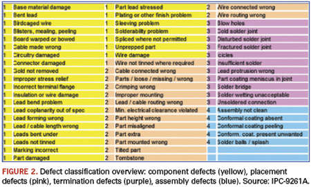
Three related IPC documents (IPC-A-610D, IPC-9261A and IPC-7912A) describe how to calculate yields for a particular board on a particular production line. The standards distinguish the types of SMT defects (Figure 2), and count the number of possible opportunities for defects on each board, which depends primarily on the board’s complexity.
Each component can itself be defective, can be incorrectly placed, can have either of its terminations incorrectly soldered, or (sometimes) have an incorrect process step like a missing conformal coating. Each of those is counted as a single defect opportunity. So a chip component can be cracked, or incorrectly placed, or have one of its two terminations incorrectly soldered, which equals four defect opportunities. Similarly, a QFP52 has a defect opportunity of 54. Adding all the individual component defect opportunities gives a figure for the whole board, and this is normally dominated by the termination count.
The next step is to predict the actual number of defects that a given production line will produce for a board of a particular complexity. That needs a historic value for the actual DPMO (defects per million opportunities) for the line, which any manufacturer serious about improving production quality will track. The DPMO for a board is simply 106 times the total number of actual defects over the total number of defect opportunities. More than anything else, the FPY determines the overall cost of placement. High FPY means low scrap and rework costs, and high return on investment.
The yield is then given by
where Oc, Op, Ot and Oa (Ocomponent, Oplacement, Oterminations, Oassembly) are the defect opportunities. On a board with 1,000 defect opportunities, a single defective placement on 1000 boards would mean a DPMO of 1 and a yield of (0.999999)1000, so 0.999 or 99.9%. A typical board will actually have many more defect opportunities: Table 1 shows a typical board with around 1,000 components having nearly 6,500 defect opportunities.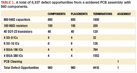
Yield can usefully be calculated over the year. Given 6,000 productive hours in a year and a line cycle time of 40 seconds, that means nearly 3.5 billion defect opportunities a year (540,000*6,337 = 3,421,980,000). With 15,000 defects a year, the DPMO is just over 4 (106*15,000/3,421,980,000= 4.38). That gives a yield of Y = 97.26 % over the year.
Figure 3 shows how yield depends on the number of defect opportunities for various DPMO figures. Every colored line indicates a certain DPMO level. Depending on the quality of the process, the DPMO figure shows whether defect opportunities are converted into actual defects. With a low DPMO, the yield drops slowly and almost linearly with the number of defect opportunities. So, yield remains good for even complex boards. The higher the DPMO, the more steeply the yield drops to zero.
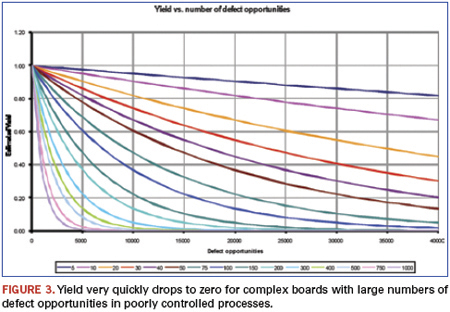
A manufacturer will actually have a window of defect opportunities. Automotive boards, for example, have from around 100 components (entry level) up to 600 components (top of range). Around 96% are resistors and capacitors (defect opportunity of four each), and up to 4% are ICs. ICs mainly include QFP and SO types, with a few BGAs of up to 300 I/Os, giving a total average defect opportunity of, say, five. That gives a total of between 2,000 and 12,000 defect opportunities per board (four-fold board).
Different applications have different defect opportunity windows. Automotive boards tend to have low component counts (but the cost of a defect in an automotive board can be very expensive). For mobile phones and (particularly) communications and server boards, the window shifts to the right. The window for mobile/smartphones is typically between 6,000 and 20,000, and that for complex communications and server boards from 25,000 to 60,000. For all products, the yield drops most for the larger, more expensive top-of-line products. The cost of rework correspondingly increases.
Calculating Rework
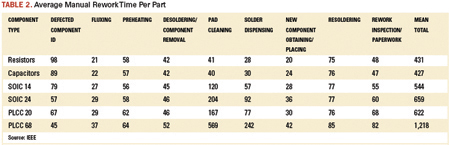
The first-pass yield gives the percentage of boards with good quality, so (1-FPY) gives the percentage of boards needing repair (rework). The average repair time per SMT defect (Table 2)1 gives the related time for rework. For boards with an average of 90% resistors and capacitors, the weighted average per defect is 540 sec., or 9 min.
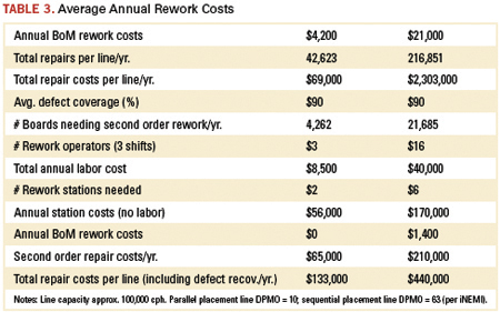
The major determining factor for yield, and therefore, rework costs, is the placement technique. Sequential placement dominates the industry, with machines usually having one or two heads working at very high speeds. Parallel placement machines instead have multiple placement heads (up to 20), so the individual heads have much more time to settle before placing the component. So, for the same overall placement rate, parallel placement machines have a much steadier and more controlled placement action. Even in India and China, the difference in rework for a parallel over a sequential placement machine per line can exceed $300,000 (Table 3).
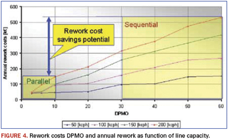
Actual savings depend on line capacity, and are almost double for a line placing 200,000 cph vs. one placing 100,000 cph (Figure 4). The difference between parallel (even at 10 dpm) and sequential placement (at 60 dpm) producing 10 million phones per year in China with 250 SMDs per phone would be around $1.3 million per year. And factories can have 50 or 100 lines.
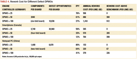
Rework costs are thus a factor of 3.5 lower for benchmark pick-and-place machine lines, and that is just in the low-wage countries. In Germany they can rise to $1.2 million per line per year for automotive engine controllers (typically 340 components per circuit, six circuits per board, around 10,000 defect opportunities per board and a line capacity of 130,000 cph). That permits manufacturers to keep their production lines in the West, saving on distribution and logistics costs, while retaining all the advantages of short supply lines.
Even in the best-controlled processes, defects tend to come in groups. In well-controlled processes, though, the reasons for the defects can be quickly found and corrected. Actually finding the defects, however, is becoming more difficult.
No quality inspection technology provides 100% reliable coverage. Research by Nokia and the University of Oulu in Finland shows most technologies provide around 90% coverage, leaving 10% of all defects undetected. Finding detects therefore requires a combination of AXI, ICT and AOI technologies. Even then, though, some defects will slip through. This demonstrates a basic quality principle: You can’t inspect quality into device, but instead have to improve the process.
State-of-the-art screen printers offer process quality below 10 defects per million components. The industry DPMO for stencil printers is above 25 dpm. For pick-and-place machines, it is around 25 dpm, with the worst giving 50 or more. Compared with a whole-line benchmark figure of 25 dpm, typical and poor figures would be 50 and 100, respectively. Per Table 4, a complex smartphone produced on a whole-line DPMO of 25 would give a 59% yield. For a DPMO of 50, the yield drops below 40%, and for 100, it is an impossibly low 12%.
These are the visible costs. As the Rule of 10 suggests, detecting a defect at final test costs 10 times more than detecting it immediately after placement, 10 times more than that at the retailer, and 10 times more than that in the shop.
And recent quality problems in well-known car brands illustrate another basic rule of quality improvement: Faults that escape to the customer are the most expensive of all – in damage to reputation.
References
1. IEEE Transactions on Electronics Packaging Manufacturing, vol. 26, no. 2, April 2003.
2. Dr. David M. Anderson, “Design for Manufacturability and Concurrent Engineering,” CIM Press 2008, ISBN 1-878072-23-4.
Sjef van Gastel is manager of advanced development, Assembléon (assembleon.com); sjef.van.gastel@assembleon.com.
The universal truth is, don’t overdo it!
Want the most bang for your buck on PCB purchases? Four industry veterans with backgrounds in PCB materials, chemistry, fabrication and assembly provided their expert advice, often echoing each other’s recommendations. If you want to maximize PCB quality, price, performance, delivery or overall value, try following some of these insiders’ tips:
Get a first-article inspection. Testing a preproduction sample is essential to determining if the fabricator can meet your quality requirements. As Mike Carano, global manager of strategic business development at OMG Chemicals, explains, “I see many fabricators fail badly when making a new part number. Not because the company is not of high quality, but because they actually lack experience with the design and material sets in question.” He suggests asking the fabricator to build test coupons to measure registration, via formation and PTH reliability.
Get pricing up front. The bottom line is exactly that – the bottom line. A myriad of factors go into PCB pricing, so it’s best to know if the fabricator can meet cost goals before you invest time and money checking quality or visiting facilities. For help determining fair pricing, download a PCB cost/sq. in. calculator (pcgandg.com/Pricing__The_Smoking_Gun.html).
If pricing seems reasonable, Erik Bergum, industry veteran and former chair of the IPC Base Materials Committee, advises giving it a closer look. “PCB purchasers should know the setup and lot charges for tooling and test, and understand which charges recur and which ones don’t,” he says. “Before issuing the initial PO, capture the cost and delivery timing for the first set of boards and for the subsequent sets.”
Always check the fab drawing. This is the place where materials, finishes, plating and any special directions are communicated. Pay attention to these callouts. Chrys Shea, PCB assembly expert and president of Shea Engineering Services, advises, “If you have qualified a particular material for storage, processing or reliability reasons, make sure the words “or equivalent” do not appear in its callout. Those two words invite unwanted substitutions that will likely disappoint.”
In some cases, especially when expensive metals are involved, more specificity is recommended. If ordering ENIG final finish, Carano suggests explicitly stating the following requirements: 150-220 microinches of nickel, with 150 as the stated minimum, and 1 to 2 microinches of gold. He also suggests calling out a minimum plating thickness of electroplated copper in barrels of 0.0008" or 20 µm, explaining that “anything less should be cause for rejection. The 0.0008" minimum is derived from hundreds of thousands of hours of reliability and field data. This is how we build reliability into the hole.”
Check UL certifications online. Go to ul.com and look in the lower right corner of the header for a button labeled “Certifications.” Clicking it will bring up the online certifications library, where you can look up the fabricator’s UL certifications. If you can’t find a fabricator, or if they are not certified to manufacture the narrowest conductor width on your board, contact them to resolve the discrepancy. If your PCB distributor holds the certification instead of the fabricator, you should understand that as well. You have the right to know who manufactures your circuit boards and the UL stamp source.
Ask for dummy boards. Also known as X-outs, electrical test failures, profile boards or solder samples, bare PCBs with quality problems that cannot be assembled and sold are great for profiling, pick-and-place tuning, process verification, or other engineering experiments on the assembly floor. How to get them? Just ask. As Tech Circuits senior applications and quality engineer Lee Starr explains, “Like all manufacturing processes, PCB fabrication is subject to yields that are typically based on design complexity. When a fabricator begins a lot of PCBs, they start more boards than the order calls for, based on their estimates of expected yield. While good boards are shipped to the customer, bad ones are reclaimed with little value to the fabricator. NPI engineers routinely ask for them, but production shops usually don’t.”
Shea adds, “During the production life of a circuit assembly, it can be built on different assembly lines, in different factories, or even in different parts of the world. Due to considerable variation among reflow oven performance, an assembly should get reprofiled each time it is run on a new line, but this doesn’t always happen – often due to cost constraints. The availability of profile boards at zero cost to the assembler vastly increases the odds of the assembly getting profiled and reflowed properly, minimizing solder defects and improving overall reliability.”
Don’t overspec it. If a little is good, a lot is better, right? Wrong. Adding an unnecessary “safety margin” to material properties may create unexpected issues. Bergum warns, “If you overspecify critical properties such as glass transition temperature (Tg), degradation temperature (Td) or Z-axis expansion, you may find that the specialized materials often have sensitivities to processing, handling or storage that may negatively impact yield or cost. Your best bet is to specify materials that meet your performance criteria, and address any questions or uncertainties directly with the fabricator or laminate supplier.”
Don’t overdesign the board. While designers may be very good at electrical design and layout, they are not necessarily good at understanding the interactions of materials and machines, and plating limitations. Carano advises a DfM review by the fabricator to identify opportunities to reduce costs or improve yields. Starr seconds that opinion, offering, “If using a new technology such as 0.3mm BGAs, get advice ahead of time on layer interconnect strategies, target and capture pad sizes, fine lines and spacing. This will ensure producibility at multiple suppliers and help keep the design cost-competitive.”
Don’t “design for panelization.” Designers often make assumptions about vendor panel size, and in an effort to manage unit cost, set the dimensions of individual PCBs to maximize the number of pieces that can be fit onto each panel. While their intentions are good, they may be disappointed to find their efforts are in vain.
Starr explains: “If multiple lamination cycles are required, the usable space on the panel becomes limited. The stretch and shrink of each heat/pressure cycle creates dimensional instability that can cause misregistration near the edges of the panel. As the number of laminations increases, the size of the ‘sweet spot’ in the middle of the panel decreases. The fabricators’ CAD department accounts for this when they perform the panel layout, using as much of the sweet spot as they can for each design, but avoiding areas around the periphery that might cause quality problems. Also, panel sizes vary in offshore fabricators, so the shop’s location becomes a factor. Designers get frustrated when they find out they compromised their desired PCB size or certain design characteristics to accommodate a panelization layout, and their noble efforts were all for naught. Their best bet is to design the single PCB they want, and refer panelization and cost-reduction opportunities to the fabricator’s CAD team for expert guidance.”
Don’t expect high quality just because the shop has ISO 9001 certification. ISO certification means the business’ processes are documented. It doesn’t guarantee high-quality output from the operation. All it guarantees is that almost everything done in the operation is written down somewhere, and an auditor spot checked multiple areas to see how well the records reasonably matched the actual processes.
Certification indicates that a shop has a quality system in place, and everyone agrees that’s a good thing, but they also agree that quality output depends on a great deal more than just the presence of a system. It should be considered a minimum requirement of any new supplier, but certainly not the only one.
Don’t try to cut costs by cutting the PCB broker out of the loop. Broker/distributors combine the purchasing power of multiple clients, so they often have more leverage with fabricators than singular buyers, especially with offshore fab shops. And while it’s true that brokers turn a profit as they turn your PCBs, odds are you will pay a lower unit price than if you go it alone. Plus, brokers’ leverage extends beyond pricing: You can often receive better quality, delivery and response to last-minute changes by sourcing through their established supply network.
Regardless of where you sit in the supply chain, these tips are fairly universal. And although each is targeted to a specific goal of improving cost, quality or reliability, in the end they all help meet the overriding goal of any business: profitability.
Au: Many thanks to Mike, Lee, Erik and Chrys for sharing their expertise and insights.
Marissa Oskarsen, aka The Printed Circuit Girl, owns E-TEC Sales (pcgandg.com); marissa@pcgandg.com.
A new solution involves high-energy conduction heating and custom tips.
Radio frequency (RF) shields are used to separate areas of a printed circuit board (PCB) assembly from each other and to reduce noise and prevent radio signals from escaping from the product and affecting operation of other devices. Antenna products, cellphones and wireless electronics require RF shielding either mounted to the PCB or incorporated into the packaging that surrounds the electronics.
RF shield rework is difficult due to continually shrinking package sizes, reduction of pitch and reduced clear space available around components. This increased density and complexity drives new techniques for removing and replacing RF shields.
Shields are attached to PCBs via two common methods. Both methods attempt to completely cage a specific area by soldering to surface connections to ground planes internal to the PCB. In one method, a metallic “fence” is attached around the perimeter of the area to be shielded (Figure 1). A spring-loaded metallic “lid” is then snapped over the fence to enclose the area. The mechanical contact of the lid and fence creates the RF shield.
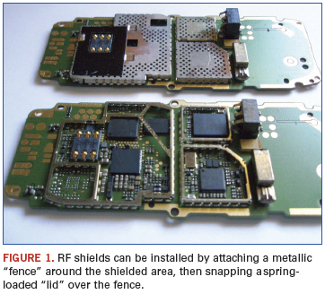
The fence can be added anywhere during the process before solder reflow. Typically, the fence is manually placed by machine using an odd form assembly system. The lid is manually placed after reflow or by a second automated system, and can be readily removed if components inside require replacement.
The second method is a one-step process that adds the shields during fine-pitch placement. By using one-piece shields presented in tape-and-reel or component trays, RF shield attachment requires no changes in the assembly process. The shields are placed and then soldered directly on the board using a standard reflow process. No additional operators or inline equipment are required. A complete metallic bond surrounding the entire area provides the most reliable RF shield and prevents the end-user from tampering with the device. However, if defective components are found during in-circuit or functional test, or if a device upgrade is called for, the shield must be de-soldered.
Three particular challenges need to be addressed:
- Removing the typically odd-shaped shields from the PCB.
- Restoring the proper volume of solder for new shield attachments. (Depending on the condition after removal, residual solder might need to be cleaned and sometimes can remain, with additional solder paste dispensed to add volume for new shield attachments.)
- Producing repeatable results without special operator skills.
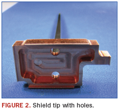
To remove the shield, the nozzle design must conform to the shield’s external shape. There are targeted points at which the shield is soldered to the PCB, and the nozzle needs to be designed so that heat is directed to these areas. This ensures the shield is consistently removed from the PCB without damage to either the board or shield. Attempting to remove the shield before the solder reaches its melting point will inevitably cause damage to the pads on the PCB and render the entire board useless.
Convection is a very common heat source for rework and repair purposes, but for the removal of RF shields, it is not an ideal solution. Creating a temperature adequate to remove these relatively high-mass metal parts without damaging surrounding components and the board itself presents a significant challenge.
Fixed temperature conduction heat. An appealing alternative demonstrating distinct advantages is high-energy conduction heating applied through custom-tooled thermal tips that match the shape of the shields.
When the novel heating element is energized by its high-frequency alternating current (AC) power source, the current automatically begins to flow through the conductive copper core of the heater. However, as the AC current continues to flow, a physical phenomenon known as the skin effect occurs1, and the current flow is directed to the skin of the heater assembly, driving the majority of the current through the high-resistance magnetic layer and causing rapid heating.
As the outer layer reaches a specific temperature (controlled by its heater alloy formula), it loses its magnetic properties. This “Curie point” temperature is when the skin effect begins to decrease, again permitting the current back into the conductive core of the heater and repeating the cycle.
Faster and safer removal. Successful shield removal applications have been demonstrated to reduce the heating time from as many as five minutes using conventional methods to under 45 sec., while keeping the components beneath the shield lid to <200°C. This is a critical concern with glued parts because adhesive expansion in the z axis can be extreme enough to tear the pads.
In Figure 3, the red plotted line shows solder on the shield melting above 217°C. The green and blue lines represent the parts under the shield. In the profile (Figure 3), the first time bar (1.19) shows the preheated time. The tip touches the shields when the PCB is at 84°C.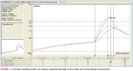
The peak is at 1.42 seconds, which means the contact time – the period the tip was on the shield – was 23 sec. (1.42 – 1.19).
Fixed temperature-variable energy direct conductive heating process provides fast, safe shield lid removal without the problems of adjacent reflow. The process shows potential for providing fast, efficient direct removal of BGA components by delivering heat directly though the component body perimeter and removing the unwanted device without surrounding reflow and risk of damage to the board or nearby components.
References
William Hayt, Engineering Electromagnetics, 4th edition, McGraw-Hill, 1981.
Paul Wood is advanced applications manager at OK International (okinternational.com); pwood@okinternational.com.
Chemical or laser etching coupled with electrical test is a formidable combination.
Decapsulation is a process that has been around for some time and has many different applications. Whether for analysis or verification purposes, the goal is the same: expose the die to perform the task at hand. A few different methods are available to achieve this. Some of the most common are manual etching, fully automated etching, plasma etching and the newest (and more advanced) laser etching.
My exposure to decapsulation has involved all the methods above; however, manual etching has become my primary choice for exposing the die. While more art form than skill, decapsulation has the advantage of leaving the device in question functional, unlike destructive methods such as microsectioning, which literally saws the component apart.
Many factors affect and ultimately determine success. A key aspect to using chemical etching decapsulation revolves strictly around temperature. Too much heat and the acid will react aggressively, destroying the part. Too little heat and the acid-to-mold compound reaction will be slow and messy.
Next is acid deposition. Knowing exactly how much acid to use makes the process controllable, predictable, and makes it much faster, too. Duration will always impact functionality of a device once the die has been exposed. A final key element is device placement. Where and how the part is positioned ultimately sets the stage for a good or bad decap.
While skill is important, exposing the die successfully does require certain items. My primary weapons of choice when performing decapsulation are a hot plate, fuming nitric and/or fuming sulfuric acid. Both acids are equally aggressive, but not all package mold compounds are the same; therefore, knowing how to choose the right acid will ultimately determine success. So how do you know which one to choose? There is no single answer to that question, except trial by error. The acid could either be nitric or sulfuric, and the choice varies depending on the overall appearance of the mold compound surface. Some units require a mechanical approach to expose the die, while others will use slightly different acids. Whichever the case, visual interpretation ultimately regulates the outcome.
Acetone and alcohol are used to help rinse the chemical reaction between mold compound and acid. Whichever of the two acids is selected sets the stage for choosing the correct solvent. It’s a carefully scripted balancing act between acid application, a rinse, and hand-eye coordination that makes manual etching somewhat difficult, but also amazingly unique. The entire process involves 100% control, and the yield, if done correctly, is easily repeatable. Time is solely based on experience, and can take only minutes to complete.
Machine etching has become the more acceptable form of decapsulation, but adds more work to the process, in my opinion. Because it is an automated process, many movable parts are involved. At some point these components will break, require adjustment or need maintenance, none of which is a cheap repair. Also, the machines have no means for neutralizing any of the acids. Acid is heated, ejected from an etch head and onto the specimen. “Cold” acid is then used to rinse the device, and all waste is deposited into one bottle. The contents within the bottles are 100% acid mixed with mold compound residue, and both acid wastes must be kept separate, never combined. Because acetone and alcohol are excellent neutralizing solvents, only one container is needed to capture either nitric or sulfuric waste during manual etching. This is a major benefit in manual decapsulation, where less is always best.
Customers often request units remain functional after decap. At times this presents a challenge, because most devices submitted are considered “golden,” the one and only device available. Functionality becomes more a requirement than an option, and manual etching removes much of the guesswork on how to deliver a functioning unit.
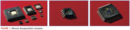
Machine etching is a very convenient way of exposing the die and can produce very promising results. What it cannot do, however, is accommodate sudden changes during the decap procedure to help ensure things don’t go terribly wrong. Control is limited and the entire process depends on a preselected time. Manual etching permits easy adjustments and control during the procedure, and the decision on “how long” is easily changed. Manual decapsulation offers the ability to completely control the etch process (Figure 1).
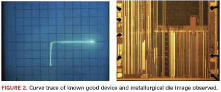
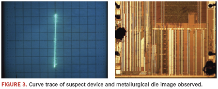
While manual decapsulation is one technique of providing a more conclusive result of product authenticity, electrically testing a device can also help close the gap on pinpointing counterfeit chips. ET aids in identifying faults and inconsistencies on components. A very common method used today is curve trace analysis, which primarily focuses on discovering any parametric damage/differences to the pins of any device of any technology. Combined with decapsulation, electrical damage to the pins on the device can be identified through visual inspection using a metallurgical microscope, which could reveal damage from ESD, EOS, mechanical opens and shorts (Figures 2 and 3).
A recent request from a new customer, Mettler Toledo, revealed the real benefit of having electrical testing capabilities. The devices needed were virtually impossible to locate. When we did find them, they were from different vendors, a situation that increases the chances for counterfeits to enter in the supply chain. We electrically tested the units, with respect to each part’s diode signal curve characteristics. The reasoning was, if all curves observed were all exactly the same, then chances are they were indeed authentic. If they were different, then obviously there was a problem. Normally decapsulation would follow electrical testing, but due to the scarceness of these units, it was not an option. In the end, some 70-plus units were electrically tested, one pin at a time, while applying a small amount of voltage. A diode signal for all the pins tested was observed, and it was their consistency that determined them as good units. Not only did it prove our capabilities as a vendor, but it emphasized the need for electrical testing.
Don Davis is decapsulation specialist at SolTec Electronics (soltecelectronics.com); ddavis@soltecelectronics.com.
Ed.: For more on decapsulation, click here.

FEATURES
BEST Site Visit
BEST: On the Go
From a motor home to a 25,000 sq. ft. factory outside Chicago, BEST not only offers a wide variety of rework/repair services, it is navigating a new path for the EMS of the future.
by Mike Buetow
Bare Die Coatings
Protecting COB Devices with Glob Top Encapsulants
Bare die and their connecting wires have no protective plastic package, and can easily become corroded by moisture or chemicals. Encapsulating the die and wires in a protective shell is critical to ensuring long-term assembly reliability.
by Venkat Nandivada
PCB Repair
Board Repair Made Easy
The small size and spaces make fixing a substrate or interposer a painstaking undertaking. A new novel board repair kit just might be the solution.
by Terence Q. Collier
Rework
Top 10 PCB Rework Mistakes
Why touch-up should be used sparingly, if at all, and other helpful hints.
by Bob Doetzer
FIRST PERSON
-
Caveat Lector
Brokering a new model.
Mike Buetow -
Talking Heads
Asteelflash's Gilles Benhamou.
Mike Buetow
MONEY MATTERS
-
ROI
The design-manufacturing gap.
Peter Bigelow -
Focus on Business
Social media for the EMS.
Susan Mucha
TECH TALK
-
Tech Tips
TSOP bridging.
Robert Dervaes -
Technical Abstracts
In Case You Missed It.
A novel approach to predicting – and improving – device failure rates.
In the long run, we are all dead. – John Maynard Keynes
Vision without action is a daydream. Action without vision is a nightmare. – Japanese saying
Qualification testing (QT) is the major means used to make viable and promising devices into reliable and marketable products. It is well known that devices and systems pass existing QT only to fail in the field. Is this a problem? Are existing QT specifications adequate? Do industries need new approaches to qualify devices into products, and if so, could the existing QT specifications, procedures and practices be improved to the extent that, if the device or system passed QT, there is a quantifiable way to ensure the product will satisfactorily perform in the field?
At the same time, the perception exists that some products “never fail.” The very existence of such a perception could be attributed to the superfluous and unnecessary robustness of a particular product for its given application. Could it be proven that this might be indeed the case, and if so, could it be because the product is too costly for the application so intended, and therefore, the manufacturer spent too much to produce it and the customer too much to purchase it?
To answer the above questions, one has to find a consistent way to quantify the level of product robustness in the field. Then it would become possible to determine if a substantiated and well-understood reduction in reliability level could be translated into a considerable reduction in product cost. In the authors’ opinion, there is certainly an incentive for trying to quantify and optimize the reliability level and, based on such an optimization, to establish the best compromise between reliability, cost-effectiveness and time-to-market for a particular product of interest, and to develop the most adequate QT methodologies, procedures and specifications. Clearly, these might and should be different for different products, different operation conditions and different consequences of failure.
How could this be done? One effective way to improve the existing QT and specifications is to
- Conduct, on a much wider scale than today, appropriate failure oriented accelerated testing (FOAT) at both the design (DFOAT) and the manufacturing (MFOAT) stages, and, since DFOAT cannot do without predictive modeling (PM),
- Carry out, on a much wider scale than today, PM to understand the physics of failure underlying failure modes and mechanisms that are either well established or had manifested themselves as a result of FOAT;
- Assess, based on the DFOAT and PM, the expected probability of failure in the field;
- Develop and widely implement the probabilistic design for reliability (PDfR) approaches, methodologies and algorithms, having in mind that “nobody and nothing is perfect” and that the probability of failure in the field is never zero, but could be predicted with sufficient accuracy and, if necessary, optimized, controlled, specified and even maintained at an acceptable and adequate level during product’s operation, and
- Revisit, review and revise, considering the FOAT data, existing QT practices, procedures, and specifications.
Here is the rationale underlying the above statements: Reliability engineering (RE) is part of applied probability and probabilistic risk management (PRM) bodies of knowledge and includes the item’s (system’s) dependability, durability, maintainability, reparability, availability, testability, etc. All these reliability characteristics are measured as certain probabilities that could be of greater or lesser importance, depending on the particular function and operation conditions of the item of interest and the consequences of failure. Applied probability and PRM approaches and techniques put the art of RE on a solid “reliable” ground.1 Reliability evaluations cannot be delayed until the device is made (although often the case in current practices). Reliability should be “conceived” at the early stages of its design; implemented during manufacturing; evaluated by electrical, optical, environmental and mechanical testing (both at the design and the manufacturing stages); checked during production, and, if necessary and appropriate, monitored and maintained in the field during the product’s operation, especially at the early stages of the product’s use, e.g., technical diagnostics, prognostication and health monitoring methods and instrumentations.
Three classes of engineering products should be distinguished from the reliability point of view; i.e., from the standpoint of the acceptable level of the probability of failure1:
Class I (consumer products, commercial electronics, agricultural equipment). Reliability level does not have to be high because demand is often driven by cost and time-to-market rather than product reliability. The product is inexpensive and manufactured in mass quantities. Failure is not a catastrophe: A certain level of failures is acceptable, provided the failure rate is within the anticipated range. An individual consumer is a small part of the total consumer base. Reliability improvements are usually implemented based on the field feedback. It is typically the manufacturer, not the consumer, that sets the reliability standards, if any. No special reliability standards are often followed, since it is customer satisfaction (on a statistical basis) that is the major criterion of the product viability and quality.
Class II (long-haul communication systems, civil engineering structures, such as bridges, tunnels, towers, passenger elevators; ocean-going vessels; offshore structures; commercial aircraft; railroad carriages; cars; some medical equipment). The product is typically intended for industrial, rather than government, markets. It has to be made as reliable as possible, but only for a certain specified level of demand (stress, loading). If actual loads (waves, winds, earthquakes, etc.) happen to be larger than the anticipated demand, then the product might fail, although the probability of such a failure is specified and determined beforehand and is made sufficiently small. These are highly expensive products. Since, however, they are produced in large quantities, application of Class III requirements will lead to unjustifiable, unfeasible and unacceptable expenses. Failure is catastrophic and might be associated with loss of human lives and/or significant economic losses.
Class III (some military or space objects, such as warfare, military aircraft, battle-ships, spacecraft). Cost is not a dominating factor. The product (object) has to be as reliable as possible. Failure is a catastrophe and is not permitted. The product usually has a single customer, such as the government or a big firm. It is typically the customer, not the manufacturer, that sets the reliability standards.
Reliability, cost-effectiveness and time-to-market considerations play an important role in design, materials selection and manufacturing decisions, and are the key issues in competitive Class I products.2 Poor reliability can lead to complete loss of business, due not only to higher costs for replacing or repairing parts, but also losses due to service interruptions and customer confidence. Businesses must understand the cost of reliability, including both “direct” costs of their own operations, and the “indirect” costs; i.e., the costs to customers and their willingness to make future purchases and to pay more for reliable products.
Why Accelerated Testing?
The golden rule of an experiment states that “the duration of an experiment is not supposed to exceed the lifetime of the experimentalist.” It is impractical and uneconomical to wait for failures, when the mean-time-to-failure (MTTF) for a typical electronics device today is on the order of hundreds of thousands of hours. Accelerated testing enables one to gain greater control over the reliability of a product. AT became, therefore, a powerful means of improving reliability.3,4 This is true regardless of whether (irreversible or reversible) failures actually occur during FOAT (“testing to fail”) or during QT (“testing to pass”). To accelerate the material’s (device’s) degradation or failure, one or more operation parameters (temperature, humidity, load, current, voltage, etc.) affecting the device’s functional performance, “physical” (mechanical, structural) reliability and environmental durability must be deliberately “distorted” (“skewed”). AT uses elevated stress level and/or higher stress-cycle frequency as effective stimuli to precipitate failures over a short time frame. Note that the “stress” in RE does not necessarily have to be mechanical or thermomechanical: It could be electrical current or voltage, high (or low) temperature, high humidity, high frequency, high pressure or vacuum, cycling rate, or any other factor (“stimulus”) responsible for the reliability of the device or the equipment.
AT must be specifically designed for the product of interest and should consider the anticipated failure modes and mechanisms, typical use conditions, the state-of-the-art (knowledge) in the given area of engineering and the required or available test resources, approaches and techniques. Three typical AT categories are shown in Table 1.
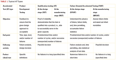
QT is certainly a must. Its objective is to prove that the reliability of the product is above a specified level. In Class I products, this level is usually measured by the percentage of failures per lot and/or by the number of failures per unit time (failure rate). The typical requirement is no more than a few percent failed parts out of the total lot (population). Testing is time limited. Industries cannot do without QT. QT enables one to “reduce to a common denominator” different products, as well as similar products, but produced by different manufacturers. QT reflects the state-of-the-art in a particular field of engineering, and the typical requirements for the product performance.
Today’s QT requirements are only good, however, for what they are intended – to confirm that the given device is qualified into a product to serve more or less satisfactorily in a particular capacity. If a product passes the standardized QT, it is not always clear why it was good, and if it fails the tests, it is often equally unclear what could be done to improve its reliability. It is well known that if a product passes QT, it does not mean there will be no failures in the field, nor is it clear how likely or unlikely these failures might be. Since QT is not failure oriented, it is unable to provide the most important ultimate information about the reliability of a product: the probability of its failure in the field after the given time in service and under the anticipated service conditions.
FOAT, on the other hand, is aimed at revealing and understanding the physics of the expected or occurred failures. Unlike QTs, FOAT is able to detect the possible
failure modes and mechanisms. Another possible objective of the FOAT is, time permitting, to accumulate failure statistics. Thus, FOAT deals with the two major aspects of the RE: physics and statistics of failure. While it is the QT that makes a device into a product, it is the FOAT that enables one to understand the reliability physics behind the product and, based on the appropriate PM, to create a reliable product with the predicted probability of failure. Adequately planned, carefully conducted, and properly interpreted FOAT provides a consistent basis for the prediction of the probability of failure after the given time in service. Well-designed and thoroughly implemented FOAT can facilitate dramatically the solutions to many engineering and business-related problems, associated with the cost-effectiveness and time-to-market. This information can be helpful in understanding what should be possibly changed in the design to create a viable and a reliable product. Almost any structural, materials or technological improvement can be “translated,” using FOAT data, into the probability of failure. That is why FOAT should be conducted in addition to, and, preferably, before the QT, even before the DQTs. There might be also situations when FOAT can be used as an effective substitution for any QT, especially for new products, when acceptable QT standards do not yet exist.
“Shifts” in the modes and/or mechanisms of failure might occur during FOAT, because there is always a temptation to broaden (enhance) the stress as far as possible to achieve the maximum “destructive effect” (FOAT effect) in the shortest period of time. AT conditions may hasten failure mechanisms (“shifts”) that are different from those that could be actually observed in service conditions. Examples are: change in materials properties at high or low temperatures, time-dependent strain due to diffusion, creep at elevated temperatures, occurrence and movement of dislocations caused by an elevated stress, or a situation when a bimodal distribution of failures (a dual mechanism of failure) occurs. Because of the possible shifts, it is always necessary to correctly identify the expected failure modes and mechanisms, and to establish the appropriate stress limits to prevent shifts. It is noteworthy that different failure mechanisms are characterized by different physical phenomena and different activation energies, and therefore, a simple superposition of the effects of two or more failure mechanisms is unacceptable: It can result in erroneous reliability projections.
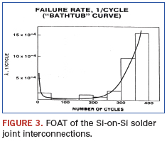
Burn-in (“screening”) testing (BIT) is aimed at the detection and elimination of infant mortality failures. BIT could be viewed as a special type of manufacturing FOAT (MFOAT). It is needed to stabilize the performance of the device in use. The rationale behind the BIT is based on a concept that mass production of electronic devices generates two categories of products that passed the formal QT: 1) robust (“strong”) components that are not expected to fail in the field, and 2) relatively unreliable (“weak”) components (“freaks”) that, if shipped to the customer, will most likely fail in the field.
BIT is supposed to stimulate failures in defective devices by accelerating the stresses that will most definitely cause these devices to fail. BIT is not supposed to appreciably damage good, “healthy” items. The bathtub curve of a device that underwent BIT is expected to consist of the steady state and wear-out portions only. BIT can be based on high temperatures, thermal cycling, voltage, current density, high humidity, etc. BIT is performed by the manufacturer or by an independent test house. Clearly, for products that will be shipped out to the customer, BIT is a nondestructive test.
BIT is expensive, and therefore, its application must be thoroughly designed and monitored. BIT is mandatory on most high-reliability procurement contracts, such as defense, space, and telecommunication systems; i.e., Class II and III products. Today, BIT is often used for Class I products as well. For military applications, BIT can last as long as a week (168 hr.). For commercial applications, BITs typically do not last longer than two days (48 hr.).
Optimum BIT conditions can be established by assessing the main expected failure modes and their activation energies, and from analysis of the failure statistics during previous BIT. Special investigations are usually required to ensure cost-effective BIT of smaller quantities is acceptable.
A cost-effective simplification can be achieved if BIT is applied to the complete equipment (assembly or subassembly) rather than to an individual component, unless it is a large system fabricated of several separately testable assemblies. Although there is a possibility some defects might escape the BIT, it is more likely that BIT will introduce some damage to the “healthy” product or might “consume” a certain portion of its useful service life: BIT might not only “fight” the infant mortality, but also accelerate the very degradation process that takes place in the actual operation conditions. Some BIT (e.g., high electric fields for dielectric breakdown screening, mechanical stresses below the fatigue limit) is harmless to the materials and structures under test, and does not lead to an appreciable “field life loss.” Others, although not triggering new failure mechanisms, might consume some small portions of the device lifetime. In lasers, the “steady-state” portion of the bathtub diagram is, in effect, not a horizontal, but a slowly rising curve, and wear-out failures occupy a significant portion of the diagram.
FOAT cannot do without simple and meaningful predictive models.5,6 It is on the basis of such models that one decides which parameter should be accelerated, how to process the experimental data and, most important, how to bridge the gap between what one “sees” as a result of the AT and what they will possibly “get” in the actual operation conditions. By considering the fundamental physics that might constrain the final design, PM can result in significant savings of time and expense and shed light on the physics of failure. PM can be very helpful also to predict reliability at conditions other than the FOAT. Modeling can be helpful in optimizing the performance and lifetime of the device, as well as coming up with the best compromise between reliability, cost-effectiveness and time-to-market.
A good FOAT PM does not need to reflect all the possible situations, but should be simple, should clearly indicate what affects what in the given phenomenon or structure, and should be suitable for new applications, new environmental conditions and technology developments, as well as for the accumulation, on its basis, of reliability statistics.
FOAT PMs take inputs from various theoretical analyses, test data, field data, customer and QT spec requirements, state-of-the-art in the given field, consequences of failure for the given failure mode, etc. Before one decides on a particular FOAT PM, they should anticipate the predominant failure mechanism, and then apply the appropriate model. The most widespread PMs identify the MTTF in steady-state-conditions. If one assumes a certain probability density function for the particular failure mechanism, then, for a two-parametric distribution (like the normal or Weibull one), they could construct this function based on the determined MTTF and the measured standard deviation (STD). For single-parametric probability density distribution functions (like an exponential or Rayleigh’s ones), the knowledge of the MTTF is sufficient to determine the failure rate and the probability of failure for the given time in operation.
The most widespread FOAT PMs are power law (used when the physics of failure is unclear); Boltzmann-Arrhenius equation (used when there is a belief that the elevated temperature is the major cause of failure); Coffin-Manson equation (inverse power law; used particularly when there is a need to evaluate the low cycle fatigue lifetime); crack growth equations (used to assess the fracture toughness of brittle materials); Bueche-Zhurkov and Eyring equations (used to assess the MTTF when both the high temperature and stress are viewed as the major causes of failure); Peck equation (used to consider the role of the combined action of the elevated temperature and relative humidity); Black equation (used to consider the roles of the elevated temperature and current density); Miner-Palmgren rule (used to consider the role of fatigue when the yield stress is not exceeded); creep rate equations; weakest link model (used to evaluate the MTTF in extremely brittle materials with defects), and stress-strength interference model, which is, perhaps, the most flexible and well substantiated model.
The Boltzmann-Arrhenius equation (model) 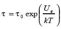 is most widespread in semiconductor reliability and underlies many FOAT related concepts. In this equation, τ is the MTTF, is the activation energy, k=8.6174 x 10⁻⁵eV/ºK is the Boltzmann’s constant, and is the absolute temperature. The equation addresses degradation and aging related processes. The failure rate is found as
 ![]() so that the probability of failure at the moment t of time, if the exponential formula of reliability is used, is
so that the probability of failure at the moment t of time, if the exponential formula of reliability is used, is  . If the probability of failure P is established for the given time t in operation, then this formula can be employed to determine the acceptable failure rate.
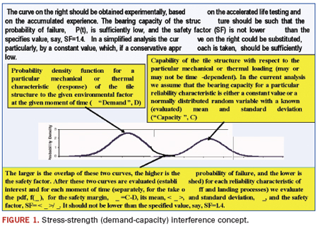
Stress-strength (demand-capacity) interference model (Figure 1) is the most comprehensive and flexible predictive model in reliability engineering.1 It enables one to consider the probabilistic nature of both the stress (demand, load) and strength (capacity) of the system of interest. If necessary and applicable, this model enables one to account for the time dependency of the demand and capacity probability distribution functions. The model might include Boltzmann-Arrhenius, Coffin-Manson and other FOAT models when addressing particular modes of failure.
Typical FOAT Procedure
Probabilistic DfR (PDfR) approach is based on the probabilistic risk management (PRM) concept, and if applied broadly and consistently, brings in the probability measure (dimension) to each of the design characteristics of interest.7-9 Using AT data and, in particular FOAT data, and PM techniques, the PDfR approach enables one to establish, usually with sufficient accuracy, the probability of the possible (anticipated) failure of the device for the given loading conditions and for the given moment of time, both in the field and during FOAT. After the probabilistic PMs are developed and the corresponding predictive algorithms are obtained, one should use sensitivity analyses (SA) to determine the most feasible materials and geometric characteristics of the design, so that the adequate probability of failure is achieved. In other cases, the PDfR approach enables one to find the most feasible compromise between the reliability and cost-effectiveness of the product.
When PDfR is used, the reliability criteria (specifications) are based on the acceptable (allowable) probabilities of failure. Not all products require application of PDfR – only those for which there is reason to believe the probability of failure in the field might not be adequate for particular applications. No one and nothing is perfect. Failures happen and the probability is never zero. The difference between a reliable and unreliable system (device) is in the level of the probability of failure. This probability can be established through specially designed, carefully conducted and thoroughly interpreted DFOAT aimed at understanding the physics of failure.
Usually product reliability is predicated on the reliability of its one or two most vulnerable (most unreliable) functional or structural elements. It is for these elements that the adequate DFOAT should be designed and conducted. SA are a must after the physics of the anticipated failure is established, the appropriate PMs are agreed on, and the acceptable probability of failure in the field is, at least tentatively, specified. SA should be carried out prior to the final decision to mass produce the product. DFOAT is not necessarily a destructive test, but is always a test to failure; i.e., a test to determine limits of the reliable operation and the probability that these limits are exceeded. A priori “probability-of-failure” confirmed by some statistical data (to determine the mean and STD values of the probability distribution of interest, but not necessarily the probability-distribution function itself) can successfully replace time and labor consuming a-posteriori “statistics-of-failure” effort(s).
Technical diagnostics, prognostication and health monitoring (PHM)11 could be effective means to anticipate, establish and prevent possible field failures. It should be emphasized, however, that PHM effort, important as it might be as part of the general reliability approach, is applied at the operation phase of the product and cannot replace the preceding FOAT, DfR, AM or BIT activities. The PDfR approach has to do primarily with the DfR phase of the product’s life, and not with Manufacturing-for-Reliability (MfR) efforts. BIT could be viewed, as has been indicated above, as a special and an important type of MFOAT intended to meet MfR objectives. BIT is mandatory, whatever DfR approach is considered and implemented.
Safety factor (SF) is an important notion of the PDfR approach. While the safety margin (SM), defined as the (random) difference Ψ = C – D between the (random) capacity (strength) and the (random) demand (stress) is a random variable itself, the SF is defined as the ratio 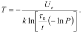 of the mean value
 ![]() of the SM to its STD
of the SM to its STD ![]() , and therefore is a nonrandom PDfR criterion of the reliability (dependability) of an item. It establishes, through the mean value of the SM, the upper limit of the reliability characteristic of interest (such as, stress-at-failure, time-to-failure, the highest possible temperature, etc.) and, through the STD of the SM, the accuracy, with which this characteristic is defined. For instance, for reliability characteristics that follow the normal law, the SF changes from 3.09 to 4.75, when the probability of non-failure (dependability) changes from 0.999000 to 0.999999. As one can see from these data, the direct use of the probability of non-failure might be inconvenient, since, for highly reliable items, this probability is expressed by a number that is very close to unity. For this reason, even significant changes in the item’s (system’s) design, which are expected to have an appreciable impact on its reliability, may have a minor effect on the probability of non-failure. This is especially true for highly reliable (highly dependable) items. If the characteristic (random variable) of interest is time to failure (TTF), the corresponding SF is determined as the ratio of the MTTF to the STD of the TTF.
, and therefore is a nonrandom PDfR criterion of the reliability (dependability) of an item. It establishes, through the mean value of the SM, the upper limit of the reliability characteristic of interest (such as, stress-at-failure, time-to-failure, the highest possible temperature, etc.) and, through the STD of the SM, the accuracy, with which this characteristic is defined. For instance, for reliability characteristics that follow the normal law, the SF changes from 3.09 to 4.75, when the probability of non-failure (dependability) changes from 0.999000 to 0.999999. As one can see from these data, the direct use of the probability of non-failure might be inconvenient, since, for highly reliable items, this probability is expressed by a number that is very close to unity. For this reason, even significant changes in the item’s (system’s) design, which are expected to have an appreciable impact on its reliability, may have a minor effect on the probability of non-failure. This is especially true for highly reliable (highly dependable) items. If the characteristic (random variable) of interest is time to failure (TTF), the corresponding SF is determined as the ratio of the MTTF to the STD of the TTF.
SF is reciprocal to the coefficient of variability (COV). While the COV is a measure of the uncertainty of the random variable of interest, the SF is the measure of certainty, with which the random parameter (stress-at-failure, the highest possible temperature, the ultimate displacement, etc.) is determined.
It is noteworthy that the most widespread FOAT models are aimed at the prediction of the MTTF only and directly. This means a single parametric probability distribution law, such as exponential distribution, is supposed to be used. The SF in this case is always SF=1.
As a simple example of the application of the PDfR concept, let us address a device whose MTTF during steady-state operation is described by the Boltzmann-Arrhenius equation, and assume that the exponential law of reliability is applicable. Solving this equation for the absolute temperature, we obtain:
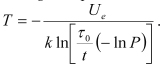
The given (anticipated) type of failure is surface charge accumulation, for which ![]()
the τ0 value obtained on the basis of the FOAT is τ0 = 2x10⁻⁵ hr., and the allowable (specified) probability of failure at the end of the device’s service time is, say, t = 40,000 hr. is Q = 10-5 i.e., it is acceptable that one out of 100,000 devices fails. With these input data, the above formula indicates that the steady-state operation temperature should not exceed T = 352.3˚K = 79.3˚C for the required reliable operation of the device, so that the thermal management equipment should be designed and its reliable operation should be assured accordingly. This elementary example gives a flavor of what one could possible expect from using a PDfR approach. Other, more in-depth, examples can be found in Refs. 8 and 9. The most general probabilistic approach, based on the use of probability density distribution functions and the cumulative distributions of the random characteristics of interest, is described by Suhir.10
It should be widely recognized and commonly accepted that the probability of a failure is never zero. It could be unacceptably low or unnecessarily high, but never zero. It should be further recognized that this probability could be predicted and, if necessary, specified, controlled and maintained at an acceptable level, and that the effort to establish such a probability does not have to be costly or time-consuming. One effective way to evaluate the probability of failure in the field is to implement the existing methods and approaches of PRM techniques and to develop adequate PDfR methodologies. These methodologies should be based mostly on FOAT and on a widely employed PM effort. FOAT should be carried out in a relatively narrow but highly focused and time-effective fashion for the most vulnerable elements of the design of interest. If the QT has a solid basis in FOAT, PM and PDfR, then there is reason to believe the product of interest will be sufficiently and adequately robust in the field. For superfluously robust, and perhaps, because of that, too costly products, application of FOAT can establish the unnecessary low probability of failure in the field.
The novel QT could be viewed as a “quasi-FOAT,” “mini-FOAT,” a sort-of the “initial stage of the actual FOAT.” Such a “mini-FOAT” more or less adequately replicates the initial non-destructive, yet full-scale, stage of the full-scale FOAT. The duration and conditions of such “mini-FOAT” QT should be established based on the observed and recorded results of the actual FOAT, and should be limited to the stage when no failures, or limited and “prescribed” (anticipated) failures, are observed, and that “what one sees” is in accordance with “what one got (observed)” in the actual full-scale FOAT. PHM technologies could be of a significant help in this effort. “Canaries,” for instance, could be concurrently tested to make sure the safe limit is not exceeded.
We believe that such an approach to qualify devices into products will enable industry to specify, and the manufacturers to ensure, a predicted and adequate probability of failure for a device that passed the QT, and will be operated in the field under the given conditions for the given time. FOAT should be thoroughly implemented, so that the QT is based on the FOAT information and data. PDfR concept should be widely employed. Since FOAT cannot do without predictive modeling, the role of such modeling, both computer-aided and analytical (“mathematical”), in making the suggested new approach to product qualification practical and successful. It is imperative that the reliability physics that underlies the mechanisms and modes of failure is well understood. No progress in coming up with an adequate level of the reliability of a product in the field can be expected if the physics of failure is not understood well. Such an understanding can be achieved only provided that FOAT, PM and PDfR efforts are implemented.
Minimizing Field Failure Risk Steps
- Develop an in-depth understanding of the physics of possible failures. In this respect, there needs to be a continuous effort to ensure and improve the predictability of models; i.e., models must accurately replicate the physics of the problem comprehensively and should be well supported by good materials characterization.
- Validate models through use of relevant experimental techniques such as in-situ sensors, photo-mechanics, etc.
- Neither failure statistics, nor the most effective ways to accommodate failures (such as redundancy, troubleshooting, diagnostics, prognostication, health monitoring, maintenance), can replace an understanding of the physics of failure and good (robust) physical design.
- Assess likelihood (probability) that the anticipated modes and mechanisms might occur in service conditions and minimize likelihood of a failure by selecting the best materials and best physical design.
- Understand and distinguish between different aspects of reliability: operational (functional) performance, structural/mechanical reliability (caused by mechanical loading) and environmental durability (caused by harsh environmental conditions).
- Distinguish between materials and structural reliability and assess the effect of mechanical and environmental behavior of the materials and structures in the design on product functional performance.
- Understand the difference between requirements of qualification specifications and standards, and actual operation conditions. In other words, understand the QT conditions and design the product not only so it would withstand operation conditions on a short- and long-term basis, but also to pass QT.
- Understand role and importance of FOAT, the PDfR and conduct PM whenever and wherever possible.
Ephraim Suhir, Ph.D., is Distinguished Member of Technical Staff (retired), Bell Laboratories’ Physical Sciences and Engineering Research Division, and is a professor with the University of California, Santa Cruz, University of Maryland, and ERS Co.; suhire@aol.com.
Ravi Mahajan, Ph.D., is senior principal engineer in Assembly Pathfinding, Assembly and Test Technology Development, Intel (www.intel.com); ravi.v.mahajan@intel.com.
References
1. E. Suhir, “Applied Probability for Engineers and Scientists,” McGraw Hill, New York, 1997.
2. E. Suhir, “How to Make a Device into a Product: Accelerated Life Testing, Its Role, Attributes, Challenges, Pitfalls, and Interaction with Qualification Testing,” E. Suhir, CP Wong, YC Lee, eds. “Micro- and Opto-Electronic Materials and Structures: Physics, Mechanics, Design, Packaging, Reliability,” Springer, 2007.
3. E.Suhir, “Reliability and Accelerated Life Testing,” Semiconductor International, February 1, 2005.
4. A. Katz, M. Pecht and E. Suhir, “Accelerated Testing in Microelectronics: Review, Pitfalls and New Developments,” Proceedings of the International Symposium on Microelectronics and Packaging, IMAPS, Israel, 2000.
5. E. Suhir, “Thermo-Mechanical Stress Modeling in Microelectronics and Photonics,” Electronic Cooling, vol. 7, no. 4, 2001.
6. E. Suhir, “Thermal Stress Modeling in Microelectronics and Photonics Packaging, and the Application of the Probabilistic Approach: Review and Extension,” IMAPS International Journal of Microcircuits and Electronic Packaging, vol. 23, no. 2, 2000.
7. E. Suhir and B. Poborets, “Solder Glass Attachment in Cerdip/Cerquad Packages: Thermally Induced Stresses and Mechanical Reliability,” Proceedings of the 40th ECTC, May 1990; see also: ASME Journal of Electronic Packaging, vol. 112, no. 2, 1990.
8. E. Suhir, “Probabilistic Approach to Evaluate Improvements in the Reliability of Chip-Substrate (Chip-Card) Assembly,” IEEE CPMT Transactions, Part A, vol. 20, no. 1, 1997.
9. E. Suhir, “Probabilistic Design for Reliability (PDfR),” ChipScale Review, vol. 14, no. 6, 2010.
10. E. Suhir and R. Mahajan, “Probabilistic Design for Reliability (PDfR) and a Novel Approach to Qualification Testing,” IEEE CPMT Transactions, submitted for publication.
11. M.G. Pecht, Prognostics and Health Management in Electronics, John Wiley, 2009.

Press Releases
- Zollner Puts a New Mechanics Building into Operation
- Changes in Incap’s Management Team: Incap updates its leadership model to support its growth strategy
- Niche Electronics Celebrates Completion of Florida Expansion
- Microscreen Names Nik Thomas Director, Expands Leadership Role Amid Continued Organizational Growth