

The world’s unsung solder supplier is building a business for the ages.
A few minutes before noon, the cafeteria starts to fill with dozens of workers, blue collar and white, some in business casual wear, others in their factory blues. The volume begins to rise, a cacophony of sounds and languages, English and French, spoken in an endless variety of flavors.
Within an hour, the room falls quiet again as the staff resumes its roles inside the vast manufacturing facility that doubles as the global headquarters of AIM.
The melting pot culture of AIM is probably the least well-known aspect of what might be the least well-known large solder supplier in the electronics industry today.
Founded in 1936 as American Iron and Metal, the company has its roots in metals recycling and reclaim. Now a subsidiary, AIM’s solders business was formed 22 years ago, and was spun out in 2007. It maintains the same ownership as AIM, though each unit is a separate legal entity. Ricky Black, the 40-something grandson of the founder, heads AIM Metals and Alloys, which has manufacturing sites in Canada, China, the US, Mexico, Hong Kong, Spain, Italy and Australia.
The Montreal headquarters is situated on a massive campus that stretches more than two miles from front to back, where a set of rail sidings slides right up to the door. While Montreal is considered home to the company’s extensive bar, wire and solder paste operations, AIM also maintains mixing and blending operations in the US and Hong Kong.
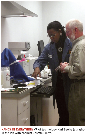
Heading up the technology side is Karl Seelig, a 30-year veteran of electronics materials. Seelig came aboard in 1988 to help launch the electronics solders business. His imprint on the company’s solder product lines can be seen everywhere, from the formulations to the equipment used to make the powders.
The plant tour begins in the core wire area. There, workers start with 15mm or smaller wire, which is then reduced in diameter using an extrusion press (AIM has five on site). Core wire operations also take place in Mexico, China and Europe. (Because of the large volumes, AIM makes core wire in fewer places than other solder types.)
We pass the metal castings area, where three continuous casters labor in a humidity- and temperature-controlled room pressurized for fume extraction.
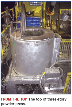
From there, we walk past several drums of butyl carbide to the lab where AIM makes its paste medium. Using dedicated mixers for water-soluble, cored wire and no-clean, operators weigh the bucket to get the precise weight; even a slight deviation could ruin a batch. The powder press is truly impressive: Molten metal pours into a dish; solder falls into the chamber, then onto a screen, then to the atomizer. It’s a three-story process. An oxide “skin” forms; a thin skin is needed on every layer. Powder is exposed to atmosphere for about one hour, then vacuum packed with gas and labeled. Yields are about 70%, very high for electronics grade solders. Paste is made in a 45% RH dry room. Each lot is tested for corrosion, electromigration, thermal cycling and SIR, among others. “Everything has to be tested,” Seelig notes. While AIM is a leading supplier of bar solder, many would be surprised at the volume of its paste business. Combined, the total revenues from the two segments easily place AIM among the five largest electronics solder suppliers in the world. “The ratio of bar to paste is lower than five years ago. The industry doesn’t realize how much we do in paste. Maybe it goes with our understated personalities,” deadpans Black.
AIM uses standard blenders with automatic controls designed to be programmed, but that cannot be adjusted by operators. All paste is made to order, and alloys and formulas tend to be the outgrowth of face-to-face discussions between Seelig and AIM’s marketing staff with OEMs and EMS firms. Inventories are kept low, with a few emergency stocks of common types.
The liquid flux is made in an explosion-free room. All flux chemistry is designed and made in Montreal. (Chemistry is the main expense in R&D; the cost to develop an alloy is relatively low. Changing it, however, is a long, drawn-out process, Selig allows.) We also see a small SMT epoxy room with a mill for different pigments.
The ISO 9001 registered, ISO 17025 compliant Quality Assurance lab is bright and clean, with a new Thermo Fisher Quant x-ray and a Thermo Electron 3460 metals analyzer, among other gear. AIM performs arc-spark testing to check for all standard impurities, with tests run to IPC specifications and multiple others. More than 1,000 samples per month are analyzed. Montreal is one of three company labs; others are in China and Mexico.
Most customers look at particle distribution, so that’s a standard item for the lab review. In-house software assesses some 45,000 particles, checking width, length, diameter and so on. Every tank is sampled multiple times; then a chemical analysis is performed to ensure the barrel is satisfactory. All electronics grade solder is made from virgin metal. Reclaimed material is reserved for industrial use only.
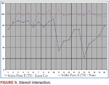
The applications lab features a DEK printer, Quad placement machine, Heller 1500 reflow oven, CRT CRX-1000 x-ray and Koh Young 3020T SPI. Tests are conducted using electroform, lasercut and nanostencils.
R&D is performed in Montreal, Rhode Island and China, while tech support centers are based in India, Singapore, Philippines, Mexico, North America, Europe and China. In Montreal, AIM maintains separate labs for various types of paste, cored wire and testing, and each chemist has their own specialty. (Similar labs are set up in Mexico and China.) AIM also provides adhesives, but they are not big sellers.
All paste is made to order. Inventories are kept low, with a few emergency stocks of common types. Prior to shipping, every package is scanned with an XRF to ensure it’s the right formulation.
Supply Local, Supply Global
Over the past 10 years, supplying solder has been a tricky business. The RoHS Directive permanently rerouted the industry direction, causing a disruption in pricing that is felt to this day. Solder is, of course, one of the lower items on the bill of materials totem pole. Unlike most raw material prices, precious metals are in a sustained period of inflation. Despite this – because of it, in fact – solder vendors do not capitalize. Indeed, most find the higher metal prices make their market more treacherous: Customers sometimes balk at paying more; vendors pay cash for raw metal, and it may take 100 days or more to turn that metal into solder and get paid by a customer, so the higher raw metal prices increase the supplier’s risk and cost of doing business; the cost to reclaim dross increases.
“Higher metals prices don’t necessarily work in our favor,” says Black. “Take SAC: The silver price is more than the tin,” even though silver is a minor element by weight in the SAC formula. “We don’t make our money on the metal, but on the things we do to it.”
AIM not only does a lot of “things” to the metal, it does those things in a lot of places. Perhaps owing to its aforementioned understated approach, AIM is considerably larger than most in the industry realize. Its breadth is a byproduct of its supply strategy, which assumes even larger accounts want local service. “If we didn’t supply locally, we wouldn’t be able to supply globally. It’s a consumable product; people run out,” Black explains. “The way to do that is to have your own facilities.”
With 12 sites up and running, AIM doesn’t see an end yet in sight. Black says he’s “almost convinced” more facilities will be erected, although he doesn’t yet know where. “It also depends on what the market wants to consume,” Seelig adds, pointing to the logistics of the supply chain. “We can’t ship alcohol-based or water-based flux or bar solder via air freight.”
The channel plays a large role in the company’s success, Black says. “You need to have the distributors to make sales. Customer orders tend to ebb and flow, and they need quick deliveries. [Solder] freight is high relative to the value and margin of the product, so it forces you to have local stock.” AIM prefers distributors that are hands-on and seen as adding value with technical expertise. In Europe, South America and Asia, it tends to use a single distributor per country.
While some competitors focus on landing large accounts, AIM doesn’t have a customer larger than 1.5% of its annual sales. Instead, it prefers companies that would rely more heavily on AIM’s technical know-how. “We try to find niches that are less competitive,” says Black. “There’s a lot of opportunity in smaller and mid-sized companies, where we can provide expertise to their product. The number of engineers and technicians per line has shrunk. We are now where companies turn for engineering applications help.”
Family Matters
If one were to survey the solder landscape, two types of companies would emerge. On one end are divisions of large multinational corporations, such as Cookson’s Alpha unit, Senju, Henkel and Kester. On the other end are the family-run businesses, of which there are dozens. AIM falls into the latter, although its size clearly outstrips not only others of its genre but most of the publicly traded units as well. Although the Black name is not on the door, the family’s history is inescapable and informs his vision.
A very self-aware individual who says he had “no guarantee” of ownership in the company, Black says he recognized early in his career that he would have to earn the respect of his coworkers. “I had to earn the trust and be self-conscious of how my words and actions would be perceived within the company. There are expectations, and I set high ones for myself. It’s about accomplishment, not money.
“Sometimes when a family gets too successful, and the founder retires, the work ethic goes with them. Passion sets a good example and people pick up on that. It’s very important for the company to maintain the culture that got us here. It must get transferred to the people who make the day-to-day decisions.”
Black came to the business not as a technologist but from law school. Although he acknowledges the experience would be useful, he does not see the lack of a technical degree as a drawback. In fact, he suggests his background may make him more open-minded to his staff’s opinions. “I don’t have a technical background. And I’m running a business that is heavily dependent on that. Maybe there’s a certain intangible effect. I’m much more interested in hearing what people think and can do.
“I don’t think of solder as different from other businesses. A business decision is a dollars and cents issue. When it comes to business decisions, I don’t need to understand metallurgy to make that decision. I’m in as good a position as anyone to make decisions. I am heavily reliant on our people for technical solutions.”
As if to reinforce a culture of creative thinking, Black chooses not to align departments to budgets, asserting better due diligence and quality as a result. “Things flow better. One has to be something of an entrepreneur and operate without guidance. People who need committee meetings don’t work out well here.”
Brand Power
While Black has been charting his own path, over the years AIM too has attempted to develop its signature label. In the 1990s, it made one of the few attempts to attach a name to the otherwise endless list of solder designations. Branded as CASTIN, the patented tin-silver-copper-antimony alloy never met with mass board-level appeal, but has found a niche in BGA balls used in most handhelds.
Although a developer by preference, AIM did make the leap in 2005 as a licensee of Nihon Superior’s SN100C alloy. “The license with Nihon is a unique situation,” explains Black. “It helped launch AIM as a player in North America. There was a lot of testing and data available for SN100C, and it was winning over a lot of the European and Asian markets. So now we are part of a global organization with data and branding.”
AIM, whose license covers North America and China, isn’t just manufacturing and distributing the solder, says Black. “We also injected quite a bit of technology to the cored wire.”
Rebounding from the 2008-09 recession, 2010 turned out to be a record year for AIM and SN100C. But while Black extols the virtues of working with Nihon Superior, he recognizes AIM is at its core a manufacturer.
“Brand is a huge factor in electronics, and we’ve spent a long time building a brand. And we have a way to go to get where I think we need to be. David Suraski is our sales and marketing face. Karl Seelig is our technical face. It’s important for people to associate us. Customers get comfortable with long-term tenure. You don’t want to ignore the value of your brand; it should outlive your representation. Customers confirm these relationships to different people. Everyone’s in sales.”
Throughout our two-day visit, Black reiterated his desire to build a business structure that is flat and endures. In doing so, he allows, he is borrowing from his father’s vision. “Herbert Black’s legacy is to build something lasting. I don’t want to get disconnected from what happens in the company. The guy who pours the metal is two layers from me. That comes from my dad and our family history.
“Ethics, moral and principles: They have to come first. Be upfront. Your mark on the world is the impact and effect on the people around you, not the building you put up or the company you worked in.”

Mike Buetow is editor in chief of CIRCUITS ASSEMBLY (www.circuitsassembly.com); mbuetow@upmediagroup.com.
Developing a recipe that will satisfy both boards.
Dual-lane reflow ovens have been available for years, permitting two boards to be run at the same time in parallel. Until recently, circuit board manufacturers have been limited to processing the same boards or boards with like mass in each of the lanes, but dual-lane reflow ovens with independent lane speeds now make it possible to run boards with larger differences.
Now we have the ability to run different speeds in each lane; it is the process engineer’s responsibility to develop the recipe that will satisfy both boards. The following gives practical insight into a method to obtain this recipe.
To begin, understand factors that affect the transfer of thermal energy from the heater in a convection oven to the board. In most cases reflow oven fans push gas (air or nitrogen) across a heated electric coil to increase its temperature. Then the hot gas is distributed to the product through a series of holes in an orifice plate, as shown below. The equation that describes the transfer of energy from the hot gas to the board is well known
q = a · t · A · ∆T Eq. 1
where
q = the thermal energy being transferred to the board
a = the heat transfer coefficient of the board and components
t = time the board is in the heat
A = the surface area the heat sees
∆T = the temperature difference between the gas (convection) and the board
When we move the board parameters to one side of the equation and the oven parameters to the other side, we get
q = t · ∆T Eq. 2
a · A
By introducing a heavier or lighter board to the equation, the a and A factors change. Thermal energy absorbed by the board (q) then adjusts so the equation remains balanced. This change in thermal energy (q) results in a different board temperature. To maintain the board temperature, we must change either the zone set points (∆T) or belt speed (t).
Application. When running a new board in a single-lane oven, we adjust the profile by modifying the set points (∆T) and/or the belt speed (t) to obtain the correct profile. But if two different boards are run in a dual-lane oven, we can only change the belt speed because both lanes see the same temperature (set points).
In August 2009, a report published by BTU1 showed how changing the belt speed, zone set points and convection rate affected a solder reflow profile. It looked at how the furnace settings affected the peak temperature, time above liquidus and uniformity of two SMT boards. This new study varied the belt speed from 30 IPM to 60 IPM on a 75 gm, 360 g and 520 g board with eutectic and Pb-free recipes on a Pyramax 150 12-zone nitrogen reflow oven. The change in peak temperature, time above liquidus and soak time of each combination was recorded.
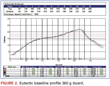
Eutectic recipe. The first step in the trial was to establish a baseline recipe that produced a standard ramp-soak-spike profile with the 360 g board at 45 IPM (Figure 2). The peak temperature was targeted at 220°C, time above liquidus (TAL) at 60 sec., and the time between 140° and 170°C at 70 sec.
Next the belt speed was changed in steps of approximately 5 IPM to a maximum and minimum of 15 IPM from the starting point on the three boards. We recorded the new peak temperature, TAL and soak time for each step. The results are shown in Figures 3-5.
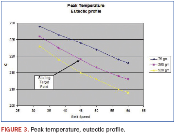
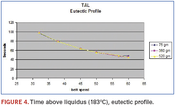
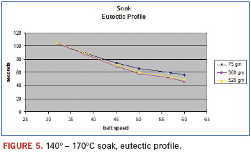
As expected, the board weights had an influence on the peak temperature with the heavier board being 7° to 10°C colder than the light board. But there was little difference in TAL or soak time between the boards.
The belt speed change affected all three parameters. The TAL and soak time were changed by almost 50 sec., and the peak temperatures varied by around 15°C.
Practical application. We then applied the data to the real-life situation of running two different boards in the same oven. We started with the 360 g board in one lane and wanted to run the 75 g board in the other. Figure 3 revealed we needed to increase the belt speed to 58 IPM (see Figure 6) to maintain the same peak temperature on both boards. Meanwhile, Figures 4 and 5 told us that the TAL and soak of the 75 g board would shorten to approximately 45 and 55 sec. with the 58 IPM belt speed.
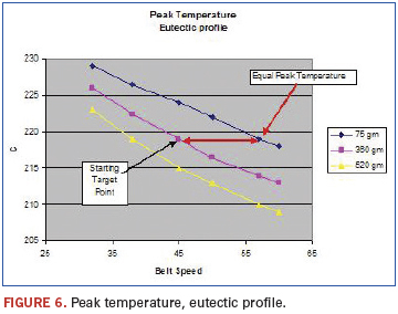
Likewise, if we wanted to run the 520 g board with the 360 g board zone temperatures, we needed a belt speed of 38 IPM to maintain the peak temperature. The resulting TAL would be 80 sec. and soak would be 85 sec.
If we could accept the new TAL and soak times, the new second board belt speed would work. If we could not accept the new TAL or soak, we would need to accept a different peak temperature on the new board or try different set points on both boards.
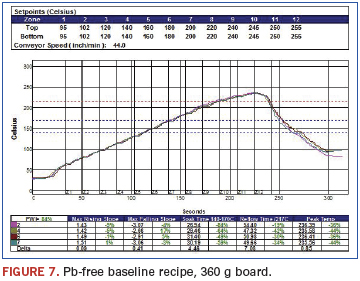
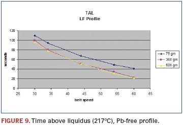
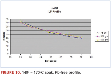
Pb-free recipe. Next we repeated the data acquisition for a Pb-free profile. We established the baseline recipe for a Pb-free ramp-to-peak profile on the 360 g board at 44 IPM (Figure 7). The peak temperature target was 240°C, with a time above the 217°C liquidus of 60 sec. Since there is usually little or no soak on Pb-free profiles, we monitored the time between 140° and 170°C in the event the soak becomes a consideration in the future.
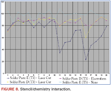
We then followed the procedure used with the eutectic profile and varied the belt speed ±15 IPM from the starting point. The new peak temperature, TAL and soak time were recorded for the various belt speeds with each of the three test boards. The results are shown in Figures 8, 9 and 10.
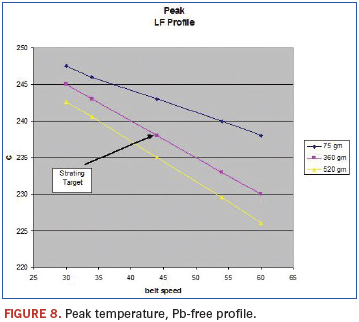
The board weights had the same effect on the peak temperature that we had with the eutectic solder profile. At the lower belt speeds, the difference between boards was about 7°C, and at the faster speeds, it was close to 13°C. But unlike the eutectic profile, where the mass did not affect the TAL or soak time, the TAL was about 20 sec. longer with the lighter 75 g board. (This most likely was due to the ramp to peak profile shape.)
When the belt speed was varied, all three parameters changed as in the eutectic profile. The TAL changed by 80 sec.; the soak time changed by 20 sec., and the peak temperature changed by around 15°C.
The charts gave us the same information as with the eutectic profile. The peak temperature chart (Figure 8) tells us that if we were using the recipe we established for the 360 g board, and we wanted to run a 75 g board in the parallel lane, we would need to increase the belt speed to 60 IPM. Figures 9 and 10 tell us that the TAL and soak of the 75 g board with a belt speed of 60 IPM would be approximately 40 and 20 sec.
Likewise, we could run the 520 g board with the 360 g board recipe at 39 IPM to maintain the peak temperature. The resulting TAL would be 62 sec. and soak would be 32 sec. If we could accept the change in TAL and soak, changing the speed would work in these cases.
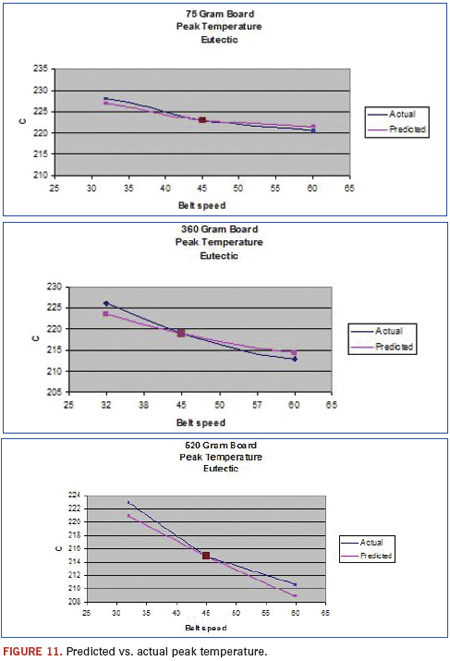
Predictive software. After numerous profiles, it was realized that a method was needed to shorten the time it took to obtain the data for these charts. The data in the first trials were close to linear over the speed range; therefore, our first thought was to obtain the base profile on the primary board and then run two profiles on the secondary board with the same zone set points and belt speeds of ±15 IPM. We could then connect the dots, draw a parallel line, and come up with a new belt speed for the secondary board. This would require only three profiles to establish the preliminary belt speed estimate.
Next we wondered if predictive software such as KIC Navigator could be used to forecast the profile. We had used a KIC Explorer to obtain the original profiles for the trial, so it was an easy step to see what the KIC Navigator would predict if told to change just the belt speed on the Pb-free baseline runs for each board. The software predicted peak temperatures that were within 2° to 3°C of what was actually measured. The peak temperature predicted results vs. actual for the three boards, shown in Figure 11.
Conclusion
With a little understanding and work, a process engineer can develop the data to help find a recipe that will allow them to establish the set points and belt speeds for dual-lane dual-speed reflow ovens. It can be done in multiple runs with actual belt speed changes or as few as two runs by using predictive software. It will also help determine the extreme cases where the boards are too different to be run on a dual-lane dual-speed oven. In all cases, the engineer needs to confirm the results by profiling the actual boards at the belt speeds they determined would be best.
The great lesson is that after the first profiles are optimized on the reflow oven, much of the remainder of the work can be done at the engineer’s desk without tying up the production equipment.
A Common Recipe
Obtaining the baseline recipe for the primary board is an important step in the process of developing recipes for dual-lane dual-speed reflow ovens. In some cases ptimizing the set points for the peak temperature, TAL and soak time for the primary board could result in profile parameters that are unacceptable for the second board. When this happens, the process engineer needs to identify a different primary board recipe and try again. We asked ourselves if there was a way to combine the profile data from the two boards to find a common recipe that would allow us to make a midpoint tradeoff of the TAL, soak and peak temperature for both boards.
A discussion with KIC revealed an applications note describing a method of developing a common recipe for mixed boards that required only a belt speed change on a single process line to save changeover time.2 The note describes running two boards in the oven at the same time with TCs on both products. The software then suggests a common recipe that minimizes the PWI on both boards. It can even utilize different profile requirements for each TC or, in this case, board.
Applying the technique of running two boards at the same time to obtain a baseline recipe for the dual-lane dual-speed oven seems to have benefits for the first step. Although both boards might not be in specification, the error would be divided between the two boards, and belt speed changes could be done on each lane. The only problem would be to run two boards through the oven at the same time and not have the TCs tangle in the edge rail hangers, but this can be overcome by running the boards, one behind the other in one lane, with the appropriate board supports.
References
1. Fred Dimock, “Oven Adjustment Effects on a Solder Reflow Profile,” CIRCUITS ASSEMBLY, August 2009.
2. KIC application notes, Developing Common Reflow Oven Recipes for Mixed Production Lines Using the KIC Navigator, kicthermal.com.
Fred Dimock is manager, process technology at BTU International (btu.com); fdimock@btu.com.
Paste chemistry and rheology have a more profound effect on release than previously thought.
PCB assemblers are reaching the limits of Type 3 solder paste. The goal of this study was to determine the impact on solder volume deposition between Type 3, Type 4 and Type 5 SAC 305 alloy powder in combination with stainless steel laser cut, electroformed and the emerging laser cut nano-coated stencils. Leadless QFN and µBGA components utilizing optimized aperture designs were the focus of the test. The test procedure evaluated pause-to-print and volume transfer efficiencies on 20 boards over an 8 hr. period. A concurrent study using the same boards evaluated the impact of powder particle size on voiding of QFN ground pads testing 18 different aperture designs.
With components such as QFNs, µBGA and 01005 passive devices with small lead areas and corresponding pad geometries, it is possible that Type 3 solder paste is too large to permit accurate and repeatable solder paste deposition. This issue impacts all facets of the manufacturing process, not just the solder paste used when assembling such components to a PCB.
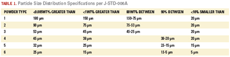
It has been an assumption that the smallest aperture solder paste can pass through repeatedly is five times the largest sphere size of the metal powder. In Type 3 powder, the average sphere size is 45 µm, with allowances to 53 µm. Theoretically, an 0.0089" aperture is the minimum aperture that can be printed with Type 3 solder paste (Table 1).
Moreover, there are myriad aspects when considering the proper stencil design for a given assembly. For the purposes of this experiment, the goal was to minimize the variables to ensure the results obtained reflected the aspects under our control.
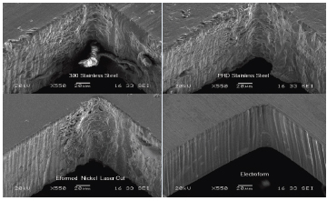
Electroformed nickel stencils (e-form) provide the taper, wall smoothness and lubricity that lend to the best paste release characteristics. However, they are significantly more expensive than traditional laser-cut, electropolished stencils and may not be as readily available. Laser-formed stencils are a relatively new option. These stencils are cut using upgraded lasers in combination with high nickel content foil materials. They represent an improvement over standard laser-cut stencils at a lower cost than e-form. These two technologies were used in this experiment.
Finally, an emerging technology termed “nano-coating” has been made available in some markets. This technology and process are largely proprietary, but the process is described as:
“After the brushing and cleaning operation, the laser cut stencil runs through a special designed coating machine. The inorganic coating is dissolved in a very environmentally friendly solvent. The constant thickness of the nano coating is the key technology of the coating process. In a continuous furnace the coating is dried out, and a multiple stage heat treatment polymerizes the dry inorganic layer. In the same equipment, a chemical reaction with an organic chemical is carried out to provide the hydrophobic anti-adhesion properties.”1
The main function of the coating is to reduce the surface tension between the paste and stencil material. A reduction in surface tension creates a non-stick surface, facilitating better paste release, resulting in more consistent paste volume deposits and less residual paste in the aperture, thereby aiding in volume deposition accuracy in subsequent print cycles. A stencil identical to the laser-formed stencil was nano-coated using Laser Job in Germany and included in the experiment. Aperture designs were optimized for paste volume deposition.
Stencil specifics:
- PHD stainless steel.
- Thickness tolerance is +/-3 or 4%.
- Hardness is 370 HV min.
- Flatness: max. edge wave 1.5 mm and max. center wave 0.50 mm.
- Grain size typically 10-25 µm.
A fiber diode type laser was used to cut the stencils. It was a gantry-style motion system with 10 nm resolution and 0.5 µm repeatability. Operation and connections were auto-focus. The laser was a 150W Class I fiber laser system, air-cooled, with permanent align beam delivery and compressed air cutting.
Experiments were conducted at AIM’s Montreal Production Simulation facility using a DEK 265 GS printer, a Quad QSP IV placement machine, a Heller 1500 reflow oven and Koh Young KY3020T SPI.
The lab process was as follows: The temperature was 22° to 23°C with 24 to 26% RH. A 12" squeegee was used, with a squeegee pressure of 0.8 lb. and speed of 1"/sec.
Materials used included:
- No-clean SAC 305 T3 Solder Paste A.
- No-clean SAC 305 T4 Solder Paste B.
- No-clean SAC 305 T5 Solder Paste C.
- No-clean SAC 305 T3 Solder Paste D (modified for better printing).
- No-clean SAC 305 T3 Solder Paste E.
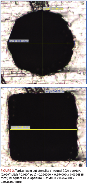
- BGA stencil (0.005" laser cut) (Figure 3).
- QFN LGA Stencil (0.005" laser cut, 0.005" electroform, 0.005" nano-coat, 0.005" nano-coat laser cut, 0.005" proprietary coated laser cut).
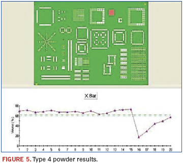
Test method. The test method was developed to simulate a low-to-mid-volume production environment with pauses between print cycles at regular intervals. Volume and height measurements were taken immediately following completion of printing of the test board. Boards 1 to 5 were printed and measured, and the process paused for 30 min. Boards 6 to 10 were printed and measured, and the process paused for 60 min. Boards 11 to 15 were printed and measured, and the process paused for 90 min. Boards 16 to 20 were printed and measured (Figures 4-7).
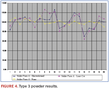
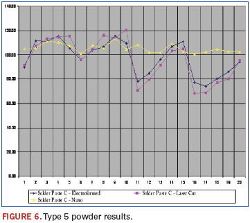
Solder paste/chemistry observations. The results indicate that neither mesh size nor stencil type have a significant impact on the volume of paste released from the stencil aperture (uncoated stencil). The paste deposit may have a different appearance visually between types, but the critical measure of volume is unaffected.
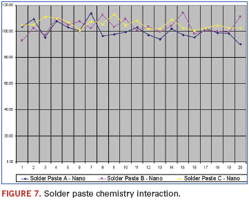
This was somewhat surprising, as it was believed that e-form stencils and paste manufactured with Type 4 powders would provide the most consistent paste release characteristics. To further develop the data, an additional variable was introduced to determine the impact of paste chemistry on the deposition volume. A developmental solder paste material was introduced to the experiment for comparison and the following results obtained (Figure 8).
As evidenced by the data, paste chemistry/rheology has a more profound effect on release characteristics than either stencil or powder mesh size (Figure 9).
The impact of nano-coating on the release characteristics of solder paste from stencil apertures was the single biggest variable in improving release volume consistency.
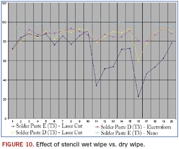
Testing was performed with the addition of a solvent deemed compatible with the paste chemistry in use to assess the impact on the release characteristics. It was found the addition of a solvent to the underside wipe cycle of a stencil printer has a moderately positive effect on the release volume of the paste from the stencil aperture (Figure 10).
Conclusions
The variables that have the most significant impact on paste release on fine-pitch apertures are listed below in order of significance:
- Stencil type (nano).
- Paste chemistry/characteristics.
- Stencil wipe (solvent wipe compatible with paste).
Nano-stencil technology has a profound impact on the performance of paste release. This is an emerging process with many competing technologies under development.
Following nano-coating, paste rheology and chemistry are areas of continued development by solder paste manufacturers. Pb-free solder pastes are still relatively new in comparison to their leaded predecessors, and continued improvements are expected as the technology matures.
The introduction of solvent to the printer stencil wipe process is a relatively inexpensive process improvement with few negative side effects, assuming the material is deemed compatible with the solder paste in use. Based on these findings, it can be inferred that stencil design and materials have a far greater impact on release characteristics than paste powder mesh size.
Karl Seelig is vice president, technology and Tim O’Neill is Northeast regional sales manager at AIM Solder Products (aimsolder.com); kseelig@aimsolder.com.
A rising tide lifted most – but not all – ships.
The electronics manufacturing industry will remember 2010 for many reasons: rampant component shortages (and the rise of counterfeits), the tight financial markets and tense end-market conditions.
But mostly, it will remember 2010 for the long-awaited recovery.
EMS shook off the doldrums of 2008-09, demonstrating tremendous resilience and yes, patience, as demand easily outstripped supply throughout the calendar year.
It also showed it remembered the lessons from 1999 to 2001, where unprecedented OEM demand led to acquisition sprees and six-month order lead times. It took two years for that hangover to end.
Not this time.
Expansion occurred, of course, but it was targeted. Even Foxconn, which announced or opened several sites in China during 2010, didn’t bring on capacity so much as it relocated it inland from the Shenzhen area, where inflation and negative attention coupled with a parade of worker deaths made the “Walled City” environs even more uncomfortable than usual. Most followed the lead of companies like Zollner, which expanded two plants in China, but left the rest of its footprint as is.
Acquisition activity was also held in relative check. The big deal of the year was Sanmina-SCI’s purchase of Breconridge (No. 48 in last year’s revised Top 50). Smaller deals abounded, but were generally on the order of the MC Assembly’s pickup of Chase Corp.’s EMS operations or ElectronicNetwork’s snatching of Görmiller from bankruptcy, tidy deals that were quickly accretive and added 10 to 15% in revenue to the balance sheet but didn’t do much insofar as moving the needle on the CIRCUITS ASSEMBLY Top 50 chart.
Falling off the Circuits Assembly Top 50 this year was Hitachi Computer Products, as expected, as the Oklahoma site ceased taking outside orders to concentrate on its parent company’s production needs. Jumping in were a handful of firms that were unintentionally omitted in 2010. They include Japan’s UMC Electronics and Hong Kong’s PC Partner, Topscom and Fittec.
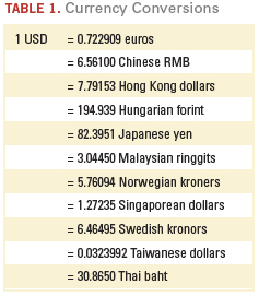
Currency fluctuations did not have a profound effect on this year’s results, as most of the major currencies were fairly stable with last year, trading in a band of 3 to 5 percentage points. The exception was the Japanese yen, which had fallen 9.5 points against the dollar from Feb. 1, 2010 to Feb. 1, 2011, the date used for the conversions (Table 1).
While the big clearly got bigger, the middle class acquitted itself nicely (Table 2). No. 30 Eolane finished 2010 with 268 million euros in revenue, up 72% from 156 million euros last year. No. 19 Fabrinet (the early leader for 2011’s CIRCUITS ASSEMBLY EMS Company of the Year) shot up 72% as well on demand for optical networks. No. 38 Neways was up 27%. In North America, military/industrial suppliers On Core and Victron each grew around 20%.
[Ed.: To enlarge the table, right-click on it, then click View Image, then left-click on the table.)
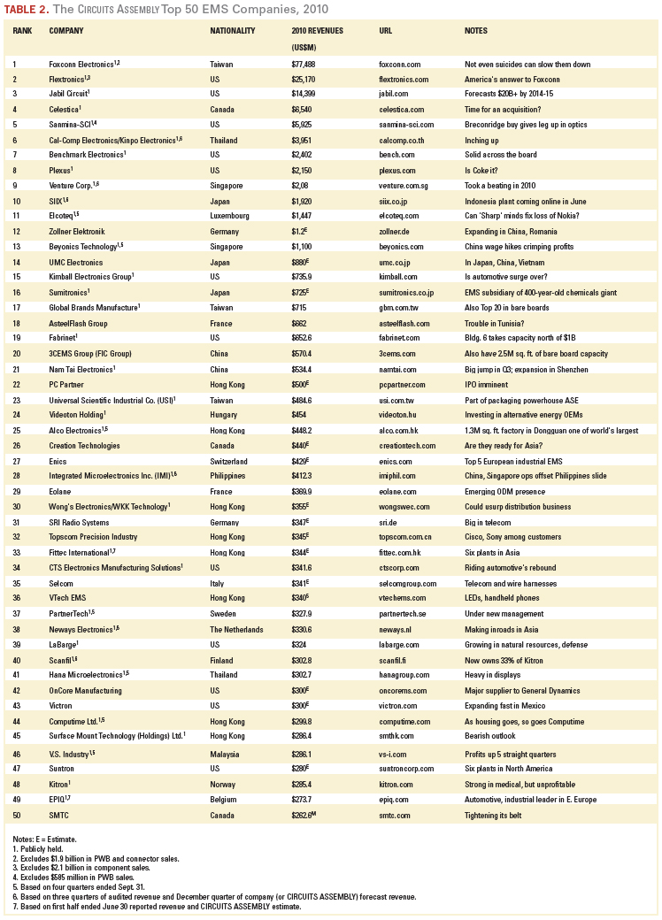
There was little change among the top 10 companies from 2009. Foxconn remains the clear-cut leader, well ahead of No. 2 Flextronics, which lost ground despite growing its EMS sales by $3.5 billion last year. No. 3 Jabil (up 23%) extended its lead over the rest of the pack, and management has plans to top $20 billion within four years. No. 5 Sanmina’s aforementioned acquisition of Breconridge helped it close the gap with No. 4 Celestica. Benchmark rose two spots to seventh and No. 10 Siix leveraged a huge year (up more than 35%) to displace Elcoteq, last year’s No. 7, from the Top 10. Venture, last year’s No. 8, slipped one spot.
The 2009 recession lowered the bar for entry into the Top 50. The cutoff for last year’s revised list was almost $200 million. 2010 changed that. For this year’s list, the cutoff was about $263 million, leaving worthy companies such as KeyTronic EMS out of the chart.
Still, the rising tide did not lift all regions, let alone all ships. While North American and Asia generally rebounded, the EMS industry in Europe continued to list. Kitron, Scandinavia’s third-largest EMS after Elcoteq (which is based in Luxembourg in name only) and PartnerTech, suffered through component shortages, plant closures and management changes. After eight straight quarters of losses, No. 11 Elcoteq turned profitable in the first quarter of 2010, and in the June period broke a streak of six consecutive quarters of falling revenue. Still, the third quarter saw lower sales and more losses, leaving the company-estimated sales down 30% for the year; the firm dropped out of the Top 10. On the other side of Eurasia, Hong Kong’s Alco’s revenue slid 33% from last year, and its ranking fell likewise (to No. 24 from No. 16).
By country, the US remains the home to the largest share of the biggest players (Table 3), with 12 entries, one less than in 2009. Hong Kong rose by two, to seven, the result of two omissions from last year’s Top 50. Canada lost an entry to an acquisition. The UK, once home to powers like MSL, was left without a single entry.
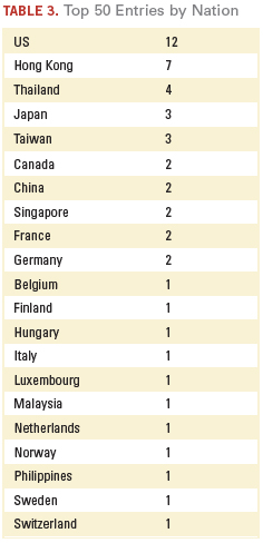
Of course, for many companies, the “home nation” is more a formality than a reality. For Foxconn, Flextronics, Beyonics, GBM, and several others, China is their largest footprint. Fabrinet is headquartered in San Francisco, but the vast majority of its factories are in Thailand. Given the violent uproars in the Middle East and much of Africa, it is safe to say there won’t be any new EMS facilities in those regions soon. As such, Table 3 will likely be very similar next year as well.
CIRCUITS ASSEMBLY is not the only entity that tracks the top EMS players. So why does our list occasionally disagree with those of other industry watchers? One reason is that we make our best effort to count only the revenues derived from EMS sales. Thus, companies like Foxconn, Flextronics, Hana Microelectronics, OSE, Sumitronics and Sanmina-SCI appear tens of millions and sometimes billions of dollars smaller than they truly are. Our belief is this gives a truer picture of the actual EMS sales, as opposed to revenue from connectors, bare boards, sensors or other unrelated components.
A few words about Foxconn. Although it is undisputedly the world’s largest ODM/EMS player, Foxconn is almost inscrutable. Most industry watchers know it is a major supplier to Dell, H-P, Sony and, of course, Apple, but plenty of smaller OEMs use its services too. Besides EMS, it is one of the world’s largest bare board fabricators – sales reportedly are somewhere between $700 million and $1 billion – and is among the top 10 in connectors too.1 It is quickly becoming a major supplier of LCD screens (which suggests Apple TV is not far off), and is headed toward a top 3 position in branded motherboards. Some rumors about the company are occasionally so off-the-charts outlandish, such as one making the rounds last fall suggesting Foxconn would invest $10 billion (not a typo) in a plant in Chengdu, China, that it’s a wonder how they get published.
But there’s the rub. Though public, Foxconn is traded on the Taiwan Stock Exchange, whose standards are relaxed relative to other major exchanges, and accordingly, the company-reported data are incredibly vague. What would seem its primary website, foxconn.com, hasn’t been updated in months. Its subsidiaries, such as cellphone ODM unit Foxconn International Holdings, sometimes have related names, but other times they don’t (witness Q-Run and Hongfujin Precision Industry Co.). And its subsidiaries have subsidiaries: Hongfujin reportedly is China’s largest exporter and has at least 60 other companies under it, which combine for roughly $30 billion in revenue.2 It has begun to open retail stores in China under the name Cybermart; it’s unclear how much revenue the 35 or so sites have generated thus far, but given Foxconn’s size, it’s unlikely to be material. Is Foxconn as large as the figures claim? It says here, no. But very few people can know for sure.
References
1. Ron Bishop, “The Top 10 Connector Companies,” ConnectorSupplier.com, August 2010.
2. Ling Ruiming, “Foxconn Faces Tough Competition from Rivals,” China Daily, Nov. 30, 2009.
Mike Buetow is editor in chief of Circuits Assembly; mbuetow@upmediagroup.com.
Ed.: Due to a currency translation error, Team Precision is incorrectly listed in the Top 50. Team Precision's actual calendar 2010 revenue was about $71.3 million. SMTC, at $262.6 million, should have been ranked 50th. Also, due to a spreadsheet miscalculation, VTech EMS' revenue was initially incorrectly calculated. We regret the errors.
In December, H2 Equity Partners announced a deal to acquire Assembléon (assembleon.com), putting to rest the lingering speculation over where the placement OEM would end up after longtime parent Philips put the company on the block.
H2 is buying a company that has rebounded strongly – revenue was up 90% in 2010 – from the last recession, and comes with its channel and equipment partners (namely, Yamaha) intact. CIRCUITS ASSEMBLY Editor in Chief Mike Buetow spoke this week with Assembléon CEO Andre Papoular about the pending deal and what it means for the company going forward.
CA: When will the deal close?
AP: We don’t know yet. We are working on many things and plan for the closing during the first quarter. The Dutch Works Council has to give its advice, and we need to get regulatory approvals.
CA: H2 Equity Partners has quite a variety of holdings, from staffing to potato breeding. What makes Assembléon a good fit?
AP: The size, shape and potential of the business are the characteristics H2 has looked at. They focus on midsized companies – we are on the high side of that – with headquarters in Germany, the Netherlands or the UK. They look at businesses that have gone through a certain cycle, have started to turn around and have a strong growth potential.
CA: In terms of size, how large is Assembléon relative to its other holdings?
AP: We are north of the bandwidth.
CA: How many years does H2 typically hold an investment?
AP: They present themselves as long-term investors and have kept many of their businesses for five to seven years. We are operating in a cyclical industry. The duration of the cycles and their impacts on the business performances, including growth opportunities, are influencing quite a bit of the time to invest and moment to divest.
CA: Has H2 given you any insight to any changes it has planned for the company?
AP: No. They looked at the strategy and footprint we have, the size of the organization, and our core competencies. They have no plans for major changes, as long as Assembléon delivers according to the plans. They will bring experience in accelerating turnarounds. They have knowledge of efficient supply-chain practices I hope we can benefit and learn from. They want to build on what we have started, as long as Assembléon delivers on its commitments.
CA: What metrics does H2 use for measuring success?
AP: General business performance ratios such as EBIT, cash, sales and market share development. It is difficult for them to set any targets yet. What is clear is that moving away from Philips to being owned by H2, we will really need to behave as a standalone company. We start with our own clean balance sheet and financing. This will give us some constraints on one side and allow us to take faster decisions and execution on the other.
CA: Has H2 asked for or planned any specific management changes?
AP: Not that I’m aware of. They have asked for continuation of the management team. We need to make sure the transition is seamless. For our suppliers, customers and people we are in business with, continuity is important. [H2] may decide on some changes later, but nothing is planned upfront. The business needs and performance will define the necessary changes and their timing.
CA: Will Assembléon make any changes to its regional offices or channel partners?
AP: There will be no change in footprint, no change in strategy, no change in management team. We are continuing with the support and expertise of H2 to help Assembléon accelerate its turnaround.
CA: What about the deal with Yamaha?
AP: It will not be impacted by the deal with H2. It has been known for many years by Yamaha that Philips was working on the divestment. We went for a neutral partner and with H2 – there is no competition between Yamaha and H2 – there is no reason for Yamaha to look at Assembléon in different ways. From our side, we clearly value the continuation of our partnership with Yamaha.
CA: Will H2 support the R&D work on the “A” lines?
AP: Yes. What I can say is we have within Philips an Annual Operational Plan. We have agreed with H2 that in case the transaction takes place, our current plan will be maintained as is.
CA: How have your revenues been year over year?
AP: They have increased 90% from 2009 to 2010.
CA: Several placement OEMs have been for sale for some time. Did the recent sale of Siemens help push this deal along?
AP: Not really. H2 has been looking at Assembléon for awhile. Our performance last year confirmed that we achieved what we committed to and created the right attractiveness and conditions for a deal.
CA: Why do you think placement equipment OEMs continue to find a home within the Japanese parent companies, while the European and North American-based placement OEMs are not seen as a good fit?
AP: I am convinced that the Japanese culture and values related to engineering, manufacturing and industry play a very strong part here. Japan has a strong base and history in industrial precision equipment. Look at how proud Yamaha is of being in this industry. They are extremely strong in vertical integration with all the necessary competencies that create good conditions for success. To compete efficiently, we need to apply a different business model, building on our core competencies and teaming up with the right partners to provide the rest. Next to this, we have to create an agile “end to end” value chain (from customers to raw material suppliers) that will act fast, sharing knowledge, innovation and capabilities to respond to dynamic market demands.
Last but not least, I don’t forget that we are moving away from a very well-known company, and I want to highlight that Philips has clearly started the process of identifying its core and no-core businesses years ago. Since then Philips lived up to its commitment of properly divesting its non-core businesses. Philips did everything it should to lead to the right moment and conditions for the divestment. Now it is up to Assembléon to write its next chapter.
Be sure your designs reflect the assembler’s soldering methods.
It’s getting very difficult to hand solder many parts these days. Some give it a try, but in general, if you’re dealing with the really tiny parts or leadless parts, it’s just not possible, or at least not practical.
Sometimes a designer will start with the idea of hand soldering the board, and then either decide against it when first looking at the raw PCB, or will build one and then decide it’s too much work. That’s not a bad thing. You can get more reliable assembly, and it keeps me employed. But there are times when a layout designed with hand assembly in mind does not work for machine assembly.
Case in point: Figure 1. There are two things wrong here. The first is that the land pattern is for a smaller part than the actual component. Let’s pretend that problem doesn’t exist. The other problem is that big via hole in the middle of the pad. When hand soldering parts with a solder pad underneath, like QFNs or QFPs, folks will often put a large hole there. They’ll solder the outside connections first, then turn the PCB over and stick a soldering iron and some solder in that big via to solder up the pad.

That works more or less for hand soldering, but it’s a really bad thing to have a big open via like that when machine-assembling parts. The solder will flow down and out the other side. You’ll get a mess on the bottom of the PCB, and you may get little or no solder on the pad.
The moral of this story is that if you’ve designed your PCB for hand soldering and later send it out for automated assembly, go through the layout and make sure you remove things put in there for hand soldering that aren’t conducive to reliable machine assembly. And, coming back to the incorrect footprint, make sure your CAD library land patterns match the actual part being used.
Duane Benson is marketing manager at Screaming Circuits (screamingcircuits.com); dbenson@screamingcircuits.com.
