


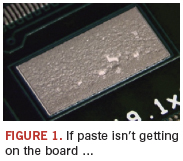
What to do when solder isn’t penetrating the aperture.
Insufficient fill occurs when the amount of solder paste deposited on a printed circuit board by the printer is much less than the stencil opening design.
Among the potential causes:
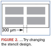
Stencil: Paste scooping effect, especially on large pads.
Recommendation: Segment the large opening into smaller apertures.
Screen printer: Paste does not roll into aperture.
Recommendations:
- Reduce print speed.
- Increase print pressure.
- Adopt lower squeegee contact print.
- Ensure paste is not expired or dry.
- Ensure sufficient board support.
- Reduce squeegee pressure.
Paul Lotosky is global director – customer technical support at Cookson Electronics (cooksonelectronics.com); plotosky@cooksonelectronics.com. His column appears monthly.

Consider the component and the coating process, not just the speed.
Coating contamination was found under UV light inspection. The coating process has caused the material to contaminate the surface of the connector pins. This assembly was coated with an automatic spray system that was probably incorrectly set up for production. The overspray (Figure 1) is visible under UV light on the surface of the gold connector pins and the body of the part. The contamination can also be seen on the black body of the connector.
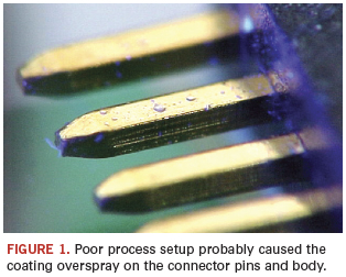
Some connectors are poorly designed for coating, permitting the fluid to capillary through the body/pin interface, leaving residues on the surface of the pins. Provided there is a gap between the connector and the coating line, a good, well-defined process should achieve contamination-free coating. A process engineer needs to look at the head type, coating material and the process parameters in detail, and not just focus on the speed of application. Slowing the process is still much faster than manually masking the connector with tape!
The connector pins can be reworked using a cleaning fluid recommended by the coating supplier. The cleaning material should not damage the board or the connector body. As gold contacts are inert, there should be no issue with contact resistance, but other plated connector termination surfaces may need to be tested. It’s important to run test boards or cards to check for correct setup and spray application, then inspect the sample prior to running the process. It is not time-consuming and can be conducted in less than 5 min.
These are typical defects shown in the National Physical Laboratory’s interactive assembly and soldering defects database. The database (http://defectsdatabase.npl.co.uk), available to all this publication’s readers, allows engineers to search and view countless defects and solutions, or to submit defects online.
Ed. Join Bob Willis and members of the NPL team for free process advice during the “NPL Defect Database Clinic Live” at IPC Apex.
Dr. Davide Di Maio is with the National Physical Laboratory Industry and Innovation division (npl.co.uk); defectsdatabase@npl.co.uk. His column appears monthly.
Component Assessment
“Compliance, Risk and Cost of Ownership Comparisons for Medical Device Sterile Products, Materials and Components Continuous Monitoring”
Author: Ken Appel; ken.appel@vaisala.com
Abstract: A guide to evaluating costs of monitoring critical environments while controlling risk factors. Six different modalities used in medical device and medical products’ materials and components industries for continuous monitoring – chart recorders, standalone data loggers, wired LAN networks with UPS backups, wired LAN networks using Power over Ethernet; WiFi; and Wireless Mesh – are systematically explained and compared in terms of costs of ownership and risks of non-compliance and loss in the context of today’s regulatory environment. (Company white paper, November 2010)
Environmental Management
“PVC-Based Composite Material Containing Recycled Non-Metallic Printed Circuit Board (PCB) Powders”
Authors: X.J. Wang, et al.
Abstract: A study of the use of non-metallic powders obtained from comminuted recycled paper-based PCBs as an additive to polyvinyl chloride substrate. The physical properties of the non-metallic PCB (NMPCB) powders were measured, and the morphological, mechanical and thermal properties of the NMPCB/PVC composite material were investigated. Results show that recycled NMPCB powders, when added below a threshold, tended to increase the tensile strength and bending strength of PVC. When 20 wt% NMPCB powders (relative to the substrate PVC) of an average diameter of 0.08 mm were added, the composite tensile strength and bending strength reached 22.6 MPa and 39.83 MPa, respectively, representing 107.2% and 123.1% improvement over pure PVC. The elongation at break of the composite material reached 151.94% of that of pure PVC, while the Vicat softening temperature of the composite material did not increase significantly compared to pure PVC. The results suggest that paper-based NMPCB powders, when used at appropriate amounts, can be effective for toughening PVC. (Journal of Environmental Management, December 2010)
Stencil Manufacture
“System for Laser Micromachining of Thin Metal Foils”
Author: Robert Barbuchaa, Marek Kocik and Jerzy Mizeraczyk; brobert@imp.gda.pl.
Abstract: A prototype of a laser system for micromachining of the materials (ULMM) is presented. This system is used for metal foils cutting, in particular for cutting stencils used in printing solder paste for PCB assembly. The system consists of prototype Nd:YAG laser; motorized deflection mirror; precise X-Y table with pneumatic metal foil holders; and control unit with custom software. A deflection mirror is used to obtain a trapezoidal shape of cutting edges, which is significant for PCB manufacturing. The X-Y table is based on modern planar motors, which have maximum velocity of 1 m/s at 20g acceleration. This system is capable of cutting holes with diameters of 10 µm and precise trepanation of the holes with diameters of 50 µm. (XVII International Symposium on Gas Flow, Chemical Lasers, and High-Power Lasers, April 2009)
Surface Finishes
“Effect of PCB Surface Finishes on Lead-Free Solder Joint Reliability”
Authors: Xu Zheng, Hongfeng Ran, Lei Wang, Hao Kou, Yexiang Ning, Bei Wang, Xian Lin, and Zuyao Liu
Abstract: The reliability of SnAg3.0Cu0.5 (SAC 305) solder joints with four kinds of PCB surface finishes was studied under isothermal aging at 125°C, including electroless nickel and immersion gold, organic solderability preservative, immersion silver and immersion tin. Their intermetallic compound composition and morphology were investigated by SEM/EDX, and the crystallographic features of IMC determined by XRD. Then the evolution of the microstructure of solder joints under isothermal aging was reviewed. Results showed the IMC grains on ImSn pad were unequal, with larger length/diameter ratio, and had different crystal orientations from that on OSP and ImAg pads. The high content of phosphorus in ENIG resulted in the emergence of phosphorus-rich and Ni3SnP multilayer after aging. Moreover, the mechanical properties of the solder joints with four PCB surface finishes were also studied via QFP pull test and high-speed solder ball shear test (HSSBS). Combined with the fracture analysis and mechanical test results of solder joints, it was found that the differences of failure modes and reliability performance were related to solder joint microstructure. ENIG pad showed poor reliability performance in HSSBS test due to the presence of phosphorus-rich/Ni3SnP multilayer structure after aging and interface micro-crack defect. Last, the electrical properties of different solder joints were evaluated by comparing their electrical resistivity. Owing to different composition and IMC crystal orientation, the resistivity of ImSn and ENIG pads after aging increased, while those of OSP and ImAg pads decreased. (Journal of Surface Mount Technology, October - December 2010, vol. 23, no. 4)
This column provides abstracts from recent industry conferences and company white papers. Our goal is to provide an added opportunity for readers to keep abreast of technology and business trends.
A look back at friends and colleagues who left us in 2010.
2010 was a year of recovery, but some unfortunately did not make it to see the industry complete yet another cycle. This month we reflect on their impact on our industry and our lives.
George Solorzano, 61, circuit designer and engineer at Southwestern Bell.
Chris Kimball, 63, sales executive, Virtex Assembly Services and president of Austin (TX) SMTA Chapter.
Park Ji-Yeon, 23, semiconductor engineer, Samsung Electronics.
Dieter Brammer, 70, longtime soldering expert for Vitronics, and founder of Screen Printing Technology and ABW Systems.
Wilbert Amos Moore, 81, aerospace electronics engineer.
Frank Racey, 70, sales manager, Peter Parts.
Dr. Carl Miller, 89, US Air Force radar genius who helped design the first successful launch of a live animal into space.
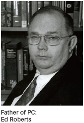
Dr. H. Edward Roberts, 68, father of the PC and mentor to Bill Gates.
Vincent D. Russell, 78, founder of PCB manufacturer R&D Circuits.
Jack Bradley, 57, sales representative, Bradley Representatives.
Dr. Fritz Sennheiser, 98, founder and longtime chairman of Sennheiser Electronic, a leading maker of high-end audio equipment.
Gordon Arbib, 67, former chief executive of Multicore Solders.
Rich Freiberger, 62, chief operations officer at ZF Array Technology and former vice president of technology development for GSS Array.
David Armstrong, 53, CEO and president, Armstrong International, owner of EMS firm Computrol.
Jack Robertson, 78, electronics industry journalist at Electronic News and EBN for some five decades.
Richard Vieser, 82, former Varian Medical chairman, and longtime director of Fisher Scientific, Control Data and Viasystems.
Dr. John Roy Whinnery, 92, retired director of the University of California-Berkeley Electronics Research Laboratory; innovator in electromagnetism and communication electronics; author of Fields and Waves in Communication Electronics.
Special consideration for the 14 employees who died on various Foxconn campuses this year.


North America’s “other” assembly trade show had reason for cheer.
The SMTA International trade show in late October was a good show. A good regional show – Orlando is not the center of the electronics assembly universe, after all – but a good one nonetheless. Traffic on the show floor was strong the first day, and not bad the second morning before slipping off to the usual end-of-show vacancy. (SMTA said attendance was up 20% over last year’s show in San Diego.) The technical sessions were very strong; the session on EMS that I chaired drew about 30 attendees, about as high as ever.
Tom Sharpe, vice president of component distributor SMT Corp. (smtcorp.com), gave a scintillating keynote on a trip to China, showing just how systemic counterfeiting operations have become. He notes some 29,000 incidents of counterfeits were reported to the US Department of Commerce between 2005 and 2008. And he warns that the process by which some are marking fake parts now renders the ink impermeable to scratches, which means simple tests for isolating counterfeits may no longer work.
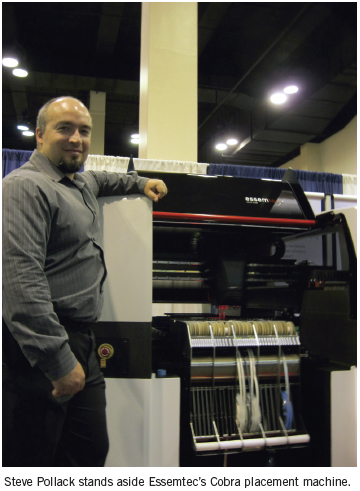
As is typical of regional shows, there was not much new in the way of technology. What did make the trip was worth seeing, though. DEK (dek.com) debuted its ProActiv squeegee, which oscillates during the print stroke in order to pack more paste into the apertures. My old friend Phil Zarrow points out that the concept isn’t exactly new – roughly 25 years old, perhaps – but sometimes good ideas take awhile to find their place. Essemtec (essemtec.com) is beta testing its Cobra system, scheduled for released in January. It features 220 inline intelligent feeders that can be changed (“hot swapped”) during production and 30 µm accuracy at 3 Sigma.
Aqueous Technologies (aqueoustech.com) debuted its Trident One Shot system, the lowest cost defluxer the company has ever manufactured. It offers fill-and-drain for low-volume applications, and uses a minimal 4 oz. of chemical every cycle. Mirtec, which sold an MV-3L desktop AOI system at the show, introduced its ISIS system with five 10-Mp top-down/side angle cameras.
Those who blanch at the thought of placing 01005s better sit down. Assembléon’s (assembleon.com) Greg Berry, global director, medium volume solutions, talked about the next-generation of chip packages: 005005 (or metric 0201). Half the size of an 01005, they should reach production within two years.
There was more than a little handwringing over the prices of tin and other metals, which at press time were skyrocketing. Some materials vendors intimated that China may be holding on to stocks, as it has cut its export quotes by 10% for 2011. On the product side, Cobar (cobar.com) president Stan Renals mentioned three new fluxes are coming, probably by March. FCT Assembly (fctassembly.com) has completed a study on paste shelf life that revealed certain products can last up to nine months and can be exposed to air for up to 24 hr. without degradation. President Tetsuro Nishimura proudly showed photos of Nihon Superior’s (nihonsuperior.co.jp) new R&D center in Osaka, Japan.
There were a few notes to share on the qualification side as well. Acculogic (acculogic.com) showed its ThermalScan product that features an IR camera to scan the board, conduct a thermal signature and show hot spots. SolTec Electronics (soltecelectronics.com) is putting decapsulation specialist Don Davis’ background in failure analysis to good use through a new non-destructive service to help EMS companies determine whether chips are counterfeit. DivSys (divsys.com), a new company run by former managers of Diversified Systems, discussed its third-party bare board qualification services.
Juki (jas-smt.com) president Bob Black said the leads were much better than last year. Juki is now back to its 2007 sales and production levels, he added. Dynatech’s (dynatechsmt.com) Mike Foster, who handles Samsung’s placement equipment in the US, added that machine backlogs reached 600 this year. Mirtec’s North America unit (mirtecusa.com) had its best October ever, and revenues are up about 70% over last year in Korea.
One last note: As he received the SMTA Founders Award, given to individuals for exceptional contributions to the industry and support of SMTA, Libra Industries (libraind.com) founder Rod Howell made an extraordinary gesture with a $5000 donation to the Charles Hutchins Grant. The grant underwrites the costs of a student doing post-graduate work in the fields of electronics packaging or assembly. And the SMTA has renamed its best paper award in honor of the late Rich Freiberger, a former director of the trade group and one of its most avid supporters. A nice touch.
Mike Buetow is editor-in-chief of CIRCUITS ASSEMBLY; mbuetow@upmediagroup.com.
Essential features of robust ESD control programs per ANSI/ESD S20.20.
What does best practice mean? It boils down to a quality system that results in the highest yield and the highest quality product. In the case of ESD control, it not only means high yields, but also no hard or latent defects in parts shipped to customers.
An excellent place to start for protecting ESD-sensitive devices is to implement an ANSI/ESD S20.20 static control program. ANSI/ESD S20.20 (hereafter called S20.20) requires two main areas be specified: administrative requirements and technical requirements. A careful review of S20.20 reveals some overlap in the requirements; however, they support each other well. Administrative requirements define the program and many of its necessary “non-technical” elements (the first four items below); the rest is documentation of the technical requirements that make up the program.
The administrative requirements in S20.20 define an ESD control “plan.” The plan must document several items:
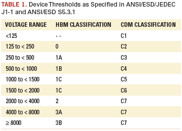
Device sensitivity determination. A first step is to understand how sensitive your products are to electrostatic discharges. It is important to have some idea of both Human Body Model (HBM) and Charged Device Model (CDM) sensitivities because, in most cases, these will be very different. While knowing the exact withstand voltage of every device is not necessary, know the general sensitivity of the parts handled. For instance, if manufacturing boards with standard CMOS-like components, the typical HBM withstand voltage will usually be in the 1000s of volts range, and the CDM values will usually be 500 - 1500V. This ESD control program would look very different than one in the hard disk drive industry, for example, where handling of parts with reportedly less than 1V CDM ESD thresholds is becoming common. The current HBM and CDM test methods loosely classify device sensitivities (Table 1).
Industry has recognized all devices have become more sensitive over the past 20 years, yet the classifications haven’t changed. Most ESD practitioners realize many of the most sensitive parts fit in a subset of the most sensitive classifications (HBM Class 0 and CDM Class C1). It is especially important to know if you have any of these devices. As far back as the mid 1980s, AT&T researchers realized they were manufacturing and handling parts well below the lower threshold of the most sensitive ESD classifications used at that time and adopted the phrase “Class 0,” which referred mostly to CDM values (even though CDM was a barely-heard-of ESD failure mechanism at the time). They did this to highlight that these devices needed extraordinary protection beyond the standard ESD control programs at the time. More recently, “Class 0” has been used in various areas of the industry. While some ESD control practitioners have objected to the use of the term, most who do use it realize it simply means “a very sensitive device.” While further discussion of the “Class 0” classification is beyond the scope of this article, suffice it to say that if you believe you are handling what the industry has been calling “Class 0” ESDS parts, at a minimum, develop a robust ESD control program or expect yield and reliability issues.
Assignment of an ESD program manager/coordinator. The organization must document the appointment of a coordinator or manager of the ESD control program. The purpose of this is to require management to take the ESD control program seriously enough to assign a person to this role. This is similar to the ISO 9001 requirement to assign a quality manager responsible for maintaining the quality system of an organization. The ESD coordinator is the focal point for the management of the ESD control program. This person is not required to have a certain level of training or certification; however, additional training in the technical details of ESD and ESD program management would be beneficial.
Training plan. The organization must have, and properly document, an ESD training program. The method of training, frequency of recurrent training and location of training records must be documented. In addition, a method of measuring the employee’s comprehension of the training material must be documented. This “test” can be a written test, on the job observation or another measurable method. The results of each test must be recorded and stored along with the training records. The training plan portion of S20.20 is the most common cause of formal assessment failures during an S20.20 assessment.
Compliance verification program. There also must be a documented compliance verification program for the organization. It is recognized that ESD control items and procedures lose their effectiveness if not continuously maintained. A defined and implemented compliance verification program ensures the ESD control program elements stay working during the life of the program. Some companies have chosen to have the compliance verification done by their own employees, while others have chosen outside vendors (such as a calibration test company). In any case, the more complicated the ESD control program, the more attention that needs to be paid to compliance verification.
For instance, a well-known disk drive manufacturer has four levels of compliance verification. The first lines of defense are the manufacturing operators. They are trained to do a visual check of their ESD controls at the beginning of each shift. They check not only their own wrist strap, footwear and garment systems, but they also do a visual check of their workstation, looking for ground wires, ionization discrepancies and non-ESD approved materials. The second level of compliance verification is a department technician that does a daily, weekly or monthly check of all ESD controls. An AQL-type of audit (statistical sampling) may be done on a frequent basis. However, enough items are inspected on a regular basis so that in a specified time frame all the items are checked. The third level is an audit performed by the ESD coordinator, ensuring inspections by the department technician are completed, and then spot-checking the ESD controls in each area. The fourth and final level is done by a third-party auditor on an annual basis. The compliance verification methods must be technically equivalent to those documented in ESD TR53, and the equipment used for the testing must be documented properly.
It is important to note that the most successful compliance verification programs are those that are regularly reviewed by management through reports that are made available to them, with subsequent follow-up to close corrective actions.
Grounding system. The system used to ground all conductive elements must also be defined. S20.20 describes three grounding systems: equipment (AC) ground, auxiliary ground or equipotential bonding system. One or more of these systems must be defined as the grounding system in the plan. This is followed by implementation of the grounding system defined. Many companies use more than one of the grounding systems. For instance, they may define the equipment (AC) ground as the primary method, but they may also define areas that use equipotential bonding for areas where the equipment ground is not available.
The second issue that must be documented as well is how personnel are to be grounded. Most companies simply state that all personnel wear a grounding wrist strap whenever working on ESDS items. Some allow the use of footwear/flooring if operators are standing. S20.20 requires seated operators to always be wearing a grounding wrist strap; any deviation requires a tailoring statement. (See below for “tailoring.”)
Documentation of the EPA (Electrostatic Protected Area) elements. This can be the largest section of the plan, as it defines the balance of the technical elements of the ESD control program. However, it can also simply refer to the S20.20 elements. Not all elements specified in S20.20 are required elements. However, if an element is documented in the plan, it then becomes an auditable requirement by an S20.20 assessor. An example of this is the use of garments. Many companies like to use garments in their factory for a variety of reasons. However, many don’t want to do compliance verification of the garments. If garments are formally documented in the ESD control plan, then compliance verification must be performed. An option is to require the use of garments somewhere besides the plan, which would avoid audit.
Another element typically addressed here is the flooring/footwear system. Table 3 in S20.20 specifies that the total resistance of an operator must be below 35MΩ whenever they are not using a wrist strap system. If the resistance is above 35MΩ, more testing must be done to verify that they do not generate more than 100V when walking. This is one of the most misunderstood sections of S20.20.
Packaging. The organization must specify packaging requirements for parts moving or stored inside and outside of the EPA. The safest way to do this is to specify packaging that meets the requirement in ANSI/ESD S541. It is important to address packaging in the compliance verification program as well.
Marking. Marking is another one of the misunderstood sections of S20.20. It is included mostly due to demands by the military that it be addressed. “Marking” includes both the signage used to identify the EPA, but it also is applied to the marking of packaging and actual devices that are ESD sensitive. Many commercial companies either make a simple statement that they mark packages containing ESDS components with a commercially available mark, or they state that no marking is required.
Tailoring. One of the strengths of S20.20 is the ability of the user to tailor the specification if necessary. Tailoring is not necessary if you choose to make requirements more stringent than those specified in S20.20. However, if you want to make a required element optional, or make a specified value less stringent, tailoring is required. For instance, to specify a lower resistance limit for work surfaces, no tailoring is necessary. However, allowing operators to not wear wrist straps when seated, or allowing work surfaces with a higher resistance-to-ground than 1 x 10⁹Ω, requires a tailoring statement. The tailoring statement must have technical justification and data to support the assertion that using the specification as-is is not necessary or deleterious to the product.
Additional thoughts. Products that fall into that “supersensitive” range may require efforts beyond the standard S20.20 program. For instance, for devices sensitive to charged device model damage, you may need to specify a minimum surface resistance value for work surfaces or anywhere else ESDS parts may touch, or you may need to limit metal-to-metal contact (say from tweezers or other tools).
You also may need to determine if more critical ionization is necessary to remove charge from product before it is handled or touched. Some companies are finding they must beef up the compliance verification program with more frequent or stringent testing. You also might benefit from beefing up training, highlighting critical items needed for the most sensitive products. Many companies dealing with ultrasensitive devices find that standard measurement tools are not enough. These companies find necessary the use of more robust process assessment tools, such as an electrostatic voltmeter and ESD event detectors. Some are using constant monitors for wrist strap, grounding and ionization verification to ensure these elements work continuously. Some companies have even implemented computer-based factory monitoring of these elements.
The “best” ESD control program is one that prevents any ESD damage to the components manufactured or handled, without overkill, resulting in expensive controls that may not be necessary. Certainly, an excellent place to start is to have a well documented and implemented S20.20 ESD control program. Additional controls may be necessary, depending on the sensitivity of the components handled and the manufacturing process complexity.
Ed.: For more on ESD programs, contact the ESD Association (esda.org).
Carl Newberg is president of MicroStat Laboratories (microstatlabs.com) and director of S20.20 Manufacturing Programs for Dangelmayer Associates, LLC; carl@microstatlabs.com.

Press Releases
- Zollner Puts a New Mechanics Building into Operation
- Changes in Incap’s Management Team: Incap updates its leadership model to support its growth strategy
- Niche Electronics Celebrates Completion of Florida Expansion
- Microscreen Names Nik Thomas Director, Expands Leadership Role Amid Continued Organizational Growth