

Identify and solve placement and reflow-related solder defects.
We continue our series on solder bridging. This month, we look at potential problems caused by the placement machine and reflow profile.
If the pick-and-place machine is suspected:
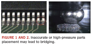
Problem: Placement inaccuracy narrows gap between pads, increasing the chance of bridging.
Recommendations:
- Verify component placement pressure.
- Use x-ray to verify BGA placement.
- Use microscope for QFPs.
Problem: Excessive component placement pressure will squeeze paste out of pads.
Recommendations:
- Verify actual component height against data entered in the machine.
- Component placement height should be ±1/3 of paste height.
If the reflow profile is suspected:
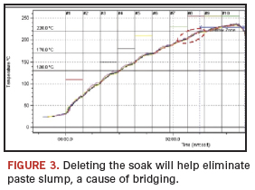
Problem: Extended soak will input more heat to the paste and result in paste hot slump phenomenon.
Recommendation: Adopt a straight ramp to spike profile, without soak zone if possible.
Paul Lotosky is global director - customer technical support at Cookson Electronics
(cooksonelectronics.com); plotosky@cooksonelectronics.com. His column appears monthly.

Eight steps to getting the best possible test coverage.
IEEE 1149.1 for boundary scan adoption has seen a steady climb in use for the past five years. In particular, it has gained popularity with NPI test engineers working with high node count printed circuit boards for telecom network servers/switches and PC servers. There are several ways to implement boundary scan test on PCBs, the two most common being:
- Native boundary scan on in-circuit test systems. (Note: Native boundary on ICT is an integrated solution where the boundary scan test will be developed and executed within the same ICT interface. No additional third-party hardware or software is needed.)
- Standalone benchtop boundary scan. Standalone benchtop boundary scan is preferred during prototype/NPI, as it enables PCB testing without building an ICT fixture. However, it has not been adopted for high-volume manufacturing, where the majority of manufacturers use the native boundary scan on ICT. Here’s why:
- Cost. A basic benchtop boundary scan setup is about $10,000 to $20,000. Additional licenses for development, debug and runtime features will increase the cost of the benchtop boundary scan solution up to two to three times the basic cost. Compared to the cost of using native boundary scan on ICT solution, the latter is practically free, as most EMS providers and ODMs would already have boundary scan licenses enabled on their existing ICT systems, which include development and debug features.
- Separate station. Running an extra station after ICT doesn’t appeal to most assemblers, as it means extra system and manpower costs, not to mention an additional process.
There are other minor reasons, such as local support, especially for the majority of high-volume manufacturing sites in Asia. Availability of expert support from the benchtop boundary scan vendors in Asia has not come far compared with that offered by ICT vendors. This is understandable, since ICT has been around for more than 30 years in electronics manufacturing, fostering a more robust support model.
These are just a few reasons why most assemblers prefer ICT for boundary scan test for volume products. Besides, ICT offers coverage for most of the PCB defect spectrum (opens, shorts), analog components value measurements, as well as powered test, which includes voltage measurements, clock measurements, digital test and in-system programming capabilities. Table 1 compares boundary scan test coverage of a typical benchtop boundary scan setup with an ICT offering boundary native scan capabilities. 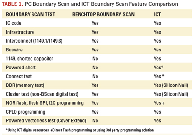
Although native boundary scan on ICT is the preferred solution during volume manufacturing testing, avoidable implementation issues can affect stability of the test.
Boundary scan tests, like any other digital test during ICT testing, are susceptible to noise, which affects stability. As such, the following best practices should be considered:
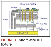
1. Assign critical attributes to JTAG pins (TDO, TDI, TMS, TCK and TRST) to ensure the shortest wire possible (Figure 1). To ensure signal quality and fidelity, consider assigning critical attributes to the JTAG pins during test development to ensure the fixture has the shortest wire possible (as short as 1") from the ICT system’s digital card pins to the test probe. The shorter the wire on those JTAG pins, the less the possibility of an adjacent wire crosstalk.
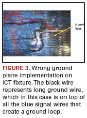
2. Proper fixture ground plane implementation. The main objective of using a ground plane on the ICT fixture is to reduce ground loop created by the distance between the ICT system ground and the PCB ground via fixture wiring. Unfortunately, few understand proper ground plane implementation, which can make or break the ICT digital or boundary scan test (Figure 2). The objective of having a proper ground plane is to help ensure the PCB ground is as short as possible to the ICT system’s digital ground during digital test, to minimize ground loop, as well as ensure that the signal wire stays closer to the ground to minimize crosstalk. Figure 3 is an example of a badly implemented ICT fixture ground plane, which is worse than not having a ground plane. 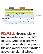
3. Twisted-pair wiring on JTAG pins (TDO, TDI, TMS, TCK and TRST). Aside from short wiring, another strategy to ensure signal integrity and minimizing noise is implementing twisted-pair wiring on JTAG pins. Twisted-pair impedance of approximately 100 Ω matches the low output impedance of the digital driver of the ICT system, which will result in a better drive signal integrity.
4. Removing physical test probes. For nodes that have only boundary scan devices connected to them (100% boundary scan nodes), removing these probes could ensure the signal integrity on those nodes stays clean. However, use a conservative approach in removing test probes on boundary scan nodes, as it will mean losing test coverage if there are non-boundary scan devices or analog components connected to it.
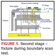
5. Dual-stage fixture. Most of the designs of high node count assemblies have resorted to a dual-stage fixturing solution where during the first stage, all the test probes are in contact while executing unpowered and powered in ICT (Figure 4). At the second stage, executed after all first stage tests have been passed, the fixture probe plate will move up either mechanically or via a pneumatic cylinder to disengage most of the normal test probes, with only a few long travel test probes remaining in contact. The test probes in contact during this second stage are power, ground, JTAG pins (TDI, TDO, TCK, TMS and TRST), as well as compliance and disabling pins (Figure 5). With the dual-stage fixture strategy, most noise coupled through the fixture wires is eliminated, resulting in a stable boundary scan test.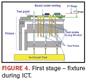
6. Power cycling or reset sequence. Adding a power cycling or reset sequence procedure to the test plan ensures the boundary scan devices in chains are in the proper state for testing. During boundary scan, the core logic of the devices in the chain is disconnected from the rest of the board, which probably would affect other devices operating in normal mode. Other devices exchanging data with boundary scan devices will consider the devices inoperable.
Note that when the board comes out of boundary scan mode, all the boundary scan devices go into BYPASS, and the core logic is reconnected to the I/O pins, but the board and the boundary scan devices do not necessarily pick up where they left off. To get the board back to normal operating mode, the board reset procedure must be run, or board power must be cycled. This can be done by adding a reset sequence or power cycling procedure to the test plan.
For multiple chains, interactions between chains can be a problem. For problems with connect tests or disabling difficulties, try adding a power cycling or reset sequence to the test.
7. Disabling upstream device, oscillator, switching voltage regulator. When a digital or boundary scan device is being tested, its surrounding devices can affect the way the device operates. This, in turn, can affect the test for that device, resulting in an unstable boundary scan test. To some extent, the effect that other devices have on the inputs to the device under test is minimized in the test system by overdriving. However, this is not always completely effective and cannot be used with high-speed signals. Disabling the upstream devices ensures that there is no other signal interference while executing boundary scan test. Disabling on-board oscillator and switching voltage regulators ensure that noise coupled through fixture wiring is minimized, which will result in a stable boundary scan test.
8. Maintaining JTAG pins signal during boundary scan test and disable state. Most PCBA with good boundary scan design for test implementation will take care of the pull-up/down resistor of the JTAG pins to ensure stability of the boundary scan test. If these DfT factors have not been included on the board, implementing them on the fixture will help.
The TCK (test clock) should be treated like any clock pin, although it has nothing to do with the on-board clock function. The TCK should be terminated with a 68 Ω resistor in series with a 100 pF capacitor to ground.
Maintaining stable TMS (test mode select) signals, either during boundary scan test or the disable state, is very important. During boundary scan test, the test generated by ICT will ensure that TMS will maintain its level according to the state diagram. However, during boundary scan test, disabled TMS should maintain a signal level to remain in the reset state. A pull-up resistor will help to ensure that TMS remains high.
TRST (test rest) is an optional JTAG pin designed to let the boundary scan test get into the TEST-LOGIC-RESET mode regardless of the state of TMS or TCK. Whenever TRST gets asserted alternatively in the absence of TRST pins, boundary scan will enter the TEST-LOGIC-RESET mode when TMS is held high for at least five rising edges of TCK. The TRST signal should include a pull-down resistor when possible to reduce the chance the signal floats when it is not being driven by the ICT driver.
The success of boundary scan test implementation on ICT lies not only with the tools used, but also the project team’s support of the strategy from design and test engineering up to production. With a new set of boundary scan-related IEEE standards (P1687, P1581, 1149.7, 1149.8.1) expected soon, boundary scan will get a further boost in the board testing environment.
Bibliography
1. IEEE, 1149.1-2001, “Standard Test Access Port and Boundary-Scan Architecture.” June 2001.
2. SMTA, SMTA/TMAG Testability Guidelines TP-101D, 2008.
3. Kenneth P. Parker, Boundary Scan Handbook, 3d edition, 2003.
Jun Balangue is technical marketing engineer at Agilent Technologies (agilent.com); jun_balangue@agilent.com.
Using preforms, balls can be removed and reattached in an hour.
Removing and reworking the BGA is often an economically attractive alternative to replacement with a new part. If the intent is to reuse the BGA, the solder balls must be replaced before it can be resoldered to the circuit board. The BGA removal process renders existing solder balls unusable.
Starting with a BGA removed from the board, the first step is to bake the moisture out of the component to prevent a defect known as popcorning. This defect appears as craters in the BGA package, caused by the explosive expansion of absorbed water vapor during reflow. It is easy to see on the top and sides of components, but after the solder balls have been reflowed, it can be more difficult to see on the underside of the component.
Next, remove the existing solder balls and clean the surface. Solder balls can be removed using a soldering iron with a blade tip attached. Uniform heating of the part with auxiliary heating is necessary to avoid localized thermal shock to the BGA from the hot blade. This method is adequate for bulk solder removal. Care must be taken not to scratch the BGA surface. Generous use of flux increases the effectiveness of the heat transfer and also removes any oxides. Solder braid is used next to remove smaller flecks of solder, also with generous flux.
As a final cleaning and preparation, the BGA is carefully washed with isopropyl alcohol (IPA) to remove flux. The part is then inspected. Cleanliness can be confirmed using standard resistivity of solvent extract (ROSE) or SEC (solvent extract conductivity) testing.
Specify the BGA type and part number to BGA reballing vendors in order to obtain the correct preform parts.
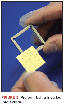
Continuing with a clean, solder-free BGA, the next step is to perfectly position the balls under the BGA. With hundreds of solder balls to be exactly positioned, a mechanical device is required to maintain the alignment and position the solder balls under the chip. The two most popular methods to actually attach the solder balls are the “preform” method and the “specialized fixture” method. The preform method holds solder balls in the exact pattern using a water-soluble paper carrier (Figure 1). This precise paper form is the key to this process and ensures the balls are aligned on the carrier within 0.0004".
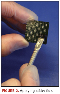
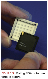
The perimeter of the preform is precision-cut to perfectly match the BGA dimensions. Mating the preform to the BGA is accomplished by applying paste flux to the BGA (Figure 2). The paste flux is sticky, and holds the BGA to the preform. A fixture is often used to speed assembly and ensure accuracy (Figure 3).
The next step is to reflow the two mating parts using a profile based on whether the solder balls are SnPb or Pb-free. The BGA assembly is processed through the reflow oven the same way a board is processed. The solder balls are now attached to the BGA.
Then remove the paper carrier (which is designed for easy removal). After part inspection, the BGA is ready to be attached to the board.
With some experience, good equipment and a mature process, the entire rework and BGA reballing process can be accomplished within an hour.
ACI Technologies Inc. (aciusa.org) is the National Center of Excellence in Electronics Manufacturing, specializing in manufacturing services, IPC standards and manufacturing training, failure analysis and other analytical services. This column appears monthly.

The wider the diameter, the faster solder joints will form.
Selective soldering generally uses two basic nozzle design types: One is the “round” nozzle, also known as a “bullet” or universal nozzle. It can approach any solder site from any direction, since it is completely radial in its design on the top.
The other is a component-specific wave or “letter-slot” nozzle, and its design is better suited to soldering rows of pins, such as found on an array. This nozzle shape is ideal for connectors, for example, a five or a six-row connector, with perhaps 40 to 50 pins in a row. One could use a round nozzle for such a job, but that would lead to a deviation in the overall soak time in the solder, because as the nozzle travels along parallel rows of pins, the pins in the center of travel dwell in the solder for the full diameter of the nozzle, but the pins on the outer edges – the outside rows – would see only a section of the diameter, basically an arc. As such, the dwell time under solder for the pins in the center actually could be twice as long as the exposure for the pins in the side rows. This can result in a variation in quality for the solder joints in the outside rows.
That’s when we prefer to use the wave nozzle, because it is designed for the component shape we are soldering; in this case, all the rows would see the exact same dwell time, thus ensuring consistency in solder joint formation quality.
In selective soldering, it’s important to get enough heat into the solder site, as rapidly as possible, to overcome the heat sink characteristics of the board and get good wetting and filling of barrels right up to the top side of the board. Accommodate longer pins, if encountered. To do this requires flexibility in the amount of “freeboard” of molten solder – the parabolic bubble of moving solder – at the top of the nozzle. Different suppliers use different methods of achieving this, from controlling pump speed to various nozzle design factors. What we find effective is a machined radial groove near the top of the inside of the nozzle that provides universal back pressure at the periphery, so that the solder in the center of the nozzle will rise higher than it would normally if the flow of the solder column were uniform.
The concept is simple, but the effect is to provide the greater freeboard of the parabolic dome of molten solder emerging from the top of the bullet nozzle. It also permits a high rate of solder exchange; this in turn provides a high rate of heat exchange, thermal transfer to the solder site, permitting proper hole filling in the barrel, a feat often difficult with multilayer, high heat sink boards. A higher freeboard actually lets the machine “pump” solder into the holes that need complete filling; but at the same time, we want a constantly controlled solder wave or fountain shape.
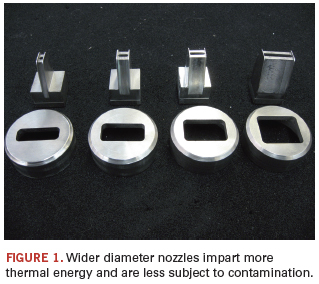
A rule of thumb in nozzle selection is to always use the largest diameter nozzle available that will handle every selective soldering task on the board; don’t skimp by using a small nozzle. If a bigger one can be used, all the better; the bigger the nozzle, the more thermal energy will be imparted to the board, and also the quicker the solder joints will form, thus reducing dwell time. Try to use the same nozzle for every site on the same board, if possible.
Practically all selective soldering equipment manufacturers provide wetted nozzles, and these deliver excellent performance. With these nozzles, the outside diameter of the nozzle is actually wetted by the solder. Everyone has their own particular approach; in our case, a proprietary alloy lets us achieve this wetted effect. Wetted nozzles provide more uniformity and control of the flow of the molten solder as it travels back toward the pot.
In many cases, for expediency, uniquely shaped nozzles can be designed to solder a number of sites and multiple solder joints simultaneously, in a stamping or a branding type of operation. For example, there might be multiple nozzles of various shapes in the same nozzle manifold that come up and stamp a certain pattern time and again. They might be a mix of square, rectangular, round and half-round, etc.
When Pb-free selective soldering, remember that even stainless steel nozzles are scavenged by the tin in the solder. SnPb alloys seem to have little effect on the longevity of stainless steel nozzles, but Pb-free alloys, and particularly SAC types, will erode the nozzle material, even stainless. One remedy is to coat the inside of the nozzles with a resistant coating to prevent or at least slow that erosion process. Erosion of stainless will add nickel content to the solder pot, and any type of dissolved metals contamination can impact solder joint reliability.
Have uniform control of the “freeboard” of solder above the nozzles. However, selective soldering nozzles, particularly smaller-diameter nozzles, are notorious for gradually losing the height of the solder freeboard over time due to the buildup of contamination inside the nozzle. Real-time measurement of the solder height that will automatically adjust pump speed in order to maintain a pre-set desired height is valuable here. That’s a critical part of the process. If solder height diminishes and you aren’t aware of it, soon you’re not soldering at all, or at least not getting the desired quality.
Selection, shape, design and function of selective soldering nozzles are a critical focal point of successful soldering. Know your nozzles! Understand their features, how they affect and control the solder wave, and what their vulnerabilities may be to the specific alloy used.
Alan Cable is president of A.C.E. Production Technologies (ace-protech.com); acable@ace-protech.com.

The company’s handling of a suicide cluster overshadows the context.
Foxconn Technology Group opened its first electronics assembly manufacturing plant in Shenzhen, China, in 1988. Today, that is the company’s largest plant, with 460,000 employees, about 16% of whom live on campus.
Founded in 1974 as a manufacturer of plastic products (notably connectors) by Terry Gou, who remains its CEO and largest shareholder, Foxconn has become the largest contract manufacturing company. But recently, the company has come under public scrutiny due to allegations of employee mistreatment. To date, 12 employees have jumped from company buildings in suicide attempts during 2010; only two survived (in critical condition). Likewise, the company’s critics have leaped to the conclusion that Foxconn mistreats its workers, but the situation demands greater nuance and understanding. This cluster should be investigated, and indeed the government and Foxconn’s customers are doing so. Managers have provided trained counselors in a care center since April and a suicide hotline since last year, which has been expanded significantly amid these tragic events. 
The issue has been exacerbated by Gou’s lack of understanding as to why the suicides are happening. Guo recently commented that it is not possible to determine any one cause for these tragic suicides and seems mystified as to why an employee would take their life. The company responds that Gou has been based in Shenzhen since May, leading a team addressing these very complex issues.
The deaths are thought to be related to working conditions at the plant: long hours for poor pay and constant pressure to perform. Indeed, the company’s operations and demanding working conditions (although not nearly as bad as the conditions in China’s coal mines) appear cause for despair. Workers complain about military-style drills, verbal abuse by superiors and “self-criticisms.” They reportedly are forced to read aloud, fined for unwritten abuses (talking to coworkers, tardiness, etc.), as well as allegedly pressured to work as many 13 consecutive days to complete a big customer order - even when it means sleeping on the factory floor.
Foxconn denies these allegations, and claims to follow EICC overtime guidelines of a maximum of 60 hours per month. (The company also says it will abide by China’s pending overtime guidelines of no more than 36 hours per month.) Moreover, the company’s recent wage hikes purportedly ensure that workers will not have reduced wages with reduced overtime hours.
It’s true that Foxconn has done itself no favors. A young manager killed himself last July after an Apple iPhone prototype went missing, and his final messages to friends suggest he had been interrogated and beaten. In a separate incident the following month, the company confirmed its guards beat employees after a video surfaced of the episode. In 2006, after a Chinese newspaper reported that employees were being abused, a charge later shown to be false, Foxconn sued the two reporters personally and sought to have their assets frozen, provoking a public backlash against the company.
Gou’s own lack of awareness has not helped the situation either, although he has made repeated efforts to apologize to the families of the deceased. However, in a recent shareholder meeting Gou announced, “If a worker in Taiwan commits suicide because of emotional problems, his employer won’t be held responsible.…” Such statements seem aimed at keeping the company financially strong rather than honestly facing the core problem.
Suicide results from depression and the belief that there are no other options. Indeed, when a worker comes from the country to work and send back money to their family, and this does not happen, it can be basis for despair. One inside reporter confirmed this by saying that young people frequently come to Foxconn hoping to eventually start their own business or go to college, but most never realize that dream. According to the New York Times, recent interviews with employees said the typical Foxconn hire lasts just a few months before leaving, demoralized.
Sociologists and other academics see the deaths as extreme signals of a more pervasive trend: a generation of workers rejecting the regimented hardships their predecessors endured as the cheap labor army behind China’s economic miracle. While the EMS industry drives productivity to the extreme, and at times can be extremely demanding and punitive, it is not necessarily the cause of despair and hopelessness that sometimes causes people to commit suicide, although it can be a contributing factor.
Regardless, the company could do more to alleviate the conditions for despair and demoralization. For example, on May 27, 2010, the Shenzhen Post related the case of a typical Chinese female worker named Happy, a 19-year-old assembly line worker. She sends back home as much of her 1000 RMB ($150) monthly salary as possible, but with Foxconn’s severe penalties for unwanted kinds of behavior, this dream seems remote. For example, Happy likes washing her own clothes by hand; she claims it calms her in times of stress. Her factory mandates uniforms be dry cleaned, however; if she washes it, she is penalized 500 RMB. If she is late, she is charged 100 RMB per minute. If she refuses or can’t work overtime when needed, she is removed from work lineup for over a month, or until she can come up with the fee for reinstatement. Talking during working hours brings a 100 RMB fine. She even had to borrow money once to pay the negative balance from her salary. Such conditions would leave anyone feeling hopeless.
Subsequently, the rash of suicides has intensified scrutiny of the working and living conditions at Foxconn. Responding to the clamor, Foxconn has offered to double salaries in three months’ time, setting a new standard for many other local companies such as Honda. Moreover, the company is building an enormous safety net in a pathetic effort to stop people jumping to their deaths, but a recent attempted suicide by a young man who slashed his wrists shows that such efforts will not deter those determined to take their own lives.
The gap in recognition of the problem underlying why a person commits suicide was further reflected in Gou’s proposed solution to get all employees to sign a non-suicide pact. Employees have already complained that the letter makes it seem like they could be carted off to a mental hospital if they argue with a supervisor, and that they don’t know what the consequences are if they don’t sign. The company has since been forced to withdraw the letter. In a seemingly final act of desperation, in May 2010, DigiTimes reported that Guo sought the aid of an exorcist to try to put an end to the tragedies. (Foxconn representatives noted this is a common cultural practice in China when a death has occurred.)
Overall, indications are that conditions in Foxconn’s factories are good and job applicants are eager to work there. By in large, most workers are happy to submit to the culture and receive overtime opportunities. Yet, the labor intensity is high and Chinese workers have commented that many Westerners would find it difficult to work at Foxconn. As BBC News recently quoted one employee, “I always smile when I see pictures of Chinese workers asleep at production lines; this is their culture. Chinese are taught from school that lunch time is nap time. The 1.5-hour lunch break is common practice, almost sacred. How often do we have that in the West?”
The problem of ongoing suicides at Foxconn needs to be put in perspective. Twelve people (at last count) seems a lot, but the firm has an estimated 800,000 workers, more than 460,000 of them at a single campus in Shenzhen. According to the World Health Organization, China’s suicide rate is 13 males and 14.8 females per 100,000 people (by comparison, the US has 11 per 100,000). In other words, Foxconn’s suicide epidemic is actually lower than the national average in China and many other countries. Unfortunately, this says nothing about the fact Foxconn is the only EMS company in Asia that seems to be experiencing this problem.
Suicide is too complex an issue to rush to conclusions, and the working conditions in China are improving. For the time being Foxconn seems to be taking its responsibility to its workers’ health seriously and deserves the benefit of the doubt.
Randall Sherman is president and CEO of New Venture Research Corp. (newventureresearch.com); rsherman@newventureresearch.com. His column runs bimonthly.
A study of 40 leaded and Pb-free solders compares alkaline to newer cleaning technologies.
PH-neutral product technologies that are fully compatible with anodized aluminum parts, sensitive metals and other challenging substrates are now available. Despite the absence of alkalinity, pH-neutral chemistries can still complete the job of defluxing agents. Their unique physical properties also come into play as users strive for minimal equipment wear-and-tear, which had not been the case in the past. Equipment replacements are costly and can add significantly to the overall process cost. Safety is also improved if operators can completely avoid working with caustic materials.
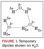
The performance of today’s pH-neutral, aqueous cleaning agents hinges on previously unknown reaction pathways, which in turn permit the complete removal of any alkalinity in the product. While prior cleaning pathways relied heavily on solubilization and saponification, novel pathways include but are not limited to dipole mechanisms (Figure 1).
The latter introduces the benefits of:
- High reactivity, especially for cleaning under low-standoff components.
- Highest level of material compatibility known to date.
- Low operating concentrations of 5 to 15%.
- Easy disposal; i.e., no permits or costs due to the neutralization of alkaline products.
- Operator safety.
- Reduced shipping costs due to noncorrosive nature.
For predominantly competitive reasons, experimental data on pH-neutral cleaners remained unpublished in 2009. Research presented in here focuses on internal qualification experiments leading up to the product’s market introduction. Various customer studies completed in 2009 will be presented shortly.
Test Parameters
This study was initiated in 2005 to evaluate new product technologies developed in response to challenges presented by use of standard alkaline cleaning products for defluxing processes. One of the often-cited drawbacks of alkaline materials is their effect on sensitive metals, which include anodized and bare aluminum, copper, different metal alloys, plastics, materials of construction, inks and others. To mitigate but not eliminate any potential surface reaction, chemical companies generally add corrosion inhibitors to alkaline products. These additives, however, pose limitations, as they are chemically altered during regular production conditions, thereby introducing an unwanted variation in effectiveness.
Furthermore, alkalinity introduces a pH-level that requires water treatment in most municipalities. PH-levels above 7 cannot be considered pH neutral by definition and must be actively neutralized since they harm the environment.1 This implies an additional process step for the effluent water, which in turn adds cost to the overall process. PH-neutral products, on the other hand, do not require water neutralization and save overall process costs.
Initially the authors’ objective was to establish that a pH-neutral cleaning agent effectively cleans common flux residues at comparable process settings, as we have grown accustomed to defluxing with pH-alkaline agents. For that reason, 40 frequently used Pb-free and leaded solder pastes from leading global manufacturers were chosen and reflowed according to the manufacturers’ designated profiles. A detailed analysis was performed to assess visual cleanliness under 4 to 60x magnification, according to IPC-A-610.2 A visual inspection of the initial segment was completed first, as supplemental analytical results would verify absolute and quantifiable cleanliness. Test results were independently evaluated by three investigators to mitigate subjectivity. Moreover, ion chromatography data according to IPC-TM-650, method 2.3.283 were used to complement the analytical analysis of this initial study.
A concentration level of 10% and 125°F were chosen as the initial set-points (Table 1). This not only represents the latest industry trend toward lower operating temperatures and concentrations, but also meets the common goal of reducing the amount of organic effluent flowing from the chemical isolation section to the drain. (As an aside, any reduction in cleaning agent concentration, assuming constant cleaning effectiveness, supports cost-cutting efforts.) At first, the cleaning temperature was set at 125ºF, which in turn reduces energy consumption and evaporative losses. As many companies are not in position to invest in advanced vapor recovery systems, the authors felt that these parameters would benefit potential and current users by optimizing their cleaning process. However, all parameters combined naturally challenged the performance of the cleaning agents tested. A secondary objective of this study was to demonstrate the long-term performance potential of the tested cleaning technologies. As new guidelines and legislative policies are being contemplated, companies must be prepared for current and future regulations.

Comparable Results
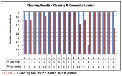
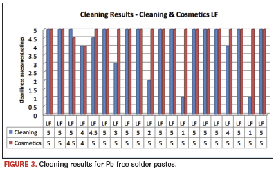
The chosen solder pastes are a representative sample of currently used products in the industry. They included leaded and Pb-free materials, and the investigators chose individual reflow profiles to best simulate real production conditions. Average cleaning results above 4 were considered clean (Figure 2), based on the presence of experimental error, as well as qualitative subjectivity. [Ed.: Comparisons to alkaline cleaners also were made and will be presented at SMTA International in October 2010.] Also, this assessment was supported by additional ion chromatography data on numerous substrates. The pH-neutral product at 10% concentration achieved results of 4 and above in 34 of 40 pastes. This equates to 85% of all tested cases. Four pastes achieved a rating of 2 or below. Increasing the temperature to 160ºF improved the cleaning results to 39 of 40. This constitutes a remarkable 97.5% of all cases tested. It should be noted that visual cleanliness does not necessarily indicate ionic cleanliness, but visible residues generally do indicate residual ionic contamination. Therefore, the only grade on this scale that could be considered a “pass” is a 5. Several areas assigned a score of 5 were confirmed clean with ion chromatography. Scores of 4 or more indicate that the reflow or cleaning process could likely be dialed in to produce acceptable results. Scores of 3, 2 or 1 are unacceptable process failures. Figures 2 and 3 show the cleaning results for leaded and Pb-free solder pastes.
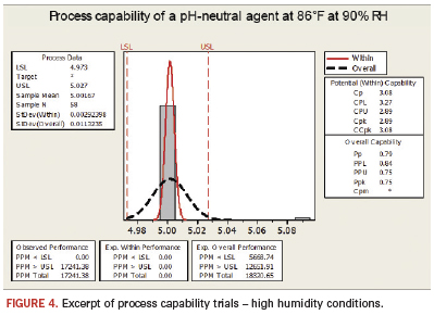
These findings are significant, as for the first time pH-neutral agents have demonstrated cleanliness levels equivalent to those of pH-alkaline cleaning technologies. PH-neutral cleaning agents do, however, add a new level of material compatibility and ease of effluent treatment to the equation. These results truly showcase the future of aqueous defluxing chemistry. Figure 4 shows results of a recent evaluation of the pH-neutral cleaning agent in a high-end inline cleaning process at a provider of comprehensive electronics design and production. Conditions were set at 86°F/30°C and 90% RH in a test chamber. The figure shows the defined process limits, as well as the range of results that passed the test. Eighty-eight boards were tested under the same high humidity conditions. One board failed the high humidity conditions, as the assessed readings did not deliver values according to the customer’s specification.
Flux residues and impurities under low-standoff components are often difficult to remove, since not all water-based cleaning agents are designed to enter this minimal gap between package and board. Therefore, cleaning agent entrapment becomes a common issue: The cleaning agent is not properly rinsed away after application, and impurities together with cleaning agent residues are trapped under low-standoff components or around solder joints, making PCB boards more vulnerable to creeping and long-term corrosion. This, in turn, can cause failure, including field failures. Studies are underway to further examine dissolved flux residues and their respective effect on contributing to corrosion. Generally, it is commonly understood that pH-neutral defluxing technologies can limit these risks of corrosion underneath components, while providing higher levels of material compatibility.
Acknowledgments
Zestron thanks Ersa for its generous support with the Hotflow reflow oven, and Speedline Technologies for its generous support with the Aquastorm AS 200 cleaner.
References
1. F.R. Cala and A.E Winston, Handbook of Aqueous Cleaning Technology for Electronic Assemblies, Electrochemical Publications, November 2005, pp. 64-65.
2. IPC-A-610E, Acceptability of Electronic Assemblies, April 2010. http://www.ipc.org/4.0_Knowledge/4.1_Standards/revstat1.htm
3. IPC-TM-650, method 2.3.28, Ion Chromatography - Dionex ICS-1100, http://www.ipc.org/4.0_Knowledge/4.1_Standards/test/2.3.28A.pdf.
Bibliography
1. Chrys Shea, “Under Component Cleaning – How Low Can You Go?” CIRCUITS ASSEMBLY, July 2010.
2. Zestron Europe, “Reliable Coating with Proper Cleaning - Cleaning Process Benefits for EADS.” Process Cleaning Magazine, January 2009.
3. Dr. Harald Wack, “The Future of Cleaning OA fluxes,” SMT, September 2009.
4. Zestron in cooperation with AAT, “Thermal Residue Fingerprinting: A Revolutionary Approach to Develop a Selective Cleaning Solution,” APEX 2009.
5. Zestron, “Fluid Flow Mechanics: Key to Low Standoff Cleaning,” IPC Midwest, 2008.
6. Dr. Harald Wack, “Eutectic and Lead-Free Defluxing in One Single Process,” SMT, March 2007.
7. Umut Tosun, “Cleaning Lead-Free Prior to Conformal Coating? Risks and Implications,” IPC Apex, February 2006.
8. Andreas Muehlbauer, Ph.D., “Are Lead-Free Assemblies Specifically Endangered by Climatic Safety?” IPC Apex, February 2004.
Harald Wack, Ph.D., is president; Joachim Becht, Ph.D., is head of R&D; Michael McCutchen is sales and marketing manager; and Umut Tosun is application technology manager of Zestron America (Zestron.com); h.wack@zestronusa.com.

Press Releases
- Zollner Puts a New Mechanics Building into Operation
- Changes in Incap’s Management Team: Incap updates its leadership model to support its growth strategy
- Niche Electronics Celebrates Completion of Florida Expansion
- Microscreen Names Nik Thomas Director, Expands Leadership Role Amid Continued Organizational Growth