


What happens when the “world’s workshop” runs out of workers?
Ask someone in our industry, or any industry, for a short slogan describing the Chinese manufacturing juggernaut and you might hear phrases like immense capacity, unfair monetary practices, government-supported, environmental concerns, unfair trade practices, or a host of other admittedly pro-Western sentiments. But I never thought I would live to hear the term labor shortage used about China.
How could a land of well over one billion people lack the workers to fill positions in its manufacturing sector? Because it appears that is exactly what is happening.
I just returned from Taiwan and China and was surprised to hear from every customer, vendor and supplier that the local labor shortage is putting pressure on almost every sector of the Chinese manufacturing landscape. At the beginning of my trip, I had a single purpose for each firm that I visited. But after hearing about this issue during my first stop, I made a point of focusing on it with each successive visit to areas in Hong Kong (or more specifically, Guangdong Province), Suzhou, Shanghai and other locales.
For the past decade or so, business conditions in China have closely resembled those of mid 18th century America. Most US businesses at that time were located along the coastal regions of the Northeast. Close proximity to waterways helped early American businesses quickly move products from factories to a wide range of customer locations. It took many years for sufficient infrastructure to develop so that business could move into the interior states and still have economically feasible ways of getting newly created product to market. As business moved inward, population shifts began to occur as people followed jobs and commerce westward.
In China, commercial development was also a coastal phenomenon, beginning on a large scale in the areas between Hong Kong/Kowloon and continuing up the coast to Shanghai.
A major difference, however, between the early US and Chinese models is where the labor force originated. In China, prior to the great move toward capitalism, most people lived in rural areas. (Hong Kong, before it was turned over to China by the British, is the exception.) But then many Chinese people left their farms and home provinces and moved to urban areas in search of better jobs and a better life. The Chinese businesses in the coastal cities had a plentiful and ever-growing labor supply.
But whereas in the US, part of the labor force located on the coast moved inland with businesses and then established permanent communities there that spanned generations, many urban Chinese still considered their traditional rural provinces “home.” And now that manufacturing is exploding across China, thousands of companies are setting up shop inland, where the infrastructure is in place to permit efficient movement of product, and province-to-province mobility – once restricted by law – is being eased.
With the home provinces now offering a plethora of employment opportunities, a great exodus of people who moved to the coast searching employment are now looking homeward for a similar position closer to family and friends.
As with all good ideas, once the word gets out, many people will try the same thing. The difference is that in China, the effect is multiplied a thousand-fold.
I have been told the exodus began first in the Greater Shanghai region, then moved down the coast to Hong Kong. The Chinese New Year gave many people a perfect opportunity to make the move as part of the holiday’s custom of returning to one’s birthplace. Thus, a labor shortage that no one would have predicted just a few years ago has suddenly taken hold.
I heard about this problem from those involved in the PCB industry, but could easily envision this phenomenon spreading to other industries as well. The customers and vendors I queried estimated that between 800,000 and 1.3 million people have abruptly left their jobs and moved from the coastal areas. This has created a huge vacuum in some businesses in the affected areas. Trained workers are now in short supply, and the hiring pool has shrunk to a level not seen before.
One might think that replacing workers in China would be easy. Not so. One of my customers ran a job ad for workers for a month and received only one response.
This applicant was quickly hired, but left soon after as another, slightly better position opened up. All the people I spoke with expect the labor issue to ease at some point, but because of the enormity of the issue, none would estimate when things would get better. In other words, no quick fixes are on the horizon. Workers will need to be hired, trained and paid well enough to prevent them from moving to competing employers.
One reaction to this problem has been to send a lot of PCB manufacturing back to Taiwan. This influx of work has created a logjam in Taiwanese board houses and is creating a laminate shortage as everyone scrambles for material to manage the increased load. This is not a sustainable solution.
I didn’t think much could surprise me in this industry, but a labor shortage in China did come as a shock. Given the current dismal employment picture in the US, we may well wish we had China’s problem. But a labor shortage there is likely to affect a wide range of Western industries dependent on Asian manufacturing capabilities, just when our own much anticipated recovery is underway. It’s a trend worth watching.
Tom Coghlan is operations director at Bare Board Group Inc. (bareboard.com); tom@bareboard.com.

iNEMI’s new leader is charging far and wide to further the consortium’s green plans.
It’s been a whirlwind debut for Bill Bader. Named last fall as the second chief executive in the 15-year history of iNEMI (inemi.org), he came from Intel with an impressive background in packaging, assembly and experience overseeing hundreds of employees. Since then, he’s traveled the globe, meeting with members and project leaders and absorbing the 70-member consortium’s somewhat divergent views on the industry. He spoke with CIRCUITS ASSEMBLY’s Mike Buetow in a pair of interviews in April and May.
CA: How have you been spending your time of late?
BB: At the end of 2009, 75 to 80% was programming, and 20% member updates. In November we held an environmental meeting in Europe and were invited to present at a ChemSec meeting on RoHS in Brussels. [Ed.: The International Chemical Secretariat, or ChemSec, is a nonprofit organization whose goal is a toxic-free environment.] Sixty-two people attended, about 10 from non-government organizations. It covered halogens, materials, eco-design, sustainability and recycling.
CA: In your opinion, how up to speed are the NGOs on the impact of large-scale materials transitions?
BB: Several, including ChemSec are on top of the materials, very well informed. Some of the others know what’s going on, but the methodologies are sometimes questionable.
CA: What was iNEMI’s role at that conference?
BB: The game plan was to inform the community about the technical issues when you rapidly transition materials content for PCBs, cables, connectors and what we are doing on that.
Likewise, we participated in a packaging workshop in Japan. Fifty people attended. This was to stimulate discussion on key technical issues in the packaging field. Japanese companies classically like to do their own R&D. They did agree, however, to collaborate on warpage issues. There is some real work to be done on this, including developing appropriate standards and specifications.
CA: Is this an area where iNEMI would actually write its own standard?
BB: By definition of our bylaws, we are not allowed to write standards.
CA: What are some of the other key programs right now?
BB: We have task forces on alternative energies and medical electronics. Both have serious needs for standards to drive technologies and cost efficiencies. This fits our competencies. What iNEMI does well is the engineering work required to define best approaches and methods, and subsequent standards and specs.
CA: You’ve been on the job about nine months. What do you think so far?
BB: I like it. [Smiles.] The people you interact with are great. So are the opportunities to make a difference. We have great things started in packaging and miniaturization. For example, we’re working on four new initiatives to address gaps in organic substrate technologies: warpage factors, warpage qualification and modeling, wiring density and holistic modeling. For the last one, we want to develop a design tool to optimize package design in terms of electrical, mechanical and thermal performance. We are working to engage globally in key research priorities with technical organizations like the Fraunhofer Institute in Germany and Peking University in China. We established leadership committees to help us identify the next focus areas of interest and need. When we get all these efforts running smoothly and efficiently, we will really grow our value for our members. All of these efforts are making excellent progress.
CA: What are the problems you did not foresee?
BB: When critical leaders of projects get pulled away. We have to keep the communication lines open.
CA: How does iNEMI set its goals and priorities?
BB: We put together a Leadership Steering Committee made up of some of the highest level companies in the environmental area that could identify the priorities and identify methodologies to affect the speed of execution of those priorities. That team was put into place shortly thereafter. We held some meetings in April to set out priorities and objectives for the future, including where we are going to engage. On that committee, there are eight member companies: six OEMs, one academic institution and one supplier that’s an environmental leader in its industry. OEMs tend to lead in this area, and suppliers tend to take their lead. That’s one example of how goals are set. There is also strong interaction with our board.
CA: Characterize iNEMI’s priorities in the environmental arena.
BB: One key focus area is halogen-free. [iNEMI defines halogen-free as less than 1000 ppm]. We are doing all the necessary engineering work to qualify mechanically and electrically acceptable alternatives to halogenated circuit boards that have the necessary mechanical characteristics from a mechanical standpoint – rigidity, flexibility, solderability – and, electrically, meet the signal buss speeds of the future as necessary to support high-end computer products. We call this our HFR-Free PCB Materials Project. The objective is to get alternative materials qualified and ready to design into new projects by late 2011. There just are not drop-in replacements for high-speed, high-performance products. There’s a lot of engineering work to be done. What we are looking at from our HFR-Free team are eight to 10 alternatives for PCBs. To do the design of experiments, test sample sizes on eight to 10 different materials on a worst-case (most demanding) design situation; that amount of work is very significant. What an OEM gets as an advantage is its research load is probably 1/20th of what would be involved by itself. It’s a shared workload opportunity. The other reason there’s good collaboration environmentally is many of our key OEM members are looking for a level playing field. If in fact all companies are required to deliver halogen-free PCBs with truly better engineering, they are fine with that. That’s not where [OEMs] see their marketing advantage. If we can affect how legislation such as RoHS happens as a function of having an industry-wide backed position, that’s great.
Another focus area is Product Carbon Footprint. We published a position statement on this on March 1, to articulate the membership position on how product carbon footprint methodologies and capabilities should be pursued from an industry standpoint. There is a tremendous opportunity for industry to affect the carbon footprint in the world.
With that release, we are supporting two projects to get the effective tools and methodologies in place. An internal development is the Eco-Impact Evaluator, which is a method for developing an information database using a building block approach. It’s creating a library and database of info where any designer of an ICT product could take information out of the database and define what their project will look like. The database will have a list of environmentally friendly materials. It’s being led by Cisco and Alcatel-Lucent.
A second project we support, one being led by MIT, is a lifecycle analysis toolset. This is for laptops initially, but will expand to other computers. It is similar to the Eco-Impact Evaluator, but much more specific in the short term. So for carbon footprint, we’re working on defining how it should be measured and used and developing tools to support it.
Another project in place is the PVC-free material alternatives for power cords for computers. We’re doing the engineering and evaluation work for a number of material options for resin and plasticized compounds that meet UL 94V0.
CA: How are you presenting all this to the outside world?
BB: We’re taking a number of approaches. We hold workshops for engaging people outside iNEMI, such as NGOs or legislative groups. We have a workshop scheduled in July at Purdue University centered around defining environmental priorities and projects that would be worked on by a university research center, which Purdue has defined in a grant. There are global aspects to that too; others that are interested are Catholic University in Belgium and several universities in the Far East.
There’s PINFA (the Phosphorus, Inorganic and Nitrogen Flame Retardants Association), a consortium of chemical suppliers doing cooperative research on alternatives for flame retardants. We’ve created an in-kind membership.
The next one may or may not happen. I’m going to Europe in June for a workshop meeting, and have made a request to meet with Greenpeace in an open, transparent mode to share what we are doing. And I haven’t decided what title to put on this, but it’s a working session by invitation only for industry stakeholders, including customers, legislators, and NGOs to critique best methods for effective environmental improvement. We will invite industry leaders from parallel industries as well.
Those are things we have done and are in process. We are committed to doing an environmental update newsletter on a quarterly basis to foster transparency and open the communication channel.
CA: What do you do about the maelstrom of paperwork?
BB: We are trying to stay on top of it. It is very, very challenging. One way is through an in-kind agreement with a database company called Compliance and Risks. Based in Ireland, they created a search system based on a real-time, up-to-date database that stays on top of all the regulatory actions in the world. They are funded by an impressive set of member companies. They put in their database all the information from the reports that occur in the EU, China or the US, new laws that come out from the state of California, etc., so you have in one place a searchable database of all info that is published in the world at large. We are a data partner, so we provide them with information and have access to the full database.
The second way is through the regular review of the projects we are running, where we ask, What’s new in the world, and are we working on the things we need to do, or are they changing? It never stops and the lights never go out.
Using laser alignment and novel placement force control, accuracy of 50 µm at 4-Sigma is achievable.
After 20 “static” years, more realistic measures are needed.
In the late 1970s, with the advent of large-scale integration (LSI), ESD started to become a problem. Electronics manufacturing companies soon started to implement ESD control programs. At first, there was little information sharing and no ESD control standardization. Early standards focused on ESD risks from people and on ESD protective packaging. Standards for ESD control items, such as wrist straps, work surfaces and flooring followed as improvements to ESD control materials and equipment were made. In 1999, the ANSI/ESD S20.20-1999 standard for ESD process control was published. A third-party certification program was established to demonstrate compliance with the standard. Eight years later, updated versions of the ANSI/ESD S20.20-2007 and IEC 61340-5-1:2007 standards were published. Facilities compliant with these standards expect to be able to handle devices down to 100V for the Human Body Model (HBM) without significant problems. In this context, adding ESD protection to bring device ESD withstand to 2kV HBM seems to be a case of over-engineering.
In the early days, devices had relatively small numbers of pins and were assembled largely using manual processes in relatively uncontrolled ESD environments. The likelihood of large amplitude HBM ESD events occurring to pins was relatively high. Over time, the number of device pins has increased dramatically, as has the level of manufacturing automation. Many devices can only be assembled in automated manufacturing systems, and ESD control has greatly improved. The likelihood of large amplitude HBM ESD has significantly reduced in these manufacturing processes. However, the number of protection networks required, and chip area they occupy, has grown along with pin count. Device ESD susceptibility test time and difficulty has increased correspondingly. When devices fail to meet the targets, the price of redesign can mean months of delay to product introduction. The ESD targets are particularly difficult to meet on high performance (e.g., low leakage or high-speed) pins. ESD protection networks add capacitance and leakage paths. At 45 nm and 32 nm technology, 18 Gb/s cannot be met with 2kV ESD protection, but can be with 1kV or less.
The potential benefits of reduced ESD target levels are clear. These include savings in design time and effort, faster release of production devices, accelerated and easier improvements in device performance and reduced chip area occupied by ESD protection networks.
Since the mid 1980s, it has been industry practice to supply ICs with ESD protection, where possible, to meet 2kV HBM ESD. While IC suppliers make every effort to meet these established ESD target levels, customers tend to expect these same levels without exception for product qualification. There is really no concern from either side, as long as these de facto levels are met. However, many quality and product engineers observe, with increasing frequency, that the advanced IC products have been encountering product qualification delays at every advanced technology node. At the same time, numerous products have been shipped with ESD protection on some pins at lower levels (after agreement with customers) to achieve desired performance. Despite this, field return rates have not been observed to be different from the products shipped at, or exceeding, the normal target ESD levels. These observations clearly indicate the target ESD levels must be considerably higher than necessary. Even more important, it leads to the conclusion that these levels could be universally reduced with no outside impact, while allowing the design freedom necessary to meet the technology advances.
Consolidated studies. To investigate and establish the true nature of these initial observations, a consortium of ESD experts known as the Industry Council on ESD Target Levels was launched in 2006. This council mainly consists of IC suppliers, consultants, contract manufacturers, and OEMs. It conducted massive studies on the existing ESD control methods and their relation to field return rates of IC products shipped at different ESD levels. The main conclusion was that with the basic mandatory ESD control methods practiced at every production area, products shipped at 500V HBM design levels are just as safe as products shipped at 2kV HBM levels. This is a clear confirmation that the current 2kV HBM target is an over-specification and that reducing this to 1kV should not have any impact on the customer qualification requirements.
With the introduction of recommendations on more practical, but still safe ESD protection target levels, some customers naturally show concern that there could be hidden impact on the reliability of the whole system itself. That is, while product yields may be unaffected, systems using these components might start showing unexpected failures in operation due to reduced ESD immunity. First, this concern arises from a misconception that the HBM component ESD test method represents the stresses that happen in a system environment where ESD transients are actually remarkably different in nature. Second, the data gathered by the Industry Council did not show any evidence of increased return rates from customer applications at 500V compared to 2kV HBM rated parts. The second fact naturally follows from the arguments from the first. The third, and most important, point is that electronics systems in operation require special protection strategy independent of the component-level ESD protection. Component-level protection is driven solely by the need to prevent damage during handling in the production area. So, component-level protection changes should not warrant a concern for system-level protection, provided the proper system protection is designed and followed. These same arguments also apply for Electrical Overstress (EOS) failures, which are independent of component-level ESD protection. All of these observations have been fully documented in a white paper published by the Industry Council.1
Epilogue: Since publication of the recommended HBM target levels, the Industry Council also has conducted detailed studies of charged device model (CDM levels). As a complement to HBM, CDM represents metal to metal discharge from the package leads and is an important ESD specification. For CDM, the industry de facto standard has been 500V. However, rapid advances in silicon technologies, high-speed circuit designs and IC package advances are making it virtually impossible to meet this level for many of the large pin devices with high-speed serial link designs at the 45 and 32 nm nodes. Similar to HBM for human handling, production area CDM controls to prevent metal to metal discharges have progressed far enough to safely recommend lowering this target to 250V.2 Both HBM and CDM requirements have been documented as JEDEC white papers.
The time has come for ESD target levels to be changed for the sake of the industry. IC suppliers should always guarantee the recommended minimum ESD levels are achieved. Electronics system manufacturers should diligently follow ESD control methods, according to standards such as IEC 61340-5-1 and ANSI/ESD S20.20, to prevent ESD damage during component handling and assembly in production areas. A general appeal is made to IC customers to keep component ESD protection level requirements at a realistic perspective and adopt the recommended new ESD target levels.
The Industry Council intends to publish a new white paper on effective system-level protection. This is an important subject, but should not be tied to component ESD levels.
Without these common goals, IC technology will continue to run into roadblocks during ESD qualification. With a common approach and better communication, a balanced ESD strategy can be achieved. The most important initial step is to remove the barriers by recognizing that new ESD level changes are urgently needed.
References
1. JEP155, Recommended Target Levels for HBM/MM Qualification, esdtargets.blogspot.com.
2. JEP157, A Case for Lowering Component Level CDM ESD Specifications and Requirements, esdtargets.blogspot.com.
Dr. Charvaka Duvvury of Texas Instruments (ti.com) and Dr. Harald Gossner of Infineon Technologies (infineon.com) are co-chairs of the ESD Industry Council (esdtargets.blogspot.com); c-duvvury@ti.com. Dr. Jeremy Smallwood is a consultant at Electrostatic Solutions Ltd. (static-sol.com).
In Case You Missed It
Chip Assembly
“Complex Self-Assembled Patterns Using Sparse Commensurate Templates with Locally Varying Motifs”
Authors: Joel K. W. Yang, Yeon Sik Jung, Jae-Byum Chang, R. A. Mickiewicz, A. Alexander-Katz, C. A. Ross and Karl K. Berggren; berggren@mit.edu.
Abstract: Here, we show that an array of carefully spaced and shaped posts, prepared by electron-beam patterning of an inorganic resist, can be used to template complex patterns in a cylindrical-morphology block copolymer. The authors use two distinct methods: making the post spacing commensurate with the equilibrium periodicity of the polymer, which controls the orientation of the linear features, and making local changes to the shape or distribution of the posts, which direct the formation of bends, junctions and other aperiodic features in specific locations. The first of these methods permits linear patterns to be directed by a sparse template that occupies only a few percent of the area of the final self-assembled pattern, while the second method can be used to selectively and locally template complex linear patterns. (Nature Nanotechnology, April 2010)
Embedded Components
“Industrial PCB Development using Embedded Passive & Active Discrete Chips Focused on Process and DfR”
Authors: M. Brizoux, A. Grivon, W. C. Maia Filho, E. Monier-Vinard, J. Stahr and M. Morianz; michel.brizoux@thalesgroup.com.
Abstract: This paper discusses aspects of the PCB embedding technology developed in the frame of the HERMES project (High density integration by Embedding chips for Reduced size Modules and Electronic Systems). This European-funded FP7 three-year research program targets to establish an industrial platform capable of producing PCBs with two layers of embedded components, including large die sizes. The embedded PCBs manufactured were populated with external SMD components on both sides to constitute complex high-end integrated modules able to withstand conventional repair operations and ensure a high-reliability. (IPC Apex, April 2010)
Organic Electronics
“Influence of Dielectric Surface Chemistry on the Microstructure and Carrier Mobility of an n-Type Organic Semiconductor”
Authors: Parul Dhagat, Hanna M. Haverinen, R. Joseph Kline, Youngsuk Jung, Daniel A. Fischer, Dean M. DeLongchamp, Ghassan E. Jabbour; deand@nist.gov.
Abstract: Organic electronics, use carbon-based materials that are intrinsically semiconductors. This paper examines the microstructure evolution of 3,4,9,10-perylene-tetracarboxylic bis-benzimidazole (PTCBI) thin films resulting from conditions imposed during film deposition. Modification of the silicon dioxide interface with a hydrophobic monolayer (octadecyltrichlorosilane (OTS-18)) alters the PTCBI growth habit by changing the unit cell contact plane. PTCBI films deposited on oxide surface have an orientation of (011), while films atop OTS-treated oxide surface have a preferred orientation of (001). The quality of the self-assembled monolayer does not appear to influence the PTCBI growth preference significantly, yet it enhances carrier mobility, suggesting that charge traps are adequately passivated due to uniform monolayer coverage. High-quality monolayers result in n-type carrier mobility values of 0.05 cm2V-1s-1. Increasing the substrate temperature during PTCBI film deposition correlates with an increase in mobility that is most significant for films deposited on an OTS-treated surface. (Advanced Functional Materials, Aug. 3, 2009)
Solder Joint Inspection
“Robust Automated Void Detection in Solder Balls and Joints”
Authors: Asaad F. Said, Bonnie L. Bennett, Lina J. Karam, and Jeff Pettinato; asaad.said@asu.edu.
Abstract: A robust, accurate and automatic void detection algorithm is proposed. The proposed method is able to detect voids with different sizes inside the solder balls, including the ones occluded by board components and under different brightness conditions. The proposed method consists of segmenting individual balls, extracting occluded balls and segmenting voids inside the solder balls. Segmentation of individual balls is achieved by using the proposed histogram and morphological-based segmentation method. A voting procedure is used to segment the occluded balls where the pixels inside the occluded area are checked to obtain candidate pixels representing the occluded joint’s or ball’s centroids. An independent edge-detection procedure is used to get candidate voids inside individual balls. Mathematical morphology operations are used to locate all possible valid voids and remove non-void areas. The proposed algorithm was applied to three different Intel products. Results were compared to results obtained by an automated algorithm in an existing state-of-the-art 2D x-ray inspection system, results obtained by trained operators from 2D x-ray images, and results obtained by trained operators from 3D CT scan images. The results (pre SMT solder balls) show the proposed method is capable of successfully locating all possible visible voids inside the solder ball, even ones missed using other methods, as well as those hard to see by the human eye. (IPC Apex, April 2010)
New Techniques to ID Counterfeit ICs
Acoustic micro imaging can reveal whether the die and lead frame are genuine.
SMT Corp. is an independent component distributor. To prevent counterfeit plastic-encapsulated ICs from reaching its customers, it uses multiple detection technologies, including visual inspection, light microscopy, digital stereo microscopy, resistance to solvents testing (RTS), scanning acoustic micro imaging, real-time x-ray, acid etch and mechanical decapsulation for die verification, solderability testing, BGA coplanarity inspection, scanning electron microscopy (SEM), energy dispersive spectroscopy (EDX), and x-ray fluorescence (XRF) inspection. Components identified by SMT as suspect-counterfeit are either turned over to federal law enforcement, government agencies, the IP holder, or ground up onsite and environmentally disposed.
A practical necessity in any method of counterfeit identification is the availability of known genuine components of the same type. Except in instances of truly outlandish components (misspellings on the label, no die in the package, etc.), having genuine parts for comparative analysis makes counterfeit identification much easier, especially in components where some features fall in a gray area. (Are those delaminations extensive enough to prove counterfeiting, or are they just unusually sloppy work by the OEM?)
Component users encounter two different types of counterfeit parts. By far the most common is the “recycled” ICs that began life, generally five to 15 years ago, as a new, genuine component from a legitimate component manufacturer. Eventually the circuit board it resided on was scrapped and shipped offshore, where the entire component population was burned off for refurbishment, remarking, repackaging and reintroduction as new into the global supply chain. SMT Corp. estimates recycled ICs comprise 80 to 90% of all counterfeits currently in circulation worldwide.
A small percentage of counterfeit components are “made-from-scratch” – or knock-offs. A foreign counterfeiter with component manufacturing capability finds it worthwhile to replicate the entire component altogether – and does so without the permission of the original IP holder. The chip and other internal features may be nonfunctional or even absent, or – worse yet – functional!
The vast majority of recycled counterfeits undergo a process something like this: The board is heated in an uncontrolled harsh environment (usually an open-flame fire) until solder reflows, at which time the board is smacked against a hard surface to remove the components. The components from hundreds or even thousands of similar boards are collected and washed (sometimes in a nearby river, sometimes outside in the rain) to remove residue from the high-heat removal process, and then sun-dried. Most are then rough-sorted by sifting and then hand-sorted by part number or similar package style. In many cases, components of different manufacturers, vastly different functions and electrical characteristics wind up in the same finished counterfeit lot, as long as they have the same number of leads and the same package dimensions.
The original component part markings are then removed (generally by rubbing the component by hand against sandpaper tacked to a table). A “blacktop” coating that more or less approximates the texture and color of the original mold compound surface is painted or sprayed onto the component’s top surface to cover the sanding marks. Last, the top surface is reprinted (remarked) with a legitimate-looking manufacturer’s logo, part number and more recent lot/date code. They are then packaged in what looks like (and may actually be) authentic original component manufacturer (OCM) packaging and offered for sale as new product direct from the manufacturer.
The longevity of functioning counterfeits is, of course, questionable indeed. It should be pointed out, given the huge volume of containers recycled each year, that it is perfectly possible for the same component to be recycled multiple times. For the successful counterfeiter, external appearance of authenticity at the point of sale is what matters most; downstream functional issues become someone else’s problem.
The efforts of counterfeiters to mimic the appearance of genuine components involve considerable innovation. While some methods are still crude, many are not.
In July 2009, SMT Corp. was the first to identify a new, harder to detect blacktopping material that, when applied carefully, looked almost identical to the OCM’s top coating. Traditionally the paint-like blacktopping material has easily been identified by a solvent swab of pure acetone, or even a much milder 75/25% mixture of mineral spirits and alcohol. These solvents would dissolve the traditional blacktop coatings and reveal visual evidence left behind by the counterfeit process of removing original part markings.
This new advanced blacktop material is harder to distinguish visually from the surface of a genuine part, and is not affected whatsoever by traditional RTS test methods. An engineer applying traditional solvent testing would conclude it to be a genuine part. SMT believes this advanced blacktop material is made from the dust ground off components and then mixed with a heat-activated epoxy compound before being sprayed on and heat-cured for hardness and durability. In September 2009, Honeywell Aerospace shared its process using a heated solvent called “Uresolve” (made by Dynaloy) that proved effective in removing the new blacktop coating from counterfeit components. The only major drawback to the process was it also could remove the topcoat that OCMs put on the majority of authentic components. (Factory-applied topcoats, like the blacktopping that counterfeiters use, can be scraped off with a razor, but they hide no
sanding marks.)
In January, SMT Corp. further refined that process using a different Dynaloy product called DynaSolve 750. After considerable experimentation on a wide range of counterfeit and authentic parts, a temperature/duration process was identified that completely removed the new blacktop (exposing the sanding marks below) – yet had no effect on the factory-applied topcoats of all authentic components tested. The refined process required the DynaSolve be preheated to 105°C and the suspect component to be half-immersed for 45 min. (Figure 1).
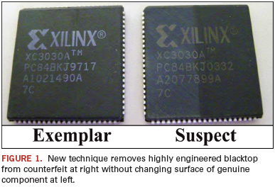
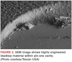
These same components showed other signs of counterfeiting as well. For example, the highly engineered blacktop material had been sprayed onto the top surface, and some had visibly coated the upper portion of the side of the component. In addition, the blacktop material had in some cases been sprayed into the pin-one cavities, with the result that the cavities in close optical view appeared roughly textured rather than perfectly flat and smooth. Figure 2 is a SEM image of a portion of one pin-one cavity that has been partly sprayed. Some cavities, however, were completely clean and resembled those found in genuine parts.
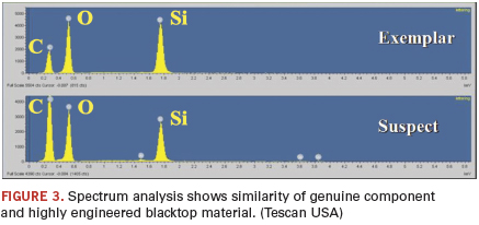
EDX analysis compared the results of the new blacktop material with analysis of the top surface of known genuine components. The results
(Figure 3), while not identical, suggest it is possible that the sprayed-on blacktop had its origins in the dust created by sanding genuine components.
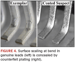
Another clue was found in the leads of the components. At left in Figure 4 is a light microscope view of two leads from a genuine component. Because these leads were straight when coated, the forming process produced some cracking or scaling of the coating at the bend. This is an expected feature on genuine components. But counterfeiters apply coatings to leads that are already bent, so cracking and scaling are absent. The coating applied by counterfeiters also rounds off the lead ends and conceals the copper base metal visible in the cut-off lead ends on the genuine parts.
Most acoustic methods developed by Sonoscan use VHF or UHF ultrasound reflected from material interfaces at a depth of interest such as the die surface, the lead frame of die paddle surface, or the die attach depth. For example, when imaged acoustically, both genuine and counterfeit components treated with DynaSolve at 105°C show some internal delaminations at the lead finger depth not present beforehand, an indication that the test should be
considered destructive.
The same C-SAM acoustic micro imaging system that images internal features can also image surfaces acoustically. It can also characterize a material at the same time it is making an acoustic image.
One of the oldest methods for spotting possibly counterfeit components is the simple application of a single pulse of ultrasound to determine the mold compound’s acoustic impedance (acoustic velocity times density, the product expressed in megarayls). If known genuine parts have an acoustic impedance of around 4.3 megarayls, and an incoming part has an acoustic impedance of 7.6 megarayls, the new part may be a counterfeit, or the legitimate supplier may be using a new mold compound. One recent development: Some made-from-scratch counterfeiters are selecting mold compounds that attempt to match the acoustic impedance of the genuine component.
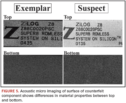
During acoustic imaging of components, it is customary to scan the top surface of the part by itself for reference. The surface image gives no information about features at depth, but it turns out to have value in identifying counterfeits when the bottom surface, which is ordinarily not of interest, is also imaged. In genuine components, both surfaces appear identical acoustically because they were formed from the same material during the same injection molding process. But in a recycled fake where the top has been blacktopped, the two sides often look very different. (Figure 5).
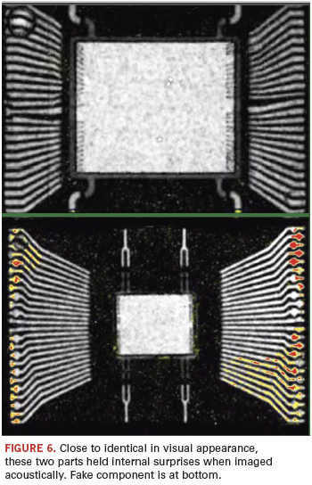
When an acoustic micro imaging system targets a specific depth within a counterfeit, strange things are sometimes found. Figure 6 shows two outwardly identical components having the body dimensions, the same label and the same number of leads. But the acoustic image shows that the component at bottom is either a newer die revision from the manufacturer utilizing a smaller die or is from a different component manufacturer altogether and uses entirely different die and lead frame. It also has small delaminations (red and yellow) on nearly all of the lead fingers.
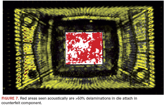
One of the areas of interest in any acoustic image of a component is the percentage of delaminations or similar defects in the die attach material. For example, J-STD-020D, sec. 6.2.1.1, specifies that metal lead frame components may have “no delamination/cracking >50% of the die attach area in thermally enhanced packages or devices that require electrical contact to the backside of the die.” New, genuine components may have some percentage of delamination and be perfectly acceptable for most applications. Recycled components may show a relatively greater degree of delamination, presumably because of the thermal and mechanical stresses of prior use and of the counterfeiting process itself. Figure 7 shows the acoustic image of a known counterfeit component whose die attach delaminations (red areas) exceed the standard. Digital image analysis showed delaminations covered 57.12% of the die attach area.
It may be difficult to tell whether a particular component with above average die attach voiding is simply an isolated item from a good OEM, or whether this component has been heated irregularly, smacked on the ground and washed in a river. Determining whether a part is counterfeit is easier if multiple questionable parts and multiple known genuine parts are available in order to look for patterns. One group of counterfeits seen in Sonoscan’s laboratory had varying delaminations, some covering only part of the die paddle, and some extending onto the die face. The corresponding group of known genuine parts all had smaller delaminations, all on the same corner of the die paddle.
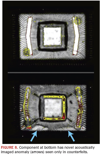
Collaboration between SMT and Sonoscan has resulted in the identification of internal features not previously seen acoustically in components. Figure 8 is the acoustic image of a pair of components. The genuine part at top shows minimal defects. The recycled counterfeit at bottom shows numerous delaminations (red, yellow) on the die paddle and on the tape. But it also shows a surprising feature: two over-bright regions (arrows) near the bottom edge. Something has happened along this edge to make the interface between the mold compound and the lead fingers appear brighter than elsewhere, and the upper edge of this phenomenon is marked by a dark line. Two possible explanations: Sanding may have altered the top edge of the component, causing the returning ultrasonic echoes to bend; or heat may have re-cured or otherwise altered the mold compound in this region, but without creating a gap (delamination), which would be red or yellow. Strange effects seem to occur when components are subjected to heat, mechanical shock and moisture in uncontrolled environments.
This brief article has not covered all of the techniques currently available to identify counterfeit components, but it demonstrates what may be accomplished with the innovative use of technological resources. Since counterfeiters are actively responding to detection methods, new detection methods will continually be developed to keep counterfeit parts out of production.
Dr. Lawrence W. Kessler is president of Sonoscan (sonoscan.com). Thomas Sharpe is vice president of SMT Corp. (smtcorp.com); tsharpe@smtcorp.com.

Press Releases
- Zollner Puts a New Mechanics Building into Operation
- Changes in Incap’s Management Team: Incap updates its leadership model to support its growth strategy
- Niche Electronics Celebrates Completion of Florida Expansion
- Microscreen Names Nik Thomas Director, Expands Leadership Role Amid Continued Organizational Growth