


Odd-form components and flex circuits are two common applications.
Fixtures typically are needed for nontraditional PCB assemblies. The vast majority of selectively soldered boards enter the machine without fixturing. Odd-form parts, harnesses or wired assemblies, and particularly flex circuits, occasionally need fixturing. For example, some flex circuits must be held flat; one has to “locate” the flex circuit and then hold the components in place for the soldering operation.
Other typical reasons for using fixturing include instances where the board edge clearance is not to SMEMA standards, or if components hang over the edge of the board, as in edge connectors. Another reason might be if a panel of boards is of a particularly thin PCB material, or double scored, or heavy toward the center, the board may need fixturing to hold it flat so that the small solder wave does not contact the bellying of that board.
The process of providing fixturing, straightforward as it may seem, is not the same as providing an accessory or a spare part to accompany a machine. Rather, it is part of a total package, because engineering and process development are part of the overall effort.
Who provides the fixtures? In some cases, the equipment supplier provides the design, which could be 3D modeled to demonstrate how it will work and how it fits on the machine. The supplier also might develop the process, in conjunction with the customer’s process engineering staff, and design the nozzles. Among the programs for 3D modeling and nozzle design is SolidWorks, a 3D mechanical CAD program that runs on Windows. By using the same program for both, the nozzle and fixture together can be easily articulated.
Fixtures, or pallets, generally are machined out of high-temperature composite material impervious to attack by flux chemistries. It is very dimensionally stable when subjected to temperature changes and does not conduct heat very well, a significant advantage. The primary disadvantage of the material, known as Durostone, is that it is very abrasive and hard and therefore difficult to machine.
How many fixtures are needed for an application? A manual-load machine needs a minimum of three; one is being processed while two are being loaded and unloaded. Automated lines may have a dozen or more. Designing a fixture for a particular application generally takes less than a week.
Fixture design and manufacturing requires a real skill set that develops over time and experience. Successful fixture design requires an intuitive understanding about how to build a fixture correctly, in terms of holding, locating, making it effective for soldering, taking into account the flow dynamics of the solder, nozzle shape and effect, and all important considerations.
Today’s equipment supplier needs to be more of a solutions provider, working closely with the customer to provide a complete custom turnkey system that’s engineered to the customer’s specific application and manufacturing requirements.
Alan Cable is president of A.C.E. Production Technologies (www.ace-protech.com); acable@ace-protech.com.

Figure 1. Fixtures use high-temperature composite material impervious to attack by flux chemistries.
Component assembly is ripe for defects. Here’s how to avoid them.
Placement must undergo various checks to ensure components are the correct ones and to locate potential problems. The first check is at the SMT stage (Figure 1). Called a feeder component check, it involves identifying each part on the reels or trays and matching them with the bill of materials. Quality Control checks item number, component size and values, and ensures that what’s called out in the BoM is what’s on the specific reel or tray.

Figure 1. QC technician conducting a feeder component check to verify each part is identified on the tape and reel and matched with the BoM.
After these checks are satisfactorily completed, QC signs off on the manufacturing process instructions (MPI) form. SMT can then run the first-article board so it can go through screen-printing and pick-and-place. When the board goes through pick-and-place, the machine checks components once again. To perform those checks, pick-and-place equipment uses the dimensions of each part by size and the number of leads on the part. The machine also verifies the thickness of each part. Other checks like coplanarity can be performed to check for bent leads on fine-pitch devices.
(Note that different pick-and-place equipment has different options. Not all machines can handle the wide range of component sizes. Sometimes a custom feeder must be ordered to be able to accurately perform placement. Some feeders are difficult to find for a few odd-shaped devices, especially connectors. For the most part, a third-party is called on to make a special feeder for a particular component.)
QC then re-checks that first-article board after it has undergone a placement from the pick-and-place machine, but prior to reflow. Ideally, a first-article inspection (FAI) system is used (Figure 2). This system, programmed to perform a particular inspection on a particular board, checks component markings and, again, matches components with the already programmed golden board. FAI is a major contributor toward eliminating backend rework.
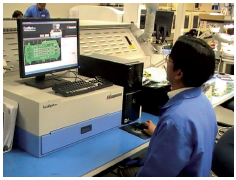
Figure 2. FAI is used after first board undergoes pick-and-place, but before going to reflow to perform another round of checking.
So-called “consigned components” are parts cut from the tape-and-reel and provided to production in an exact number. This is not a good idea: For optimum accuracy, automated assembly needs components in a tape-and-reel. Components from a cut tape must be hand placed and can lead to higher rates of misalignment, bridging or opens.
Further, because there are no markings on these cut tapes at the placement, the wrong components for a job might get mixed in. Having FAI prior to reflow is especially valuable in these instances. As mentioned, floor personnel can check components prior to board reflow to make sure all components are the right ones per the BoM.
Problems also are encountered when components with different values are mixed and placed on trays and bins. Most often, these are salvaged from dead boards and have bent or oxidized leads that could lead to open or insufficient solder after reflow. Avoid salvaged or “pulled” components; they pose reliability issues.
Matching Pad and Package Sizes
Pad designs at the layout stage often present challenges for placement. Sometimes pad designs don’t match the component package sizes specified in the BoM (Figure 3). Consequently, problems arise at placement because the parts are either too big or too small for the pad, resulting in component mismatch. Assembly is halted on that project to report this discrepancy to the customer: The reply usually is to replace it with a different-size component or a notice to not populate that particular component. 
Figure 3. Pad design doesn’t match with component called out in the BoM.
There are countless examples where this discrepancy can occur. Take, for instance, an 0603 part called out in the BoM for a PCB with an 0402 pad design. Assembly issues are encountered when this particular part is placed. An open solder condition is going to result because the 0603 part won’t be able to be placed on that smaller 0402 pad.
Similarly, if an 0402 part needs to go in an 0603 pad design, tombstoning will occur. When a particular side of the part is pulled through on one side, the component stands up (Figure 4) or tombstones. Moreover, there will be open solder and misalignment after this part goes through reflow.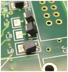
Figure 4. Tombstoning occurs when incorrect pad sizes are used on a PCB.
A BGA pad design with pads of different sizes is the exception rather than the rule at most EMS firms. But occasionally, due either to poor design or fabrication practices, some boards come with different BGA pad sizes. Such situations call for consulting with the customer.
Ideally, BGA pads should be uniformly sized as far as overall PCB pad design is concerned. Assembly personnel do not want to face a mix of small and big BGA pads on the PCB. Such design can lead to open solder conditions and subsequently, latent product problems in the field. Hence, the BGA pad design must be identical to the BGA ball configuration, which is uniform throughout the device.
Unmasking via holes is another associated problem. This creates insufficient solder, especially on a BGA component as it goes through reflow. Here, solder is sucked through the unmasked via hole, thereby creating insufficient or open problems with the BGA. This issue is compounded because conventional x-ray doesn’t spot it, although the equipment clearly sees bridging. (Advanced x-ray machines do see open solder, as well as bridging.)
For successful, accurate placement, PCB designers must interact with assembly and process engineers to ensure the right components are used. They should define and coordinate the various requirements of assembly. In particular, at SMT, PCB designers and assembly engineers must coordinate and place onto the PCB a global fiducial. A GF is used for alignment purposes at screen-printing and pick-and-place. It’s basically a starting point for aligning the solder paste on the board pad. The printer will look for the global fiducial so that it can center boards and apply solder paste cleanly and accurately. A GF is equally important on the pick-and-place machine, specifically for fine-pitch components and leadless devices like BGAs. A local fiducial will help with placement alignment consistency throughout the board, particularly with fine-pitch parts and leadless devices. Assembly and design engineers must coordinate with all these requirements to ensure accurate placement.
Careful design and assembly coordination also involves exchanging detailed information dealing with pad designs. Assembly should provide the design team with a list of components and their matching pad designs. This means matching 0402 parts with an 0402 pad design, an 0603 with a corresponding 0603 pad design, and so on.
Finally, close coordination is essential when dealing with special type or odd-shaped components or connectors. Design and production groups work in tandem to specify and order ahead of time the type of nozzle or equipment needed. Anticipating this need and having special equipment ready considerably helps maintain an OEM’s project schedule, regardless whether it is a prototype or production assembly.
Simon Ilustre is a process engineer at NexLogic Technologies (www.nexlogic.com); info@nexlogic.com.

Novel solder paste formulations overcome miniaturization challenges.
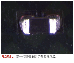
The electronics industry’s never-ending miniaturization quest has constantly challenged conventional processes, forcing solutions to problems that are a direct result of the move to such tight geometries. At the board level, it’s safe to say that a large majority of these issues have to do with the deposit volumes required to achieve high-integrity solder joints for such small components. So, the soldering process – from print through reflow – is front and center. Arguably, however, the move from 0402s to 0201s (with 01005s soon to follow) and from 0.4 mm CSPs to 0.3 mm CSPs into more mainstream production has made some issues even more severe. In fact, this downward trend in pitch dimension has even revealed a new phenomenon not seen before and one that is directly attributable to severe miniaturization: graping.
Graping, as the name implies, is a grape-like cluster formation of partially coalesced solder spheres that make up the solder joint after reflow. Why does this occur? Not only do smaller solder paste deposit volumes call for thinner stencils, more thorough release and smaller solder spheres within the paste material, these necessary miniaturization conditions are also pushing the solder particle surface area to flux ratio to a breaking point. In addition, the surface area to volume ratio of the smaller deposit increases the relative level of surface oxidation.
The primary function of flux is to permit soldering by removing any surface oxides that may be present on metals – including the solder spheres within the paste. The flux will also protect those spheres from re-oxidizing during the reflow process. The move to smaller particle sizes rapidly increases the total metal surface of the solder, requiring more activity. Likewise, smaller deposits will have a higher surface area to volume ratio as compared to larger solder deposits. Since the majority of the powder oxidation is on the particles on the deposit surface, increasing the relative amount of deposit surface increases further the demands on the flux. When the flux can no longer remove the surface oxide, which melts at a higher temperature, then flux exhaustion happens and graping occurs.
A solder material that may reflow very well on 0402s or a 0.5 mm CSP can be significantly challenged on small deposits because there is so much additional powder oxidation due to the increased deposit surface to volume ratio that the flux activity becomes depleted. In these situations, full coalescence does not occur and graping is the result.
Solder paste suppliers address graping through a novel activator chemistry. This helps alleviate the problem in a number of ways. First is ensuring better release from the stencil and more even deposits, thus minimizing the surface area to volume ratio of the deposit. Second is controlling the powder particle size distribution by designing a solder paste that incorporates advanced powder technology. Improved particle size distribution delivers both a reduced metal surface and an optimal deposit surface area to volume ratio. Third is formulating the flux so that it has both sufficient activity and the ability to minimize re-oxidation of the powder, thus overcoming the graping as it occurs. In other words, the flux not only has to reflow nicely on the large deposits, but it also has to be able to remove existing oxides and protect all of the metals from re-oxidizing.

Jie Bai is a chemist at Henkel Electronics Group (henkel.com); jie.bai@us.henkel.com.
Environmental Regulations
“Asian Chemicals Regulations”
Author: Gregory Dripps; gdripps@rohmhaas.com.
Abstract: Asia is adopting core elements of REACH, although the region is not adopting the regulation itself. Registration and reporting are based on tonnage bands, with mandated testing requirements (physical/chemical plus toxicity). Possession of data packages will become a currency of the future as management controls consider a substance’s potential hazards and use, not just hazards. A philosophical shift is underway, whereby the notion that existing or new materials are safe is being abandoned, and comprehensive analysis and testing data are required to demonstrate an acceptable hazard profile. In many nations, rules will go into effect as early as this year. (IPC Symposium on Electronics and the Environment, July 2010)
“Recent Developments in the Implementation of the EU REACH Regulations”
Author: Michael Kirschner; mike@designchain-associates.
Abstract: More than 140,000 substances have been preregistered, almost five times more than expected. To date, there are 38 candidate substances of very high concern (SVHC), and the Commission expects 165 by 2012. Until a listed substance is authorized or restricted, it remains a Candidate SVHC. To use an SVHC, make sure your supplier is legally authorized if your supply chain goes through the European Environment Agency. Furthermore, compliance in the EU does not mean compliance elsewhere. (IPC Symposium on Electronics and the Environment, July 2010)
“Halogen–Free: A Regulatory Overview”
Author: Susan Landry; susan.landry@albemarle.com.
Abstract: Combustion gases generated during fires (whether or not flame retardants are present) that contribute to acute toxicity include CO, HCN, HCl, and acrolein. Carbon monoxide is responsible for more than 90% of all fire-related deaths. The most important pollutants generated in fires are polycyclic aromatic hydrocarbons (PAHs) and polyhalogenated dibenzodioxins and furans (PHDDs/PHDFs). Measurements made in large fires have shown that the PAHs have an up to 500 times higher cancer risk than the PHDDs/PHDFs. PAHs are generated in all fires, and many are carcinogenic compounds. In the US, the “Chemicals of Concern” Action List includes phthalates, short-chain chlorinated paraffins, polybrominated diphenyl ethers (PBDEs), and perfluorinated chemicals, including PFOA. An upcoming DfE will review Deca-BDE alternatives. The Department of Toxic Substances Control is called on to scientifically and systematically identify and prioritize chemicals and consumer products for manufacturers to conduct alternatives assessments, and DTSC could impose regulatory responses for alternatives selected by manufacturers. In June the European Parliament Environmental Committee voted to support amendments that require further evaluation instead of a ban on the use of certain organobrominated materials and PVC in electronics and electrical equipment, with certain exclusions for materials for military purposes and vehicles. (MEPs also called for a ban on nanosilver and carbon nanotubes, and that other EEE material containing nanomaterials should be labeled.) Amendments will now be considered by the full plenary session of the European Parliament. (IPC Symposium on Electronics and the Environment, July 2010)
Laminate Environmental Testing
“The Combustion Testing Phase EPA DfE Project on Flame Retardants for Circuit Boards”
Author: Dr. Emma Lavoie, et al; lavoie.emma@epamail.epq.gov.
Abstract: Goals of this work, a partnership of the US EPA and various industry suppliers, included identifying and characterizing commercially available flame retardants and their environmental, health, safety, and fate aspects in FR-4 printed circuit boards. The work applied lifecycle thinking to consider hazards and exposures, and used EPA New Chemicals Program criteria to evaluate hazard and environmental fate concerns. Methods included comparing the combustion byproducts from FR-4 laminates and PCB materials with different flame retardants during potential thermal end-of-life processes, including open burning, incineration, and smelting. Testing is designed to be a first step in providing industry with a comparative analysis of combustion byproducts from these materials, and to help inform further studies to better understand these byproducts in real-world scenarios. Investigations covered combustion testing of printed circuit board laminates, including materials containing phosphorus, TBBPA and no flame-retardant additives under temperatures of 300°, 700° and 900°C, with and without oxygen. (IPC Symposium on Electronics and the Environment, July 2010) CA
This column provides abstracts from recent industry conferences and company white papers. With the amount of information increasing, our goal is to provide an added opportunity for readers to keep abreast of technology and business trends.

Assembly packaging could mean a bright future.
Conferences around the world are buzzing over the growth projections for high brightness light-emitting diodes (HB LED). In Korea, almost 200 people attended the International LED and Green Lighting Seminar in June, while more than 20,000 people visited the colocated LED and OLED Expo. More than 200 people attended special sessions on LEDs during SemiCon West in San Francisco this past July. Companies are looking at the explosive industry growth, and all hope for a piece of the pie. Strategies Unlimited, Credit Suisse, and McKinsey predict that the LED market – driven by three major applications (general lighting, backlighting, and automotive) – will grow at a 40% CAGR through 2015.
According to the Optoelectronics Industry Development Association, three segments – automotive, lighting, and mobile applications – are expected to grow to 89% of all applications in 2021. What is driving the growth? In the case of lighting, much of the growth comes from pending bans on incandescent bulbs and government mandates that lighting be converted to LEDs for energy savings.
The technology to produce LED die is based on semiconductor diode technology. The emitted wavelength of light depends on the specific semiconductor material used. The key to producing high-quality LED die is the growth of the epitaxial layers and an active p-n junction on an optimum substrate. The p-n junction is critical in determining the device’s internal quantum efficiency (IQE), and the substrate is important because it should match the lattice constant of the semiconductor. The matching lattice constant helps reduce dislocation defects. Dislocation defects can adversely affect the performance of the LED.
Key tools for the growth of the epitaxial layers include MOCVD equipment. Wafers are typically two to four inches with a constant pressure to continue moving to larger wafer sizes.
The packaging and assembly process is also critical to the performance, reliability, and lifetime of the LED product. LED packaging tends to be nonstandard, with every package unique to the supplier.
LED packaging options include use of one large LED die in a package versus multiple die. Advantages and disadvantages are still being debated. It is not clear if one method will dominate or if both solutions will be used. In some cases, multiple die are mounted directly on a metal core substrate or on leadframes.
Thermal issues. Thermal issues have been reported to account for as much as 50% of the failures in lighting. Effectively removing this heat is critical to control junction temperatures of the LED chips, to ensure long device lifetimes, and to maintain the spectral and efficiency characteristics of the light source. Controlling the LED junction temperature (Tj) from 50° to 100°C is critical to LED performance. As the junction temperature (Tj) of the LED changes, the wavelength of emitted light shifts, making color control difficult. If Tj is excessively high, the active region of the LED and the electrodes of the device can degrade, leading to a decrease in the device light output. High Tj can also reduce LED life. Failure to effectively remove heat from the LED source can also degrade the phosphors in the LED package. as well as other packaging materials. Some examples of the latter are yellowing of the encapsulation material and higher absorption losses at reflective surfaces. Depending on the temperature changes, the coefficient of thermal expansion and glass transition temperature of these materials can lead to mechanical stresses that cause failure of the package or the LED die. If catastrophic failure does not occur, these effects often just reduce the lumens output of the package and thus the overall efficiency (lumens per watt) of the source. Excess heat can also lead to premature failure of the LED package from delamination and die fracture.
Packaging materials will also significantly impact the optical efficiency of an LED package. Reflectivity, transmissivity and index of refraction are all materials’ properties that could affect the number of lumens out of the package, and also, the stability of packaging materials (encapsulants and lenses) with exposure to elevated temperatures, UV and other wavelength radiation. As mentioned, elevated temperatures can cause materials to turn yellow, thus reducing the number of photons getting through or changing the color of the light.
The adoption of new technologies is often hyped to the point that unrealistic expectations are created. The story with HB LEDs will be different. The difference with LEDs is that there is a technology pull (the desire for energy efficiency) and government mandates. If companies can produce new, less expensive lighting, the future is bright. The packaging and assembly process plays a critical role in making this possible.
E. Jan Vardaman is president of TechSearch International (techsearchinc.com); jan@techsearchinc.com. Her column appears bimonthly.

Why buying from the lowest-cost provider is a downward spiral for OEMs.
In the wake of the economic recession, global innovation efforts have stalled; the profitable ventures are those that offer the lowest cost or price, like Wal-Mart and The Dollar Store. It poses a different economic set of conditions for manufacturers to face.
We are seeing the beginning stages of a turnaround. But insofar as electronics innovation is concerned, the best we’ve seen in 2010 is Apple’s rehashed tablet concept, an idea that dates at least to the late ’90s.
Kudos to Apple for convincing the masses that the company has cornered the market on designing an integrated, functional, appealing platform. To some, whatever falls from Apple is über-good; while that might be the majority’s perception, “that don’t necessarily make it so.” A little research reveals such nuggets as the “Top 10 Apple Flops,” which doesn’t include the decision to not design in a fan on the Apple III PC, or the recent “antenna-gate” issue on the iPhone. As it turns out, Steve Jobs is no different from any other CEO; he makes mistakes. (Square Trade research recently showed a 26% failure rate of iPhones in the first two years of use.)
And not just in design. Another issue that recently surfaced calls into question the decision-making skills of not only Mr. Jobs, but a number of major high-tech industry players, all driven by the lowest-cost business model. To appreciate the context, let’s review the economic conditions we all face.
It’s not just The Dollar Store and its retail cousins that get the volume; this happens in the B2B world as well. Take Foxconn Technology Group. The world’s largest EMS company runs what some media have likened to an indentured labor camp. Its workers, perhaps caving to the pressure, are committing suicide at rates never seen at electronics manufacturer campuses.
Who among us believes Apple, Microsoft, H-P, Dell, Amazon and others that source from Foxconn did not know the local wage rates? Having been one of those who in my past helped manage such relationships, I can assure readers that they did. Not to know would be nothing short of corporate malfeasance. To chalk it up, as many do, to the saying, “This is China,” doesn’t begin to wipe their hands of complicity.
Indeed, this is the same issue that snared Nike when the hugely profitable apparel maker was caught employing kids to sew soccer balls and sneakers. This is a clear failure of senior management for not ensuring internal corporate sustainability rules were being addressed.
There is no middle ground on ethics and human decency. American companies need to do a better job. Jobs’ attempt to marginalize the issue by stating that the suicide rate in the Foxconn factory was lower than in the rest of China shows an utter lack of awareness, let alone compassion, for what corporate responsibility really means.
Therefore, I am questioning the integrity of every single company doing business with Foxconn. Is the best you can come up with to go with the low-cost leader? And is this what passes for your ability to innovate (not to mention integrity)?
I could also point out that Chinese EMS companies like Foxconn are not managed for sustainable quality, let alone innovation. Why? In a commoditized business, the time comes for game-changing moves (aka jumping the S-Curve). (The S-Curve, as it pertains to innovation management, illustrates the introduction, growth and maturation of innovations, as well as the technological cycles that most industries experience.) Sadly, examples of this among US OEMs are few. And US EMS companies are just as guilty as their customers for not challenging the migration east, knowing full well that some Chinese business practices involve bribery, knockoffs and other shady dealings.
When I consider all this, it jumps out that President Obama’s call for American industry to innovate has clearly fallen on ears part deaf and part incompetent. In my experience, denial often is used as a form of protecting the status quo – here, sourcing to a low-cost producer whose approaches are nefarious in their impact – and it makes us part of the problem, not the solution. Systematic innovation methods show that there are better ways of doing things.
Let’s look at how this could be done innovatively without sacrificing technology, entire industries and jobs in the US. Consider major industrial failures in recent US history: steel, autos, textiles and TV manufacturing. What, if anything, did they do to reinvent themselves? In the case of steel, it was only after the majority of steel mills closed, and thousands of lost jobs, foreclosures and bankruptcies later, did steel companies come back. New factories are almost fully automated, and in some cases, building advanced technology products (specialty hybrids), and these successors are not nearly the size of their former forges, but their workers are more technologically savvy. In the case of TV manufacturing, the technology has changed to LCD, LED and plasma from cathode ray tubes, but what each advanced technology has in common is they are being built by foreign MNCs, meaning the revenues go elsewhere. New technologies inevitably replaced old ones, yet a lack of investment in developing these technologies meant US OEMs were elbowed out. Textiles manufacturing experienced a different transition: It made sense to move processing closer to the fields of Asia, yet US textile manufacturing did not die; it morphed into specialty materials, like carbon fiber, Gore-Tex, and the like (at least until it becomes automated and someone figures out that it is cheaper to ship the process to another nation to produce the technology). The auto industry denied its rivalry with Japan and Germany for decades and is only now beginning to produce higher technology products that compare with their foreign rivals. Likewise, unions had to face facts that they have drained the company coffers without helping to advance the technology, efficiency and effectiveness of manufacturing. They hopefully have at long last realized that if they don’t participate appropriately, they too will be out of jobs.
Reviewing the public debacle that was the iPhone rollout, it could have been avoided had there been sufficient rapid prototyping of the design local to the design organization, followed by rigorous testing of product performance to ensure reliability and performance standards were met before going public. A US-based design team using overseas manufacturing as a new product development facility is part of the root cause. The level of communication and understanding between a US design team and its overseas manufacturing team typically is very poor to mediocre at best; language and cultural barriers exist, and as a result, effective communication breaks down, particularly in technical matters. I have witnessed on multiple occasions the US team, out of frustration, telling the manufacturing site to “just do what we tell you to do.”
In systematic innovation terms, there are solutions to this tradeoff between productivity and communication breakdowns between engineering teams. One principle is to use an intermediary. In my days at Intel, I was the manufacturing engineer for server products and acted as the bridge between the NPI and high-volume manufacturing facilities, as well as the design team. Depending on whom I was talking to, I was an advocate to the design team for manufacturing’s needs for more robust design solutions that did not cause the need for additional headcount or rework, yet when dealing with the NPI factory, I would use data from my DfM tools in the virtual design space to break DfM rules and test the validity of the manufacturing envelope. In the process, we rewrote the edge of the manufacturing envelope – essentially redefining the edge of manufacturing envelope – but it was with knowledge of what DfM rules we were going to break, and the result was to create new design considerations and options for both manufacturing and design. This occurred with tight collaboration between myself, the design team, and the NPI facility so that I could get the critical feedback and inputs from frontline workers showing me how something worked (or didn’t). This is, in fact, called rapid prototyping, where we evaluate the risks before we transfer to the high-volume production facilities, where the risks are managed real time and hypotheses are tested inside the envelope we are going to build in. In the relationship with the high-volume team, I used new product transfer checklists that had to be checked off by the receiving production team to make sure no surprises occurred for them and they could ramp production quickly and efficiently.
The answers to the woes of the US economy and the electronics industry are there: greater manufacturing automation; development of advanced materials and manufacturing processes; development of a more technically advanced workforce trained to break contradictions, compromises and sacrifices with innovation principles and systematic innovation methods, and that communicates effectively with one another when facing day-to-day problems; use of rapid prototyping in virtual environments followed by real-time vetting by design and manufacturing.
The true economic engine of any enterprise, and by extension a nation’s health and wealth, is its people. Application and use of systematic innovation methods is best at the lowest level of a company, where contradiction, compromise, sacrifice and tradeoff in design and processes occur can be crushed. One can have the best capital equipment, buildings and advanced manufacturing processes, but it is the frontline workers, including their engineering collaborators, who are the producers, and the means and methods they employ are what make a product or service that actually produces wealth and profitability.
To fail to see this current economic period as a matter of American jobs on the line (or to do so, yet fail to confront it) is a moral and ethical failure – and economic denial. Have we lost our strength of character to do something different when the situation dictates a more effective approach?
Richard Platt is principal and owner of The Strategy + Innovation Group (sig-hq.com) and was Intel’s global innovation program manager and its senior instructor for systematic innovation methods; richard.platt@sig-hq.com.

Press Releases
- XLR8 EMS Welcomes Raul Jorge Lopez Jr. as Director of Program Management and Procurement
- Koh Young America Promotes Ramiro Mora to Lead Service and Applications in Mexico and South America
- ViTrox Americas Welcomes Huy Pham as Technical Support Engineer
- XLR8 EMS Appoints Steve Dutton as Chief Sales Officer