

A sharp procurement eye must be constantly cast on innumerable potential pitfalls.
With PCB procurement come two extremes you can hardly escape: the new component and the old. And right in the middle are those components not designed in the US. All three scenarios pose challenges and potential pitfalls for OEMs.
It’s important to clearly define “new” in this case to avoid disservice to other, well-documented new components. Here, when these “new” components come on the market, they are not stabilized and time tested. This means that at this early stage of their product lifecycle, meaningful product data are not yet sufficiently available, and they are mostly intended for evaluation use.
Do not rely on an early spec sheet of a brand new component. And don’t take as certain product promotions or conference papers, lest you inadvertently introduce adverse effects to the product, or spend inordinate time trying to source the part only to learn it’s not yet available.
At the other end of this spectrum are old components. These are obsolete devices component makers are no longer producing. In many cases, they are leaded devices, or those once provided in different packages. Most OEMs seeking the continued use of these devices are in military/aerospace and medical electronics. Historically, once a certain device is designed into end-products like these, there is little chance of upgrading that component because OEMs don’t want to undergo additional long, costly and difficult certification.
Assembly site. Then there are foreign OEMs – in most cases, startups – that produce PCB designs in their respective countries using locally designed and manufactured components, but for any number of reasons move production to the US.
Take, for example, a European startup company keen on obtaining critical US certifications. The US-based EMS firm would receive a bill-of-materials (BoM) calling out components available in Europe, but not in the US. In this case, these components would need to be procured from Europe, bringing currency fluctuations, availability and warranty issues into picture. Right away, that EMS firm faces the daunting and time-intensive task of locating and securing each and every component in that BoM. More important, the procurement team must ensure the project remains profitable despite said fluctuations, and be able to honor warranties associated with these components. If the OEM were to delay the project after a contract is signed, and during that period – say three to four months – the currency has fluctuated, what appeared to be a sound business transaction could quickly swing to the red for the EMS firm.
If a foreign company is not intent on receiving US certifications, as a rule-of-thumb, it’s best that company uses a particular component BoM available locally, and perform both pilot and production runs in its respective country. On the other hand, many US OEMs rely on China or Taiwan manufacturing partners to provide local components. It is difficult to cross-match those components with part numbers available in the US. Similar ones might be located, but at different price points. If some components need to be changed in the US, customer verification and approval are paramount before changing the BoM and starting manufacturing.
New components. Designing in new components as described is potentially an inordinately costly mistake at both the OEM and EMS levels. First, production quantities may not be available. Second, bugs may not be ironed out, and the new product might still have some flaws. Design teams must fully understand tradeoffs and pitfalls of favoring newly minted components versus those already successfully used in a myriad of system applications.
Sometimes, the BoM may include more expensive or long lead-time components. A seasoned procurement team steps in to encourage the OEM to opt for an alternate component costing $5 rather than $25 with a two-week rather than a 26-week lead-time, for example. Also, procurement gets involved when they spot a component that can operate equally as well with a lower spec than what the original design calls for. Let’s say the BoM includes a 2A IC, but the design requires only 0.5A current. A highly technical procurement team member can provide the OEM significant savings by utilizing similar, yet less expensive components, and still help maintain the PCB design’s integrity.
Obsolete components. Class III OEMs are most prone to maintaining relatively older components in designs. Once those components are designed in, those particular designs undergo extensive, complex and time-consuming certifications, validations and a host of testing. Component upgrades are undesirable because the OEMs don’t want to go through those costly stages again.
But when they do upgrade, most wait until the last moment, only to discover that those specific components are obsolete and unavailable. This can mean scouring the broker market, or even overseas, designing in the old source code and firmware, and taking the old database and designing it with the new components, new source code and firmware.
Also, the importance of traceability cannot be overemphasized. To maintain strict traceability, Class III OEMs want the EMS to manage well-organized lot code and batch code records over an extended period of time, from five to seven years.
Procurement responsibilities. It’s procurement’s job to quickly identify blatant as well as potential issues so that the OEM understands those issues and the consequences. This includes component return policies. The EMS firm negotiates warranties and assurances along with the purchase contract.
Ideal procurement is synonymous with technical depth, as well as experience in bonded inventory, just-in-time warehousing, price negotiations, contract procurement, and an array of other skills. A good procurement team has at least two to three savvy negotiators. Procurement must interact with the EMS’s incoming inspection team and encourage stringent procedures to avoid counterfeit parts and ensure moisture-sensitive device (MSD) practices are properly managed.
Finally, not all brokers are created equal. Most are reputable and provide highly acceptable components. But a good number are shady, creative, and in some cases, outright crooks. A good procurement team knows how to spot shady brokers.
Zulki Khan is founder and president, NexLogic Technologies (nexlogic.com); zk@nexlogic.com.

Setting up alliances for local low-volume production.
One of the positives of the economic roller coaster of the last three years is that it is inspiring executives to look very closely at their business models, and that is creating more opportunity for US-based electronics manufacturing services companies and driving changes in traditional EMS business models and supply-chain partnerships.
I recently talked with Gary Burnett, Sr., CEO of Burton Industries (burtonindustries.com), on ways the regionally focused EMS provider is evolving as a result of changes in the business environment. Burton’s production takes place in a facility in Ironwood, MI, while administrative activities and sales are handled in Hazelhurst, WI.
According to Burnett, Burton is seeing several interesting trends in its Midwest customer base, including:
- Greater focus on total cost, including the opportunity cost associated with the lack of schedule flexibility.
- A requirement for shorter lead-time driven by lack of demand predictability combined with concerns over inventory.
- Changes in business or product focus driven by the combination of an economic downturn and state economic incentives to add product lines that create jobs within the region.
- Growth in local startups looking to keep jobs in the region.
- Economic pressure on companies to focus on core competencies and outsource capital-intensive business activities such as manufacturing.
“These trends are creating projects that are best served by a one-stop shop, capable of full service support,” Burnett said. “However, these projects typically have volumes that aren’t a good fit for larger, full service EMS providers during the first two years of production. Yet, the requirement for product development assistance, mechanical and other custom components, and post-manufacturing support such as repair depot, makes it difficult for smaller EMS providers to support.”
In the past, Burton had set up appropriate supply chains and serviced these types of projects on a case-by-case basis, but acknowledges the approach can be labor intensive. More recently, the company has developed a formal approach, founding and participating in a supplier alliance group known as the Worldwide Industrial Network (WIN) alliance. “As we’ve seen demand for this niche grow, we talked with a few key supply partners and decided to join together in a formalized supplier alliance to support it,” Burnett said.
The project complexity challenge is typically non-electronic. Project volumes typically are less than 10,000 pieces a year, and at those volumes, tooling for the unit housing is often the most noticeable expense. One of the drivers for formalized partnering was the ability to recruit a base of custom component suppliers capable of offering both low-volume “soft” tooling solutions and higher volume hard tooling solutions. Working with companies able to manufacture locally, support smaller lot sizes and provide responsive service was also critical. As the model has evolved, Burnett has also seen value in including suppliers that could support global sourcing requirements or customer desires for scalability in the event of significant volume increases.
According to Burnett, very specific criteria have been developed for the supplier alliance. While contracts aren’t signed relative to membership in the alliance, each new member verbally agrees to meet these criteria. (The reason for no contract is that membership in the alliance isn’t meant to drive exclusivity in sourcing or teaming. Instead, the goal is to create strong working relationships that align with common values and business models.) Membership requirements include:
- A strong ability to support NPI.
- The ability to scale production resources with project growth.
- Local presence in the region and, in some cases, the ability to support offshore production in higher volumes.
- Supplier business model that aligns with Burton’s customer niches and includes a high focus on customer service, quality and a willingness to meet Burton’s metrics for schedule flexibility/customer service.
Alliance partners now include a tooling and plastics injection molding firm with both US and Asia manufacturing capabilities, a manufacturer of soft-sided cases and a conformal coating supplier. Final sources for product design to augment Burton’s in-house engineering services, potting, metal fabrication as well as Asian sources for PCB fabrication, transformers and other price-sensitive components, and higher volume assembly options are also in the identification and evaluation stage.
“We recognize we are in a global manufacturing environment and the Alliance needs to reflect a range of geographic options,” Burnett adds. “We want our customers to see us as a cost-competitive option for product that fits best in the US. At the same time, adding some Asian supply base options helps us keep a customer who has a mix of onshore and offshore needs. Our formula of partnering with Asian suppliers that may not have much US presence lets customers have a strong US interface and project scalability without the excess overhead that can come with global EMS providers.”
In the alliance’s current EMS business model, Burton’s materials and program management personnel manage the alliance partners so that customers have a one-stop shop. The major difference between a typical supply-chain relationship and the alliance is the fact that common processes for project launch and production management are in development among alliance partners, eliminating the learning curve that occurs with a larger, more independent pool of suppliers. This focus on common NPI and production management techniques has the added benefit of disseminating best practices between the group. Alliance partners must be willing to support customer requirements for smaller lot sizes and greater flexibility. While that is currently achieved via close communication, systems compatibility has been evaluated in recruiting members and eventually a common production status data sharing portal will be developed. One final difference is that alliance is evolving from a model driven by Burton into one where all participants are equally interested in using the alliance framework as a value-added component in their manufacturing activities. Alliance partners share leads and sell each others’ services, when appropriate. And, any partner could effectively be the “program manager” with their respective customers.
According to Burnett, about 30% of Burton’s customer base is using alliance partners, and two of the past three customers the company won attributed their selection to availability of the alliance. (Production volumes range from 2,000 to 100,000 per year.)
One recent project focused on a water purification product. Burton teamed with a local design engineering firm and identified custom materials local sources such as a transformer and metal fabricated parts. The third-party engineering firm developed the BoM, and Burton fine-tuned the AVL and made DfM/DfT recommendations. The project is now in production.
Interestingly, the one thing Burnett isn’t interested in is standalone prototyping projects. “Prototypes can move away. We want to develop partnerships for sustaining production. We’ve structured a highly supportive, local, very flexible solution for projects whose volumes and complexity can make them hard-to-source,” he said.
Burnett also sees a margin improvement benefit to the alliance. “One of the challenges we face in this business niche is that sometimes we get projects with very bad approved vendor lists and significant customer resistance to supplier changes. It can be hard to recoup 100% of the cost driven by poor quality suppliers. Longer term, we hope the alliance framework will make it easier for us to enter the product development process earlier and/or better justify redesign recommendations when needed. High quality suppliers, efficient communications processes and well-designed product improves margins by eliminating hidden costs. In the EMS realm, even small margin improvements are noticeable.”
Burton is also looking for ways to team with Michigan’s Economic Development Corp. The company was able to tap some incentives when establishing its Michigan production facility by locating in a HUB-zone. There may be opportunities to team with regional prospective customers for additional incentives if projects it sources end up creating jobs.
“It is a true win-win situation when economic incentives help fund projects that ultimately allow us to add jobs within our company and the supplier alliance. The customer gets all the benefits of outsourcing and the region adds jobs,” he added.
While the WIN alliance model isn’t unique in EMS, it does highlight a workable solution evolving in response to changes in the market. US manufacturing continues to be a viable option for many outsourced projects. However, competitive cost in this environment is likely to be achieved through a combination of efficient production processes, closely-knit supplier networks, minimized logistics and transaction costs, and the inventory minimization achievable through enhanced responsiveness, rather than by internal EMS efficiency alone.
Susan Mucha is president of Powell-Mucha Consulting Inc. (powell-muchaconsulting.com), and author of Find It. Book It. Grow It. A Robust Process for Account Acquisition in Electronics Manufacturing Services; smucha@powell-muchaconsulting.com.
An elegant method for sorting print data by component and defect type.
A mountain of data is a wonderful thing; it’s filled with gems of knowledge just waiting to be unearthed. While those precious gems are worth the hunt, prospecting for them can be a tedious task, fraught with dead ends in trial-and-error processes. Once a strong vein has been identified, however, it can be tapped over and again to provide good results.
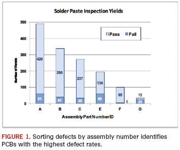
Ray Whittier of Vicor (vicr.com) has developed a simple yet highly effective recipe for mining the data his solder paste inspection system acquires. On the production floor, the machine is essentially a go/no-go gauge, indicating which prints can be passed on to pick-and-place and which must be removed from production. To make that decision, the machine collects a lot of data for each individual deposit, including solder paste height, area, volume, and X-Y position, and associates each data point with the package type, reference designator, pin number, date, time of day, etc. While the machine is dutifully executing its primary function of passing or failing prints, in the background it is generating a mountain of data that, when mined astutely, provides excellent diagnostic information.
Whittier’s first step is to download the database to an Excel spreadsheet for easy manipulation. Then he starts slicing and dicing:
- The first cut is by assembly number. This identifies the assemblies with the highest defect rates (Figure 1).
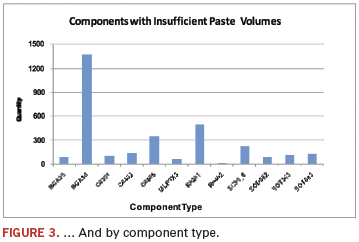
- The next cut looks at each of the top hitters individually. This view takes the data for each assembly number and carves them two ways:
a. By defect type (Figure 2).
b. By component type (Figure 3).
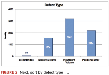
Sorting by defect and component type usually reveals a trend and points to the direction of the root cause. If a particular defect type is dominant, the root cause may be systemic. For example, if most failures are excessive solder volumes, he investigates the support tooling, looks for gasketing problems, and checks for undersized PWB pads. If the majority of failures are insufficients, he investigates paste release problems and checks for undersized stencil apertures that might drop area ratios (an aperture’s diameter divided by 4*foil thickness) below 0.66. If the defects are due to positional errors, he checks the printer’s program and the stencil positional accuracy.
Sorting by component type reveals the packages experiencing the most defects, and it’s no surprise the miniaturized components – 0.5 mm BGAs, 0201s and SOT883s – are the most problematic. To drill a little deeper into component-related defects, he looks at the defect modes and fallout rates of individual reference designators within the package types. Defects concentrated in a single location might be due to a tooling issue: a weak spot in the board support system, a component located near an edge clamp or irregularly formed stencil apertures. Drilling one step further to see the pin numbers where the defects are located identifies which apertures to check under the microscope. Alternatively, if defects are distributed across the board, he looks to the stencil, checking area ratios and measuring small apertures to make sure inadvertently undersized ones do not break the area ratio rule.
Download the data, filter it and sort it? It sounds almost too simple. Elegant is a better description, and successful. His process prints around 10,000 paste deposits in an area that’s roughly the size of a standard mail envelope at a 5.7∑ level. Impressive.
On highly miniaturized, densely packed PWBs, where one bad deposit causes an entire panel of 16 boards to get scrapped, the ability to quickly isolate and resolve the root causes of print problems is essential to an operation’s success. For Whittier, mining the data that his SPI system generates is one of the fastest ways to pinpoint the problem and get to its source. And while the method outlined here might not strike the mother lode every time, it always hits plenty of pay dirt.
Chrys Shea is founder of Shea Engineering Services (sheaengineering.com); chrys@sheaengineering.com.
ODMs offer unmatched product development expertise, while EMS firms have superior flexibility and service.
In a world of shrinking product development cycles and continual cost pressures, it is important to consider all costs in the outsourcing equation. Outsourcing options have continued to evolve, and the supplier’s choice of business model has both positive and negative cost implications. Here, we look at the advantages and tradeoffs between two of these business models: original design manufacturer (ODM) and electronics manufacturing services (EMS). Tailyn Communication Co. has had extensive experience with the differences between these models, as the company is both an ODM and EMS company that serves the industrial PC, wireless communications, point of sale and networking markets.
Outsourcing can provide a collaborative approach that leverages supplier expertise, purchasing power, manufacturing capability and logistics channels. However, achieving lowest total cost requires careful evaluation of project goals, outsourcing business models and supply base options.
Developing product around existing ODM technology may save time and cost in product development. In other cases, tapping an EMS provider with robust engineering skills may represent the best option.
Key Benefits of Each Model
The EMS business model taps shared engineering expertise, purchasing capability and manufacturing capacity. Its benefits can include:
- Access to a wider range of product development and engineering expertise than may be found internally at the OEM.
- Minimization of fixed costs associated with product manufacturing and reduction in working capital.
- Access to greater purchasing power.
- Access to robust project launch and design for manufacturability/testability (DfM/DfT) processes.
- Improvements in logistics efficiency.
- The offloading of operations such as repair depot not in line with core competencies.
The ODM model taps a supplier’s product development expertise. Advantages include:
- Speeding product development by incorporating ODM proprietary products and technology in new product development.
- Reducing tooling costs by using proprietary packaging or custom components.
- Access to application-specific expertise.
- Access to shared manufacturing capacity.
- Minimization of fixed costs and reduction in working capital.
Pros and Cons of the EMS Option
The traditional EMS model assumes the OEM owns the design and the contractor is primarily a manufacturing and logistics expert. The contractor may provide some support during the design phase, but traditionally this is related to DfM/DfT or procurement recommendations, rather than true conceptual design. That said, EMS providers typically have engineering expertise over a broad range of products and can act as extensions of their customers’ product development teams. This can be particularly attractive to companies with products requiring enhanced functionality, such as a medical product that needs to add communications capability.
The model leverages economies of scale in production resources. Customers have some flexibility in scheduling and specifying quality requirements and/or other preferences. From an inventory standpoint, the customer defines the approved vendor list (AVL) and may also set requirements for finished goods kanban quantity.
Non-recurring engineering (NRE) and tooling costs are typically charged at the beginning of the project, but the customer then owns tooling and documentation.
One of the biggest advantages of the EMS model is that its focus is service. Most EMS providers have the capability to support all phases of the product lifecycle, and in smaller and mid-size EMS providers, service and flexibility are often points of differentiation and value.
Finally, while changing EMS providers is not without cost, since the OEM owns its design and tooling, switching is always an option.
Pros and Cons of the ODM Option
While OEMs do leverage an ODM’s manufacturing resources, the largest part of the economies-of-scale savings is in product design and tooling. Typically in this model, OEMs are tapping the ODM’s proprietary technology, core parts of product design or packaging, and application-specific engineering expertise.
Understanding project goals and long-term strategy are critical in this type of relationship because the OEM and ODM can become permanent partners in shared product designs. This is because often the customer is simply licensing technology or product elements and using tooling owned by the ODM.
For example, sourcing to an EMS provider normally permits greater choice in facility locations. If the current EMS provider doesn’t have facilities in the desired build site region, it isn’t difficult to find an EMS provider with similar processes and equipment who does. Comparatively, changing ODMs may involve redesign and retooling.
Service and flexibility may also suffer. ODMs differentiate themselves by technology, engineering expertise and application-specific product lines. As a result, they aren’t typically interested in interrupting production with high mix products. Nor are they as open to customer-defined AVLs or finished goods kanbans.
If high mix or variable demand is likely to be an issue, it is important to understand the ODM’s track record in supporting high mix or variable demand projects. Talking to references with projects of similar size and complexity is one way to sanity-check this area of the business model.
Material leverage may be a strength for an ODM, since it may be a high user of application-specific components that other companies purchase in lower quantities. In those cases, restocking privileges may be more liberal and material liability may be reduced, since application-specific focus translates to higher levels of material commonality.
Software development is an area that should be watched closely. In some cases, the software platform is owned by the ODM. It is important to understand whether software is licensed or owned by the customer. One option that can provide enhanced flexibility in this area is hiring a third-party software developer. The positive is that the work is still outsourced. The negative is that it adds complexity and could create a longer learning curve. It can also make identifying problems a little more difficult, since if there are issues with the design, the two vendors may be blaming each other.
Availability of application-specific functional test equipment may be another advantage. Typically, an EMS provider expects this equipment to be consigned. However, an ODM may keep a much broader complement of equipment in-house to support its core technologies.
The biggest advantage is reduction in time-to-market. Being able to design a product around an established ODM platform can take months off the design cycle. Learning curve is minimized; components may already be in the pipeline, and packaging may already be tooled.
How do these benefits and tradeoffs translate in actual projects? These two case studies illustrate how each model supported each customer’s needs.
EMS case study. An industrial equipment firm with strong internal product development expertise wanted to improve its overall manufacturing efficiency by tapping the resources of an EMS provider.
The company had strong internal conceptual engineering resources, but wanted its EMS provider to handle DfM/DfT analysis and bill of materials (BoM) development. It wanted a unique product rather than one using another company’s proprietary technology.
Tailyn worked as an extension of their engineering team during the product development process. DfM/DfT recommendations included adjustments to PCB layout to maximize return on PCB size and address potential manufacturing quality issues in the SMT process. The original BoM was analyzed in terms of best supplier choices for price, quality and delivery performance, and second sources were added wherever possible.
The result of early contractor involvement was that one to two PCB design spins were eliminated, and both quality and supply chain flexibility were enhanced. Leveraging the EMS business model enabled the customer to do what it did best: design innovative new products.
ODM case study. A company with some internal design capability had an aging product platform. When sales started to drop, it was left with the choice of maintaining the existing platform and losing market share, or teaming with an ODM to rapidly develop a new platform.
It opted to team with Tailyn in a joint design effort because it would be able to incorporate the ODM’s technology in its new platform and launch new products faster than would have been possible with an internal new product development effort. It also freed its engineering team to work on other projects. In this case, the customer blended its expertise in product field performance knowledge and market intelligence with the ODM’s expertise in basic hardware architecture and software design.
The combined result was a new generation of product one year ahead of its competitors and the ability to stay price competitive on existing products.
The hybrid model. As indicated, it is possible to utilize a company that is both an ODM and an EMS provider. That is a situation where customers have more flexibility, since the benefits of both models are available.
However, even in a hybrid situation, it is important to understand that there are tradeoffs in each model. The highest level of product development expertise is found in the ODM model. The greatest degree of flexibility and service is likely to be found in the EMS model.
In making a final choice, alignment of expertise with project requirements, track record on similar projects and overall trustworthiness need to be carefully evaluated. A strong relationship is particularly important in a joint development or product incorporating shared design.
Key Questions to Ask When Considering Options
There are a number of critical questions when evaluating an ODM vs. EMS option:
- What is the desired product lifecycle length?
- What are internal core technology competencies and what technology expertise needs to be acquired in the outsourcing effort?
- What are the likely demand patterns?
- Are synergies on materials available from an ODM that would not be present in an EMS relationship?
- Who owns the tooling?
- Is the software licensed from the ODM or owned by the customer?
- Is there a local content requirement that would make one choice more attractive?
- Does the supplier have a track record of doing projects of similar size and complexity?
- Is there a contract that clearly defines the disengagement process and product ownership rights?
Ed.: This article is adapted from a presentation made at Surface Mount Technology Association International, October 2010.
Bibliography
1. J. Chen, “ODM or EMS: Which Choice is Best for Your Project?” Surface Mount Technology Association International Proceedings, October 2010.
Jim Chen is vice president sales division I at Tailyn Communication (tailyn.com.tw); jimchen@tailyn.com.tw.
Parameters that influence positional accuracy are studied on a number of laser-formed stencils.
For each method used to manufacture stencils, the important parameters are the quality of the equipment, the control over the process to fabricate the stencil, the quality and behavior of the metal during manufacture, the temperature differences during the various processes, and the varying tension on the materials in the different process steps.
The machine used to cut the stencils consists of two systems: the laser and the moving mechanism. The laser must have a small and very stable beam. The size of the beam determines whether very small details can be cut faithfully. If the beam is not stable in size and the main power concentration moves around, the kerf will not be exactly as intended; circular apertures will not be round, and straight wall apertures will have wavy sides (Figure 1).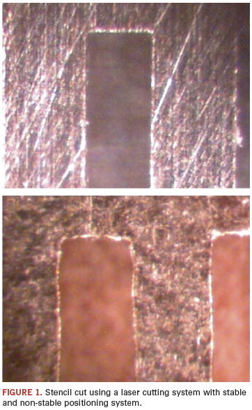
Most lasers produce a stream of high-power pulses to cut through the metal. Early lasers were pulsing at low frequencies, resulting in a scalloped cut when the metal was moved too quickly. Present day lasers employ a much higher pulse frequency, permitting faster cutting speed without resulting in a scalloped cut line.
To verify that the laser beam is stable and produces constant power, close examination of the aperture size, shape and wall is required. With a 40 to 100x microscope, it is easy to see whether the walls of an aperture are properly formed.
Various movement system designs exist. Early systems had a stationary laser beam, while the table holding the metal sheet or stencil frame moved in the X and Y axes. In some later systems, the beam moves in X axis and the table in the Y axis. The next step is to hold the metal stationary and move only the beam in the X and Y axes.
The reduction in mass to be moved makes it easier to increase cutting speed without sacrificing the ability to faithfully reproduce the detailed shapes of the stencil apertures.
In each design it is important that X and Y axes move perpendicularly to each other and that both move in a perfectly straight line (Figure 1). The movement system has to be perfectly calibrated to ensure control over the amount of movement to within a few micrometers. Most laser systems advertise location precision of 5 to 10 µm over a given distance.
Metals. The metal used for laser cutting has typically been stainless steel, type 302 or type 304, produced in a rolling mill. The resulting sheets are very uniform in thickness, but the specified thickness can typically vary by about 12 µm. To improve paste release, a number of post-processes have been tried: for example, electropolishing or chem-polishing, but not always resulting in improvements.
Other metals being introduced include nickel sheets and very fine grain stainless steels. The latter ones in particular have demonstrated significant improvements in the printing process.1
Electroforming. Stencils fabricated using the electroforming (EF) process consist of pure nickel. The EF process starts with a film that represents the aperture pattern to be manufactured. Making the film introduces additional process steps with their inherent possibility of errors, as film material is temperature- and moisture-sensitive. The film image is transferred in a photo process to a mandrel on which a metal layer is grown in an electrochemical process. To get a uniform thickness stencil requires that the chemical actions in the bath are exactly the same over the full area of the stencil. This can be difficult, especially when the aperture density varies greatly. Also, the growth of the metal immediately around an aperture can be faster, resulting in a small ridge or “dam” around the aperture. This dam has been used as a seal between the stencil and pad on the board. However, if this dam is not exactly aligned with the pad or it gets damaged, paste can leak through, which may result in solder balls.
The process also has to be well controlled so that it can be stopped at the proper moment when the sheet has grown to the desired thickness. After that it must be “peeled” off the mandrel without damaging the sheet, and then mounted in a frame.
Tension. When sheets are laser cut, they are typically clamped and tensioned in one direction, or they are cut already mounted in a frame.
If the sheets are mounted in the frame after cutting, the tension in both X and Y directions will often differ from the tension during cutting. The same, but more so, is true for stencils made with the electroforming process.
A stainless steel 125 µm (0.005") stencil manufactured without any stress on the metal and then placed in a frame exerting a stress of 35 Newton/cm (common mesh tension) sees a strain (percentage change in length) of 0.0131%. For a stencil image (or panel image) where apertures are 0.5 m (20") apart, this can cause an error of up to 65 µm (0.0025").
Temperature. Most stencil manufacturers produce stencils in air-conditioned rooms where the temperature is about 20ºC. In small, un-air-conditioned rooms, the temperature can easily vary by 5ºC or more. Similar variations can exist at the location where the stencils are used.
The coefficients of thermal expansion are approximately 17 ppm/ºC for steel and 13 ppm/ºC for nickel. This number indicates the expansion or contraction of the metal in microns per meter for each ºC. For a stencil image (or panel image) where apertures are 0.5 m (20") apart, and the temperature difference between fabricating the stencil and using the stencil is 5ºC, the change in dimension in a steel stencil can be 42 µm (0.0017"). For a nickel stencil it would be about 32 µm (0.0013").
While laser cutting, the hot beam can cause a local temperature rise in the metal that can lead to discoloration (innocent) or even deformation through local expansion of the metal (troublesome). Proper beam control and metal cooling (airflow or liquid cooling) can minimize this problem.
Impacts on Use
For newer components, such as CSPs and very small passive components, the space between pads on the board can be less than 200 µm (0.008").
To prevent significant errors as described above, employ the best stencil manufacturing equipment and practices possible. That also means working in a controlled environment, both at the stencil manufacturer and user locations. To prevent errors due to possible tension differences, it is desirable to cut the stencil while mounted in the frame. In short, as a stencil user it is becoming necessary to know what equipment and what process is used and what checks are made by the stencil manufacturer.
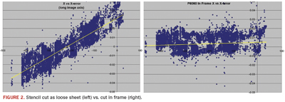
Figure 2 shows an example of one stencil cut from a sheet and then mounted, and another cut in the frame on the same laser. A definite change in the error trend can be observed.
Stencil verification. The simplest way to determine stencil precision is to scan it and determine the location and size of each aperture. Available systems can perform such tests to accuracies of +/-5 µm (0.002") within a few minutes. A computer program can determine the centroid and size of each of the scanned apertures and compare those to the original design. The resulting data can be used for an easy go/no-go determination, or to perform statistical analysis.
The new scanned laser-cut stencil may have remaining loose particulate in some of the apertures. This interferes with the centroid and area calculation, but can easily be recognized and therefore excluded from the results (Figure 3).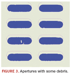
A large stencil (about 460 x 300 mm) with about 21,000 apertures was selected for these tests. Stencils were measured using a well-calibrated scanner (ScanCheck) with a resolution of 6,000 pixels per inch (12,000 with interpolation). The resulting numbers were then compared to the cutting data and errors beyond a given specification presented. All data collected can be exported for further analysis, as is done here. For this analysis, only the location errors along the long stencil axis are used.
Comparative Measurements
For comparison purposes, a number of stencils were produced using different methods, machines and processes. These stencils were produced using commonly available laser-cutting and electroforming production methods. Four different laser system brands, for a total of seven different types of machines, were selected. Of these stencils, five were produced both as sheets and in a frame and two cut in a frame, for a total of 13 laser cut stencils and one electroformed stencil.
The stencils were produced in several different commercial facilities, and environmental conditions were not recorded; therefore, a temperature effect cannot be established separately from the machine accuracy and tension effects.
A specification of +/-10 µm was used, and for each stencil, the extent and distribution of the location errors were calculated. This aforementioned specification limit is a commonly used value for allowable tolerance by many large EMS companies. The value of Cp indicates how often this distribution of the data fits between the specification limits (Figure 4). For these very large and complicated stencils, only one showed a Cp value greater than 1 (Figure 5). In the individual graphs, the short green bars represent the three sigma limits. At those points the error rate is 2,750 ppm. Of course, Six Sigma would be more desirable, where the error rate would be only 0.002 ppm.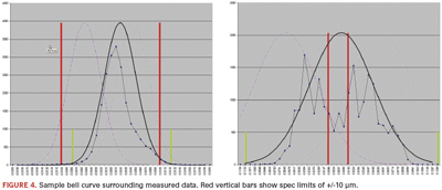
As the stencil can be shifted and aligned to the board in the printer, the Cpk value, which uses the worst half of the distribution and the deviation of the mean from the center of the specification, has not been determined.
Results. The resulting Cp values for the whole group of stencils are shown in Figure 5. Yellow bars show the Cp values for stencils cut as loose sheets, and blue bars show the range for stencils cut in the frame. For the measured apertures, the error range (brown bars) varies from 35 to 185 µm (0.0014"to 0.0073").
The data show a noticeable grouping based on the chosen manufacturing techniques. In general, stencils cut in a mounted frame show significantly higher aperture positional accuracy than stencils cut as loose sheets and subsequently mounted into a frame. 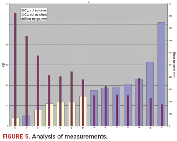
Figure 6 shows the distribution of the data for a stencil cut in the frame and as a sheet using the same laser. The noticeable change in the spread of the data shows the result of the change in tension while cutting the stencil versus the tension after the stencil has been mounted in a frame.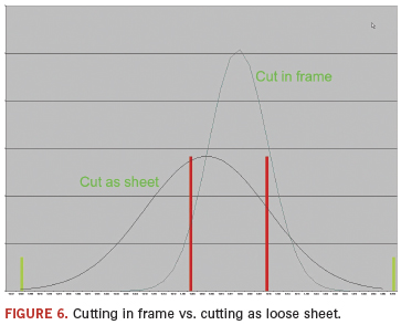
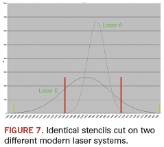
Another factor for the change in positional accuracy is the choice of laser cutting system. In general, we can observe that most newer systems (fewer than three years old) provide a higher positional accuracy compared to the older systems (three to 15 years old). However, even among new laser systems we can observe a significant difference in aperture positioning accuracy between different laser systems. These differences are probably related to system architecture and calibration methods used. Figure 7 shows the change in the spread of the data for two stencils cut in the frame on two different laser systems.
Conclusion
When printing on a board with components that have large pads and large spaces between pads, a significant alignment error between the stencil apertures and board pads may not cause serious issues. It is like a form of overprinting, and many solders, in their molten state, will wick back onto the pad.
However, many of today’s boards have tiny parts with very small and closely spaced pads where such errors might cause bridging. Also, Pb-free solder does not spread as well as Pb-bearing solder. Therefore, the size of the errors encountered in several of these stencil samples will lead to unacceptable levels of production errors.
For a stencil with optimum aperture positioning accuracy, we can conclude that laser cutting shows better results than photo-based processes; stencils cut in a frame show very little distortion, and stencils cut on modern lasers show significantly better positioning accuracy.
Note that additional printing errors can come from, among others, low mesh tension, inadequate squeegee pressure or insufficient board support.
Acknowledgments
The authors thank Florian Roick of LPKF Laser & Electronics, Mike Scimeca of FCT Assembly and Frank Kurisu of Solder Mask Inc. for their kind contributions to this article.
References
1. Robert F. Dervaes, Jeff Poulos and Scott Williams, “Conquering SMT Stencil Printing Challenges with Today’s Miniature Components,” Global SMT & Packaging, April 2009.
Ed. This article was first published at the SMTA Pan Pac Conference in January 2011 and is republished here with permission of the authors.
Ahne Oosterhof is founder of Oosterhof Consulting; ahne@oosterhof.com. Stephan Schmidt is general manager of LPKF Laser & Electronics (www.lpkfusa.com); sschmidt@lpkfusa.com.

Periodic pot emptying and cleaning, plus nitrogen use, helps reduce dross formation.
In the selective soldering process, dross can be detrimental. Dross (the term as used here encompasses all surface contamination) is created in conjunction with the presence of oxygen in two different areas of the process, and by separate means. Each must be dealt with differently to prevent problems.
Conventional dross, as most people know it, is created when the solder basically tumbles back into the solder pot from the nozzle. As the solder flows back into the pot, down the drop area from the nozzle tip, it mixes with the atmosphere and oxidizes to create a chowder-like substance known as dross. This dross is usually a combination of oxidized solder alloy and spent flux. In Pb-based alloys, dross typically floats on top of the solder in the tank and doesn’t cause any particular problems. The high density of the Pb-based alloy (e.g., Sn63) ensures it remains on top and won’t be drawn down into the pump, clogging the nozzle, or comingling with fresh solder being deposited on the board.
A second type of dross is created by the spindle of the impeller pump driveshaft as it rotates in molten solder. This is actually the product of the metal-to-metal contact (even though the solder is liquidous), the product of essentially a burnishing operation, a rubbing and scrubbing of the metals. The rotating shaft creates an interaction with the molten solder and generates a residue, typically a SnPb oxide or a tin oxide, and it evidences itself in the form of a fine black powder that floats on top of the solder and around the drive shaft.
This black powder-like material can be detrimental to lead or Pb-free soldering because it can be drawn into the pump. As the spindle of the impeller rotates, depending on the volume of this black residue, the rotation can set up a vortex, or whirlpool, during which time the material can be sucked into the impeller area. It then gets into the pumped solder as it is being delivered into the nozzle. It tends to collect, and therefore can contribute to the clogging of nozzles, especially small ones. The smaller the nozzle, the more susceptible it is to clogging with this material. Moreover, that black particulate matter, present in the solder flow, can also deposit itself onto the board, even into the solder fillet itself. This is a concern not only in selective soldering, but also in wave soldering, and in both instances is a product of the pumping process.
To mitigate these issues, solder pot and pumping assembly can be enclosed and the area above the solder and below the cover filled with superheated nitrogen. The nitrogen is permitted to escape only from the area surrounding the nozzle. Doing so inerts the entire solder delivery process, and the return area of the solder to the solder pot, and can sharply reduce conventional dross formation. Black powder dross can be mitigated with nitrogen or the use of protective graphite sleeves around the pump shaft, which act as a barrier, protecting the rotational effects of the pump impeller from interacting with molten solder.
When using Pb-free alloys, dross can be a little more problematic, due in part to the lower density of the Pb-free alloy. For instance, a wrench will float on top of a solder pot full of Sn63, but it will quickly sink to the bottom of a pot of Pb-free alloy. Contamination that typically floats on a solder pot filled with Pb-based alloy, and is therefore easy to remove, may not float on top of a pot of Pb-free alloy, and can drop to the bottom and comingle with the pumped solder. It is imperative to ensure that the surface of the solder is clean daily, and pull the pump assembly and clean the bottom of the solder pot at least four times as often as one would with a pot of Sn63.
It’s easy to test the effectiveness of this nitrogen-inerting approach. We perform a fairly simple empirical test to confirm nitrogen purity and performance and its effects on the wave. We simply tin the nozzle, set the appropriate level of nitrogen purity and flow, and run the flowing solder at full production readiness for a 15-min. interval, during which time we observe the operation closely. We’re not soldering a board at this time, but actually running in free air, with the nitrogen surrounding the nozzle. If no discoloration of the flowing solder is observed, we know that the volume and purity setting of the nitrogen is sufficient to protect that nozzle and mitigate the dross.
Typically, at the end of an 8-hr. shift, one may expect to find about a tablespoon of residue floating on top of the solder pot. It’s largely spent flux mixed with a little dross, and that’s normal and also usually easy to remove. Dross in the bottom of the pot, particularly when using Pb-free solders, can be removed only by emptying the pot. The interval can be determined by the user. In the beginning, more often is better; if, upon inspection of the emptied pot, it can be prudently determined that the frequency is too great (little or no residue), then that PM interval can be increased, provided of course that throughput volume remains mostly static.
Alan Cable is president of A.C.E. Production Technologies (ace-protech.com); acable@ace-protech.com.

Press Releases
- Green Circuits Announces Strategic Partnership with Metatron Private Equity
- Smartsol Technologies Mexico Strengthens its X-ray Division and Announces Strategic Partnership Expansion with Creative Electron
- Hanwha Semitech Americas Supports Regal Technology Partners with New SMT Line Installation
- AIM Hires Marcus Pee as Sales Engineer for Southeast Asia