

The patent circuit: from application to enforcement.
On the surface, a patent is a fairly simple concept. It protects an invention. However, just as designing, engineering and manufacturing a product is a complex process fraught with potential risks, a patent is much more than simply protection for an invention.
The concept behind the US patent system goes all the way back to the original US Constitution ratified in 1787. Even before there was a Bill of Rights and such American concepts as freedom of speech and due process, Congress had the power to “promote the progress of science and useful arts, by securing for limited times to authors and inventors the exclusive right to their respective writings and discoveries.” From that Constitutional authority, the US patent system was founded. A patent is a time-limited monopoly granted by the federal government to inventors. A patent encourages innovation by giving a patent owner exclusive rights to his or her invention.
A US patent always names an inventor or inventors. If the patent was developed by inventors working for a business or researchers working for a university or other institution, the patent is often assigned to the inventors’ employer. In such cases, a patent has both an inventor or inventors and an assignee.
A patent is an exclusionary right. It is the right to exclude others from using the patented invention without permission of the inventor or assignee. Title 35 of the United States Code (or “35 USC”) is the federal law that covers patents. Section 271 of 35 USC defines patent infringement as when a person or other entity “makes, uses, offers to sell, sells or imports” a product or service that uses the patented invention without the patent owner’s permission.
There are three types of patents: The most common is the Utility Patent that covers a product, device, process or composition of matter. There is also a Design Patent that covers the appearance of a product and not how the product operates, and there are Plant Patents that cover asexually reproduced vegetables, fruits, trees and other botanical species. The term of a Utility Patent is 20 years from the date of application.
The US Patent and Trademark Office (or USPTO or simply “Patent Office”) currently issues about 180,000 patents a year, about half to US residents. The USPTO is an agency of the US Department of Commerce and is headquartered in Alexandria, Virginia. The Patent Office is just one of a few self-funded federal agencies. The USPTO uses no tax dollars, but is funded entirely from the money it collects from application and maintenance fees.
What a patent is not. There is a common misconception about patents. Since patent infringement occurs if a patented invention is used without permission from the patent owner, many people assume that you therefore need a patent to “make, use, offer to sell, sell or import” a product that uses your own invention. Not true. A patent is not the right to use your own patented invention; it is only the right to exclude others from using your patented invention!
You only need permission to make, use, offer to sell, sell or import a product that uses someone else’s patented invention. In that case, your options are to buy the patent (patents are assets that can be bought and sold like inventory, real estate and securities), license the patent (have the patent owner agree to let you use the patent in exchange for a fee, usually a royalty based on unit or dollar sales of the product that uses the patent), or infringe the patent and risk a patent infringement lawsuit by the patent owner.
So, if no patent is required to practice your own invention, should you patent your latest technology?
To patent or not to patent. That is, indeed, the question! While a patent gives you the right to exclude others from making, using, offering to sell, selling or importing a product that embodies your patented invention, that exclusionary right comes with a condition: You must publish
your invention.
All patents are public documents. Before the Internet, the Patent Office operated patent libraries – the agency still does – in federal office buildings across the country, where anyone could view a patent. Today, of course, all US patents are available online. So a patent is essentially a bargain with the federal government. In exchange for the right to exclude others from making, using, offering to sell, selling or importing a product that uses your patented invention, you must disclose your invention to the public.
The reasoning behind this is that each invention in turn leads to the next invention. Public disclosure of inventions prevents another inventor from having to reinvent what has already been invented, but instead jump to that point in the technology and work forward from there. Among patent practitioners, patents are generally classified as a “fundamental” patent – one that represents a breakthrough technology like the telephone, airplane or transistor – and an “improvement” patent that takes an existing concept to the next level. And it looks like the system works, since the US continues to be the global leader in innovation, in no small measure a result of the US patent system.
Why not patent an invention? Under what circumstances might an inventor or business decide not to patent its latest new technology? The alternative to patenting an invention is to keep the technology under wraps as what is called a “trade secret.”
Like everything else in business, technology and law, there are benefits and drawbacks to patenting your invention or keeping it as a trade secret. While you lose the protection afforded by a patent, you gain the advantage that you do not have to publish your invention if you decide to keep it as a trade secret. If you do not file for a patent, you can simply keep your invention as your own secret, proprietary technology. However, the process of keeping a trade secret “secret” is by no means simple.
As long as none of your competitors reinvents or reverse-engineers your new technology, you can keep and practice your trade secret for years … maybe forever. The Coca-Cola Co. made the critical decision over 100 years ago not to patent the formula for its soft drink. Had the company patented the formula, once the patent expired, any competitor would have been free to duplicate it and produce an identical beverage.
However, going the trade secret route runs the risk that a competitor either reinvents your invention or reverse-engineers it. At that point, your competitor is free to make, use, offer to sell or sell products or services that use your invention because there is no patent on it, and there is nothing you can do about it.
As a result, if you decide to keep your newest mousetrap a trade secret, you need to put into effect safeguards that will, in fact, keep it secret. The new technology can only be revealed to a small, select group of employees on a strictly need-to-know basis, and all documentation must be kept under lock and key. The Coca-Cola formula is reputedly kept in a vault in an Atlanta bank and is known only to a key group of senior, trusted employees. In fact, Coca Cola legend has it that the company purposely buys ingredients that do not go into the soft drink just to throw off their competitors as to what is actually in the formula!
What should be patented, and what should not? While every new technology has to be considered on a case-by-case basis, a general rule to start with is that most products should be patented, while a process may be a candidate for trade secret. The logic is that a product can be purchased by a competitor who can disassemble, study and examine it, then reverse-engineer it to duplicate what you did to produce a very similar or identical product.
A process, however, that is not seen by the public and that does not leave a fingerprint is a candidate for trade secret. If what you do in your plant, laboratory or other facility to produce a product or service is not seen by the public, and it would be very difficult (or, better yet, impossible) for a competitor to reverse-engineer your secret process, it may be the better option to keep your process as a trade secret. What the ingredients are in the Coca-Cola formula, how they are blended, and under what circumstances must be very difficult to reverse-engineer based on the fact that no one has been able to do it over the last 100 years.
The other factor that cuts across all of this is the life expectancy of the new product. Your patent will only give you protection for 20 years from the date of filing of your patent application. If the life of the product that uses your patented invention is likely to be less than 20 years – as it is today with many high-tech products – that means that by the time your patent expires and competitors are free to copy it, it will be obsolete anyway. We do not know if John Pemberton, the inventor of Coco-Cola, knew that his drink would capture the hearts, minds and taste buds of America and would endure for over 100 years, but he obviously made the right decision to not patent the formula. Had Pemberton filed for a patent when he developed the Coca-Cola formula in 1886, the patent would have expired over 100 years ago!
In short, if it is likely that a competitor could re-invent or reverse-engineer your invention, you are better off patenting it. If it is unlikely that a competitor could re-invent or reverse-engineer it, you might consider keeping it a trade secret. And that is a tough call to make!
Receiving a patent. The requirements for an invention to receive a patent are that it be novel (that is, new, and something that has not been done before), non-obvious (it is not something that another person could have easily figured out or come up with on his or her own) and useful (it must have a practical application).
Most inventors engage a patent attorney to assist with the patent application process. It currently takes about three years to receive a patent, and the entire process will run several thousand dollars in Patent Office and patent attorney fees.
Fighting infringement. Let’s say you file for and receive a patent, and you come across a product or service that appears to infringe your patent. First, it is entirely possible that the product or service does exactly what your patented product or service does, but does so in a different manner, and so does not infringe your patent. For example, a gasoline engine looks like and performs the same function as a diesel engine, but the technologies are totally dissimilar.
In order for a product or service to infringe your patent, it must duplicate all the elements in at least one claim in your patent. The term patent professionals use is that the product or service must “read on” at least one claim in the patent.
Should you believe that a product or service is infringing your patent, the remedy available is to file a patent infringement lawsuit in US District Court. If your case goes to trial and you win, the court will award “reasonable royalties”: what it believes the infringer would have paid in royalties had the infringer licensed your patent in the first place.
However, like most civil litigation, most patent infringement lawsuits do not go to trial but are settled out of court. Should the infringer agree to a settlement, the amount will likely be computed along the same lines – what would the royalty have been had the infringer licensed the patent? Your settlement will likely also include a license with the infringer to cover future use of your patent (if the patent has not expired).
Compensation of reasonable royalties for the infringement of a patent is predicated on the basis that the infringement was unintentional. That is, the infringer accidentally reinvented your patented invention, and did not know it was infringing your patent. However, should you be able to prove willful infringement – the infringer was aware of your patent but went ahead and decided to make, use, offer to sell, sell or import a product that used your patented invention anyway – the court may punish the infringer by awarding additional damages. The court could award as high as triple (or “treble” in legalspeak) damages. However, proving willful infringement is very difficult, and if the defendant settles out-of-court, it is highly unlikely that it will admit to willful infringement.
A select group of patent owners that meets very specific requirements may be able to receive “injunctive relief,” an injunction from the court ordering the infringer to cease making, using, offering to sell, selling or importing the infringing product. There are a few exceptions, but injunctive relief is not available to most patent owners that do not practice their patents. Such a patent owner is known as an NPE (“non-practicing entity”). However, in limited circumstances, a patent owner that practices its patent (a “market participant”) may be granted injunctive relief, if it also meets other critieria.
The question the patent owner facing infringement must ask is: Do I want justice, or do I want compensation? If your patent is being infringed by a direct competitor that is stealing sales and profits that rightfully belong to your company, then it may be justice in the form of a court injunction. However, if the infringer is a much larger company, or it operates in a different industry, and you can prove infringement and reach a settlement with the infringer, compensation for the use of your patent could turn out to be a very nice revenue stream!
Since patent infringement is not a crime, there are no “patent police.” It is the job of the patent owner to enforce their or its patent. Filing a patent infringement lawsuit can be very expensive, running from a few hundred thousand dollars to several million dollars. It only makes sense to pursue an infringer that is generating millions of dollars a year in sales from the product that infringes your patent, or there will not be a large enough return – from an award from a trial or from an out-of-court settlement – to cover litigation expenses.
For the patent owner that does not have the capital to spend on a lawsuit, there are a few law firms that will work on a contingency basis, taking part or most of their fees from any awards or settlements they secure on behalf of the patent owner. There are also patent enforcement firms that specialize in managing and financing patent enforcement campaigns on behalf of patent owners on a 100% contingency basis. Under the patent enforcement firm business model, the patent owner pays nothing, and the patent enforcement firm bears all costs, manages the entire patent enforcement campaign, engages and supervises a law firm to try the lawsuit, and offers several additional services.
Most businesses do a pretty good job of protecting their traditional assets – inventory, equipment, real estate and cash – but these are all assets that can be easily replaced. In today’s intensely competitive flat world, a company’s intellectual assets are far more valuable – and far more difficult to replace – than its balance sheet assets. Every business needs to have a plan to protect its innovations, technologies and know-how, either by patenting it or securing it as a trade secret.
Kathlene Ingham is director of licensing at General Patent Corp. (generalpatent.com); kingham@generalpatent.com.
How to configure systems and account for error sources.
Electrostatic discharge or a release of static charge can damage sensitive electronic components, resulting in failures, reduced reliability and increased rework costs, or latent component failures in equipment in the field. That potential for damage makes the ability to characterize charge accurately extremely important for electronics manufacturers.
Charge, as we all learned in introductory physics, is the time integral of current.  Eq. 1
Eq. 1
Charge is often measured on a quantity of particles, on a surface, or on a component such as a capacitor. Sometimes, charge is measured on a continuous basis, such as when using the coulombmeter to measure very low current. An electrometer makes an ideal coulombmeter because it has very low input offset current and high input resistance. The coulombmeter function of the electrometer measures charge by integrating the input current. An integrating capacitor is used in the feedback loop of the input stage (Figure 1).
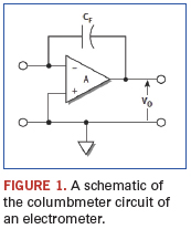
Electrometers are ideal for charge measurements, because their low offset current won’t alter the transferred charge during short time intervals, and their high input resistance won’t allow the charge to bleed away. Electrometers use a feedback circuit to measure charge, as shown here. The input capacitance of this configuration is ACF. Therefore, large effective values of input capacitance can be obtained using reasonably sized capacitors for CF.
As accurate as electrometers are, a variety of error sources can degrade charge measurement integrity if not taken into account. These error sources include input offset current, voltage burden, generated currents, and low source impedance.
Input offset current. Input offset currents are background currents that are present in the measuring instrument when no signal current is applied to the instrument. With an electrometer, the input offset current is very low. However, at low charge levels, even this small current may be a significant error factor. Over long periods, the instrument will integrate the offset current, which will be seen as a long-term drift in the charge measurement. Typical offset current is four femto-amps, which will cause a change in the charge measurement of four femto-coulombs per second. If the offset current is known, it’s possible to compensate for this error simply by subtracting the charge drift due to offset current from the actual reading. However, determining the offset current of the entire system is likely to be significantly more complicated.
Voltage burden. The voltage burden of an ammeter is the voltage drop across the input terminals. The voltage burden of a feedback coulombmeter is generally quite low (less than 100 microvolts). However, if the instantaneous peak current is more than 10 micro-amps, the voltage burden can exceed this level momentarily. In an overload condition, the voltage burden can reach many volts, depending on the input value. If the source voltage is at least 10 mV, the typical electrometer in the coulombs mode will integrate the current accurately. However, if the source voltage is much lower, the voltage burden may become a problem, and the input stage noise will be amplified so much that making accurate measurements is impossible.
Generated currents. Generated currents from the input cable or induced currents due to insufficient shielding can cause errors in charge measurements, especially with charge levels of 100 pC or less. To minimize generated currents, always use low noise cable and electrostatically shield all connections and the DUT.
Source impedance. The magnitude of the source impedance can affect the noise performance of the feedback coulombmeter. Figure 2 illustrates a generalized feedback circuit connected to a source impedance. In a coulombmeter, the feedback impedance is a capacitor. The noise gain of the coulombmeter can be calculated from this equation:
Output noise = Input noise × (1 + ZF/ZS) Eq. 2
where: ZS is the source impedance
ZF is the feedback impedance of the coulombmeter
Input noise is the noise of the input stage of the electrometer
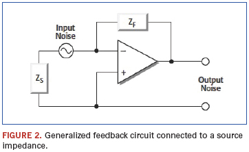
In general, as ZF becomes larger, the noise gain increases. The documentation or specifications for the particular electrometer being used will generally provide the value of its feedback impedance.
Other Charge Measurement Considerations
Unlike a voltage measurement, a charge measurement is a destructive process. That is, the process of making the measurement may remove the charge stored in the device under test. When measuring the charge on a device such as a capacitor, it’s important to disable the zero check of the electrometer first, and then connect the capacitor to the high impedance input terminal. Zero check is a process where the input amplifier of the electrometer is reconfigured to shunt the input signal to low. Otherwise, some of the charge will be lost through the zero check impedance and won’t be measured by the electrometer. That’s because when zero check is enabled, the input resistance of the electrometer is about 10 MΩ. Opening the zero check switch produces a sudden change in charge reading known as “zero hop.” To eliminate the effects of zero hop, take a reading just after the zero check is disabled, then subtract this value from all subsequent readings. An easy way to do this is to enable the REL function after zero check is disabled, which nulls out the charge reading caused by the hop.
The charge measurement range of most electrometers can be extended through the use of the external feedback mode, which allows use of an external device as the electrometer’s feedback element. Placing the electrometer in the volts mode and then enabling external feedback switches the feedback circuit from an internal network to a feedback circuit connected to the preamp output.
To extend the coulombs ranges, an external capacitor is used as the feedback element. An external feedback capacitor is placed between the preamp output terminal and the HI input terminal of the electrometer (Figure 3). To prevent electrostatic interference, the capacitor is placed in a shielded test fixture.
When in external feedback mode, the electrometer will display the voltage across the feedback element. The unknown charge can be calculated from the following formula:
Q = CV Eq. 3
where: Q = charge (coulombs)
C = capacitance of the external feedback capacitor (F)
V = voltage on display of electrometer (V)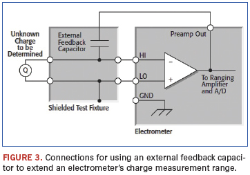
For example, using an external feedback capacitor of 10 mF and measuring 5V on the display of the electrometer, the calculated charge is 50 µC. The capacitance of the feedback element should be at least 10 pF to avoid errors due to stray capacitance and noise gain. To ensure low leakage current and low dielectric absorption, the feedback capacitor should be made of a suitable dielectric material such as polystyrene, polypropylene, or Teflon.
Several other elements of measurement “hygiene” are critical to making good charge measurements with electrometers, including making proper connections, minimizing electrostatic interference, and minimizing the impact of environmental factors.
Making connections. To avoid measurement errors, it’s critical to make proper connections from the electrometer to the device under test. Always connect the high-resistance terminal of the meter to the highest resistance point of the circuit under test.
Electrostatic interference and shielding. Electrostatic coupling or interference occurs when an electrically charged object approaches the input circuit under test. At low impedance levels, the effects of the interference aren’t noticeable because the charge dissipates rapidly. However, high-resistance materials don’t allow the charge to decay quickly, which may result in unstable measurements. The erroneous readings may be due to either DC or AC electrostatic fields, so electrostatic shielding will help minimize the effects of these fields.
DC fields can produce noisy readings or undetected errors. These fields can be detected when movement near a test setup (such as the movement of the person operating the instrument or others in the immediate vicinity) causes fluctuations on the electrometer’s display. To perform a quick check for interference, place a piece of charged plastic, such as a comb, near the circuit. A large change in the meter reading indicates insufficient shielding.
AC fields can be equally troublesome. These are caused most often by power lines and RF fields. If the AC voltage at the input is large, part of this signal is rectified, producing an error in the DC signal being measured. This can be checked by observing the analog output of the electrometer with an oscilloscope. A clipped waveform indicates a need to improve electrostatic shielding.
AC electrostatic coupling occurs when an electrostatic voltage source in the vicinity of a conductor, such as a cable or trace on a printed circuit board, generates a current proportional to the rate of change of the voltage and of the coupling capacitance. This current can be calculated with the following equation:
i = C dV/dt + V dC/dt Eq. 4
For example, two conductors, each with 1cm2 area and spaced 1cm apart by air, will have almost 0.1 pF of capacitance. With a voltage difference of 100V between the two conductors and a vibration causing a change of capacitance of 0.01 pF/sec. (a 10% fluctuation between them), a current of 1pA AC will be generated.
To reduce the effects of the fields, a shield can be built to enclose the circuit being measured. The easiest type of shield to make is a simple metal box or meshed screen that encloses the test circuit. Shielded boxes are also available commercially. Made from a conductive material, the shield is always connected to the low impedance input of the electrometer.
The cabling between the HI terminal of the meter and the device under test also requires shielding. Capacitive coupling between an electrostatic noise source and the signal conductors or cables can be greatly reduced by surrounding those conductors with a metal shield connected to LO. With this shield in place, the noise current generated by the electrostatic voltage source and the coupling capacitance flows through the shield to ground rather than through the signal conductors.
To summarize, follow these guidelines to minimize error currents due to electrostatic coupling:
- Keep all charged objects (including people) and conductors away from sensitive areas of the test circuit.
- Avoid movement and vibration near the test area.
- When measuring currents of less than 1 nano-amp, shield the device under test by surrounding it with a metal enclosure and connect the enclosure electrically to the test circuit common terminal.
Although the word “shielding” usually implies the use of a metallic enclosure to prevent electrostatic interference from affecting a high impedance circuit, guarding implies the use of an added low impedance conductor, maintained at the same potential as the high impedance circuit, which will intercept any interfering voltage or current. A guard doesn’t necessarily provide shielding.
Environmental factors. A stable test environment is essential for making accurate low level measurements of all types.
Temperature and temperature stability. Varying temperatures can affect low level measurements in several ways, including causing thermal expansion or contraction of insulators and producing noise currents. Also, a temperature rise can cause an increase in the input bias current of the meter. As a general rule, JFET gate leakage current doubles for every 10°C increase in temperature, but most electrometers are temperature compensated to minimize input current variations over a wide temperature range. To minimize errors due to temperature variations, operate the entire charge measurement system in a thermally stable environment. Keep sensitive instruments away from hot locations (such as the top of a rack) and allow the complete system to achieve thermal stability before making measurements. Use the instrument’s zero or suppress feature to null offsets once the system has achieved thermal stability. Repeat the zeroing process whenever the ambient temperature changes. To ensure optimum accuracy, zero the instrument on the same range as that used for the measurement.
Humidity. Excess humidity can reduce insulation resistance on PC boards and in test connection insulators. A reduction in insulation resistance can, of course, have a serious effect on high impedance measurements. In addition, humidity or moisture can combine with any contaminants present to create electrochemical effects that can produce offset currents.
To minimize effects of moisture, reduce humidity in the environment (ideally <50%). Ensure all components and connectors in the test system are clean and free of contamination. When cleaning, use only pure solvents to dissolve oils and other contaminants; then rinse the cleaned area with fresh methanol or deionized water. Allow cleaned areas to dry for several hours before use.
Ionization interference. Current measurements made at very low levels (<100fA) may be affected by ionization interference from sources such as alpha particles. A single alpha particle generates a track from 30,000 to 70,000 positive and negative ions per cm, which may be polarized and moved about by ambient electric fields. Also, ions that strike a current-sensing node may generate a “charge hop” of about 10 fC per ion. There are several ways to minimize test system noise due to ionization interference. First, minimize the volume of air inside the shield around sensitive input nodes. Also, keep sensitive nodes away from high-intensity electric fields.
RFI. Interference from radio frequency sources can affect any sensitive electrometer measurement. This type of interference may be indicated by a sudden change in the reading for no apparent reason. A nonlinear device or junction in the input circuit can rectify the RF energy and cause significant errors. Sources of such RFI are nearby transmitters, contactors, solenoid valves, and even cellular telephones and portable two-way radios. Once the source is identified, the RF energy may be reduced or eliminated by shielding and adding snubber networks or filters at appropriate points.
Common Charge Measurement Applications
Charge measurements include applications such as measuring capacitance and static charge on objects. Charge measurement techniques can also be used to measure very low currents (less than 10 femto-amps, or fA).
The coulombs function of an electrometer can be used with a step voltage source to measure capacitance. This technique is especially useful for testing cables and connectors because it can measure capacitances ranging from <10pF to hundreds of nanofarads, or nF. The unknown capacitance is connected in a series with the electrometer input and the step voltage source. The calculation of the capacitance is based on this equation:![]() Eq. 5
Eq. 5
Figure 4 illustrates the basic configuration for measuring capacitance with an electrometer with a built-in voltage source. The instrument is used in the charge (or coulombs) mode, and its internal voltage source provides the step voltage. Just before the voltage source is turned on, the meter’s zero check should be disabled and the charge reading suppressed by using the REL function to zero the display. Then, the voltage source is turned on and the charge reading noted immediately. The capacitance is calculated from:![]() Eq. 6
Eq. 6
where: Q2 = final charge
Q1 = initial charge assumed to be zero
V2 = step voltage
V1 = initial voltage assumed to be zero
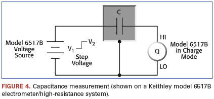
After the reading has been recorded, reset the voltage source to 0V to dissipate the charge from the device. Before handling the device, verify the capacitance has been discharged to a safe level. The unknown capacitance should be in a shielded test fixture. The shield is connected to the LO input terminal of the electrometer. The HI input terminal should be connected to the highest impedance terminal of the unknown capacitance. For example, when measuring capacitance of a length of coaxial cable, connect the HI terminal of the electrometer to the center conductor of the cable, allowing the cable shield to minimize electrostatic interference to the measurement.
If the rate of charge is too great, the resulting measurement will be in error because the input stage becomes temporarily saturated. To limit the rate of charge transfer at the input of the electrometer, add a resistor in a series between the voltage source and the capacitance. This is especially true for capacitance values greater than 1 nF. A typical series resistor would be 10 kΩ to 1 MΩ.
As mentioned, a Faraday cup is useful for measuring static charge on objects. This is useful because insulators permit only a slight motion of electrons, which allows electrostatic charges to build up on a material and create hazards. The problem generally is not the static charge itself on the object, but rather the spark generated when the object discharges. Therefore, in order to understand and control these problems, it’s necessary to measure the static electricity on an object. This can be done by placing the object in a Faraday cup and measuring the charge with an electrometer. The Faraday cup method can be used to measure the charge on a wide range of substances and objects, such as plastics, films, liquids, gases, and electronic components.
A Faraday cup (sometimes called a Faraday cage or icepail) is an enclosure made of sheet metal or conductive mesh (Figure 5). The electric field within a closed, empty conductor is zero, so the cup shields the object placed inside it from any atmospheric or stray electric fields. This enables the accurate measurement of the charge.
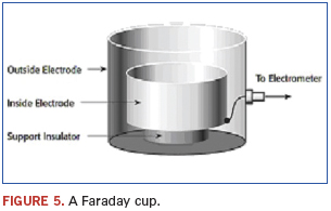
A Faraday cup consists of two electrodes, one inside the other, separated by an insulator. The inside electrode is connected to the electrometer HI, and the outside electrode is connected to the electrometer LO. When a charged object is placed within the inside electrode, an induced charge will flow into the electrometer.
A Faraday cup can have virtually any dimensions, depending on the size and shape of the object to be tested. Cylindrical and spherical shapes are typically the most convenient choices; simple containers such as coffee or paint cans are often used. The electrodes can be made of any conductive material. The support insulators should be made of materials with very high resistance, such as Teflon or ceramic. For convenience in making connections, mount a BNC connector on the outside electrode. Connect the outer or shield connection of the BNC connector to the outside electrode, then connect the inner conductor of the BNC connector to the inside electrode. Use an adapter to connect the BNC connector to the triax input of the electrometer.
To measure the static charge on an object, connect an electrometer to the Faraday cup using a shielded cable. Turn on the electrometer, select the coulombs function, then disable “Zero Check” and press “Rel” to zero the display. Drop the charged object to be tested into the Faraday cup. Note the charge reading on the electrometer immediately; don’t wait for the reading to settle because the input offset current of the electrometer will continue charging the input of the meter. This is particularly important when the unknown charge is at the pico-coulomb level. If the object is conductive, it will be discharged as soon as it touches the electrode. Enable “Zero Check” to re-zero the meter in preparation for the next measurement.
Ensuring the accuracy of charge measurements requires careful attention to creating appropriate system configurations and accounting for error sources. With the right instrumentation and a good understanding of the principles involved, electronics engineers can obtain high integrity measurements consistently.
Jonathan L. Tucker is senior marketer, Scientific Research Instruments and Research and Education, at Keithley Instruments (keithley.com); jtucker@keithley.com.
A case study of a major defense OEM shows how even a good prevention program can be immensely improved.
The following Class 0 (see definition below) case studies illustrate the complexity and customization required to successfully produce products utilizing these ultra-sensitive devices. They also form the basis of a third-party qualification for Class 0 manufacturing operations by the ESD Journal.
It should be noted the term Class 0 has not been defined for manufacturing applications by any industry standard. We have found that manufacturing failure rates escalate exponentially for devices with ESD withstand voltages below 250V for either HBM or CDM. MM is intentionally omitted from this definition, since it is largely redundant to HBM. It is also vitally important the manufacturing process has a well-defined trigger for risk assessments of these ultra-sensitive components. These risk assessments involve verification of manufacturing process capability, as well as for any risks that may be passed on to customers. In some instances, risk assessments have resulted in the redesign of components to improve the ESD performance. Thus, we propose to define a Class 0 area for ESD manufacturing as one that includes components that have withstand voltages below 250V for either HBM or CDM.
It has become clear that customized manufacturing requirements for Class 0 products are essential. It is unlikely that any standards body will be able to develop a cookbook process in the foreseeable future. The variables are far too great for standardization. Hence the ESD Journal has developed a Seal of Approval.
The ESD Journal (esdjournal.com) Class 0 ESD Journal Seal of Approval for customized manufacturing operations dealing with these ultra-sensitive devices is based on peer review of application-appropriate customization for Class 0. It must be clearly demonstrated that the petitioning company has sufficient advanced technical expertise, as well as documented Class 0 procedures, yield success and exceptional compliance to procedure.
Two companies have achieved this level of recognition: Harold Datanetics Ltd., China, for its Class 0 Tape Head product manufacturing and BAE Systems in the US for Class 0 Manufacturing Excellence. BAE has also completed a requalification. (Additional companies are working diligently for the same recognition.)
Case study 1: Production stoppage. This Class 0 case study took place during ramp-up of a billion-dollar product line and at a time when advanced auditing techniques such as ESD event detection and current probe measurements were not being practiced. The production line was virtually shut down due to high failure rates. Severe yield losses coincided with the introduction of an N-type metal oxide semiconductor (NMOS) device with an ESD withstand voltage of 20V for both HBM and CDM. Major problems were encountered during device fabrication and printed circuit board assembly.
These low thresholds were the result of the lack of protection circuitry on the high-speed pins of the device. The designers presumed any such circuitry would prevent the device from performing its intended function. They ultimately were able to redesign the device and attain 1000V withstand voltages without compromising system performance. However, it was not in time to avert the following production crisis.
PCB assembly failure rates (Figure 1) were fluctuating between 10 and 30%, and some lots were 100% defective. Production was at a virtual standstill. The cost implications of continued failure were very high and were jeopardizing the entire product line. A detailed failure analysis investigation revealed that virtually all the failures were ESD-induced.
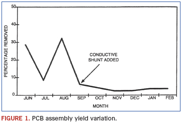
A technical assessment of the manufacturing line was undertaken, and an action plan compiled based on conventional wisdom at the time. Because of the extreme seriousness of this situation, the weekly reports were channeled to high-level executives in the company.
Initially, many extraordinary handling precautions were instituted, such as whole room ionization, bench ionizers, ESD garments, ESD chairs, constant wrist monitors, daily compliance verification, etc. Even with nearly flawless compliance to procedure, yields continued to fluctuate dramatically.
This problem was resolved with the introduction of a customized dissipative shunt referred to as a “top hat” (Figure 2). This shunt consisted of molded static dissipative foam precisely contoured to contact each lead of the device while on the circuit board. The top hat was placed on top of the NMOS device immediately after it had been assembled to the PCB. This resulted in the leads of the device being electrically connected through the static dissipative foam and static potential differences minimized.
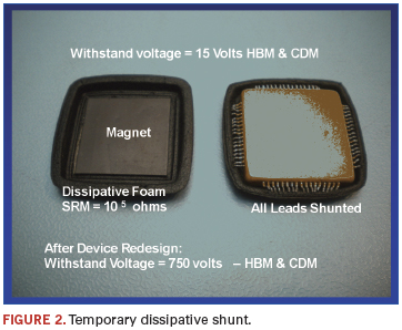
The board was then processed normally through the rest of the assembly line until it reached final test, when the top hat had to be removed. This simple addition of a shunt to the device dramatically improved yields and resulted in failure rates of less than 2%.
The simplicity of this solution is particularly striking in contrast to more common alternatives that proved unsuccessful and costly. The extraordinary measures of using a multitude of standard precautions proved to be overkill and ineffective. The solution described here introduces a simple shunt into a set of existing procedures. The incremental cost was merely $1,000 for a set of top hats. The savings realized on the production line reached $6.2 million per year for this one device on this one line and enabled a billion-dollar product line to ship on time.
Another benefit derived was the impact on the design community. Asked to justify a withstand voltage of 20V for the NMOS device involved in the project, designers responded by redesigning the device and raising the level of sensitivity to 750V HBM and CDM, a remarkable accomplishment. Some system–level design changes were made to accommodate the new protection circuitry and maintain system performance.
This case study makes clear that ultrasensitive devices pose a significant threat to production lines and may result in lost production and lost sales. The financial implications are particularly unattractive when the cost of lost sales is added to the cost of lost materials.
As a direct result of the experience outlined in this case study, minimum design requirements were modified and a new set of handling requirements for Class 0 established. It was apparent that a cookbook approach to establishing handling criteria for ultrasensitive devices would not work. For example, it is likely some of the automated equipment used in the assembly process was causing the problem. Clearly, extraordinary controls such as room ionization could not solve the problem. Adding a shunt was not only necessary, but sufficient to protect the device at great economic benefit. In addition, the manufacturing line was able to continue to operate as usual and with minimal disruption.
In conclusion, a number of valuable lessons derived from this experience have led to today’s advanced approaches for Class 0 sensitivities. First, design transfer or new product introduction checklists must include ESD sensitivities, followed by risk assessments for devices below 250V or redesign of the product to eliminate these ultra-sensitive components. Also apparent: Customized solutions are essential for cost-effective mitigation of ESD failures. Advanced auditing techniques available today such as ESD event detection and current probe analysis enable scientific determination of optimal controls and countermeasures. The final ingredient is technical expertise to conduct advanced measurements and to develop application-appropriate remedies. These lessons learned helped to create a foundation for the following case study, as well as the creation of the ESD Journal Class 0 Seal of Approval.
Case study 2: BAE Systems. This case study began during new product introductions, when ESD failures were detected with failure analysis. BAE’s Nashua, NH, site had good ANSI/ESD S20.20 controls in place. However, even one failure would be too many for this high-reliability application. So, prior to ramping up production, BAE decided to bring in external expertise to prevent any production or reliability issues.
The approach started with a baseline technical assessment, followed by customized reengineering of each critical operation, the use of quality tracking metrics and advanced technical training. The detailed process changes involved application-appropriate customization.
The baseline technical assessment is a detailed analysis of each operation, looking at HBM compliance and alignment with ANSI/ESD S20.20. This is followed by advanced auditing techniques that include a variety of ESD event detectors and high-bandwidth current probes. More traditional measurement techniques such as electrostatic voltages can be helpful, but at times insufficient to detect subtle sources of losses. Event detection and current probe measurements have become essential tools for Class 0 applications. They enable systematic modification of each manufacturing operation to be either ESD discharge event free or to exhibit events far smaller than the current failure threshold.
A multi-day workshop was conducted to elevate the users’ understanding of CDM and the technically advanced measurement techniques. Ultimately, the user must be able to fully understand Class 0 mitigation and measurement techniques. This training is reinforced with ongoing technical support for a full year to ensure the level of understanding required to achieve the Class 0 Seal of Approval.
Throughout this process, ESD Quality Metrics, including our novel Yield Risk Benchmarking methodology and meaningful quality metrics, are used to track the improvements. This enables management to set measurable goals and objectives and to efficiently monitor progress.
The benchmarking method is an accurate means of quantifying the performance of an ESD program, and there is a direct correlation to personnel compliance with ESD procedures. It has been successfully applied to hundreds of ESD programs.
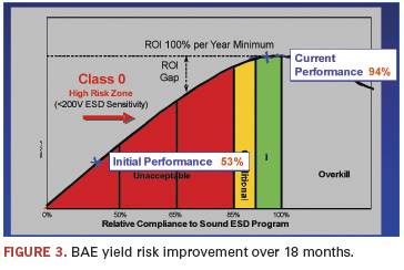
The analysis of the strengths and weaknesses of BAE’s ESD program, as well as the progress over 18 months, is reflected in Figures 3 and 4. These indexes were derived from the novel methodology and were used as a guide for improvement. Virtually all elements now reach 90% or higher. BAE’s Yield Risk Benchmarking score started at 53% and ultimately reached 94%, and its process has not experienced a single ESD failure over a three-year period since implementing Class 0 controls.
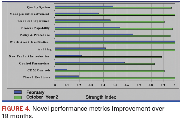
Auditing, New Product Introduction and Class 0 Readiness showed sharp improvement. Auditing is one of the more critical elements of program management, and often improvement is essential to mitigate ESD losses. Data derived from auditing can be effective in the early identification and prioritization of process deviations. These data can also be used to effectively leverage limited resources for better Class 0 compliance.
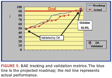
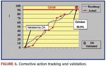
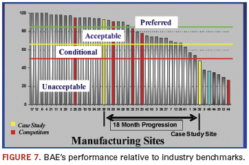
Figures 5 and 6 track improvements. Figure 5 is the novel EPM Yield Risk Benchmarking and is a reflection of the ESD Quality System improvements. The blue line is the roadmap projected at the outset, and the red line is the actual performance that was validated each month. Figure 6 is the closure timeline for the action items in the associated technical assessment. Both trend tracking metrics followed the roadmaps closely, with impressive final scores of 93.6% and 96.6%. Figure 7 illustrates the remarkable improvement relative to the electronics and defense manufacturing industries.
Conclusions
Challenges presented by Class 0 ESD sensitivities are considerable and invariably require customization of mitigation techniques. The strategy employed proved highly effective. ESD failures were virtually eliminated, and the ESD team became competent and prepared for next-generation, sensitive Class 0 devices.
Elements of a good program include the following:
- Exceptional program administration, which includes verification of the ESD performance of incoming new product designs.
- Quality metrics with tracking scores of over 90% in each category. If you cannot measure an ESD manufacturing process, you do not have a functional process! With the process outlined here, Class 0 products may be successfully produced at very high yields.
- CDM and HBM countermeasures to be executed with rigorous compliance verification and virtually flawless adherence to procedure to avoid quality or reliability excursions.
- A deep understanding of the ESD technology and Class 0 mitigation techniques, best learned through intense initial training with ongoing reinforcement over a year or more.
- CDM mitigation techniques that include both methods: minimizing voltages on the product and controlling the surface resistance of materials that contact the conductive elements of the ESDS product.
- Customized reengineering of critical operations and strategic application of dissipative materials and ionization.
- Advanced measurements such as ESD event detectors and current probes.
Ted Dangelmayer is president and CEO of Dangelmayer Associates LLC (dangelmayer.com); ted@dangelmayer.com.

LEDs are poised to take a big share of the general lighting market, with ramifications for EMS.
Over the past several years, the emergence of light-emitting diodes (LEDs) as a form of lighting for residential, commercial and industrial applications has steadily gained acceptance. While still prohibitively expensive on a cost per watt or lumen basis, LEDs are expected to reach parity with traditional forms of lighting (incandescent, flouresent and halogen) sometime around 2015. However, because LEDs have lifetimes up to 50 times longer than the standard bulb, they naturally appeal to a wide variety of commercial and industrial applications where fixed costs are high. General lighting is often viewed as the largest and last bastion of traditional lighting: Governments are legislating changes that seek to ban or phase out inefficient and chemically toxic technologies.
The total general lighting market, including lamps, ballasts, controls and fixtures, is worth approximately $55 billion and is expected to grow to $73 billion by 2015, an annual rate of 6%. The leading market segments are residential (42%), commercial (23%), industrial (12%) and outdoor (23%). Unit shipments of incandescent, fluorescent and HID lamps will give way to LED lamps, which produce greater luminosity per lamp. Although the overall lighting market declined 15% in 2009, the LED lighting lamp market grew a robust 32%. In 2010, the market started to see major outdoor area and commercial retrofit adoptions using LED modules, pushing LED penetration of general lighting to a little above 2% of the total market. Products are still highly variable in terms of quality, but improving rapidly.
To date, cost remains the biggest obstacle to LED adoption in general lighting, if cost per kilolumen is considered. Yet if costs are amortized over their entire lifetime, LEDs are cheaper than other technologies. Most people are not willing to pay the higher upfront cost of an LED light, even though it can last up to 50,000 hr. (Incandescent bulbs have an average lifetime of 1000 hr.) The initial cost and cost of ownership are expected to improve dramatically over time, however. Manufacturing LEDs is a semiconductor process that requires high tolerances, and precision process control and cost reduction are still in the early stages. Board assembly for LED light bulbs is highly automated, but involves a considerable amount of manual labor for attaching components, heat sinks and optics. The total PCB bill of materials is expected to fall by an estimated compounded rate of 34% over the next five years, as greater integration is achieved among the LED die, interconnect, packaging, circuit drivers and other hardware. Box assembly costs, including ordinary materials such as glass, plastic, reflectors and metal base, will not decline nearly as sharply.
The LED lamp assembly market is very fragmented, with companies – large and small – introducing their own lines of light engines for general illumination, which are then sold to luminaire manufacturers. Many suppliers, mostly Asian, tend to eliminate margin from finished products in an attempt to establish market share. Strong unit growth and declining ASPs combine to generate positive revenue growth, but solid earnings are difficult to achieve. Because the market is overpopulated and highly fragmented, suppliers then push costs to the margin, leaving very little for profits. There has been a slow trend toward consolidation, generally resulting in a loose collection of smaller divisions that cater to different application segments. Only multinational companies like Philips, Osram, General Electric, Panasonic, Toshiba, NEC and Hitachi are quickly building manufacturing scale and process discipline. LEDs are expected to emerge as the dominant lighting technology beginning sometime in 2015.
Though designed for local markets, manufacturing of mass-produced solid state lighting (SSL) fixtures is increasingly outsourced to low-cost manufacturers in China, Vietnam, India and Bangladesh. Hundreds of Chinese/Taiwanese and Japanese LED suppliers are looking for manufacturing scale and distribution. Outsourcing seems to be only attractive for export, except among leading manufacturers and suppliers.
Taiwanese LED chip companies like Epistar are following a foundry-type strategy. Other LED makers, such as Cree and Seoul Semiconductors, are trying to extend their business by reaching further down the value chain to LED modules and fixtures.
The Japanese are very active in the LED chip business, as well as partnering with OEMs such as Nichia, Panasonic, Sharp, Stanley and Toshiba. Panasonic in China obtains its LED light sources in the US and sends them to Chinese factories for assembly, which is cheaper than Japan. Sharp reportedly has adopted a massive outsourcing strategy to further reduce the cost of LEDs and power supplies.
The Koreans have targeted the LED market in a similar way to the LCD display market and are actively pursuing OEM component business via Seoul Semiconductor, LG Innotek and many other small suppliers. Outsourcing will likely not be the result, as vertical integration is the normal business model.
The wild-card in LEDs is Osram, which appears to be pursuing a strategy of internal manufacturing (former Sylvania with facilities in Malaysia and China) and outsourcing as long-term partners with leading EMS firms.
Foxsemicon Integrated Technology (FITI), part of the world’s largest contract manufacturer Foxconn, has formed close partnerships with major global semiconductor equipment, LED chip manufacturers and suppliers such as Charm and Ci out of Korea. FITI’s products provide a quick retrofit solution for many applications. The company is generally viewed as a competitor in LED outsourcing, similar to their component supply business.
Cree has contracted with Flextronics, the second largest contract manufacturer, in addition to plans to fill 300 jobs at its Durham, NC, LED manufacturing facility by the end of 2012. Flextronics provides final assembly services in its plant in nearby Charlotte.
The third largest EMS, Jabil, is interested in LED lighting, but only on a limited basis. It is believed that relationships with Osram and Avaga are in discussion.
Sanmina-SCI has specifically targeted LED Lighting as part of its Renewable Energy program. No assembly programs or customers have been identified, although Avago is being pursued.
In March 2010, Philips Lighting selected Elcoteq as a global growth partner of its SSL business. Elcoteq has begun production of SSL products in its factory in Dongguan, China, and expansion to Mexico and Hungary is ongoing.
For more details on the emerging market for LEDs in General Lighting, see our recently released research report, The Worldwide Electronics Assembly Market for LED General Lighting - 2011 Edition. This report sizes the market for LED chip or ICs, chip packaging, thermal management, optics, printed circuit board assembly, including drivers and related electrical components, plus final (box) assembly and test of the LED fixture for a wide variety of applications.
Randall Sherman is president and CEO of New Venture Research Corp. (newventureresearch.com); rsherman@newventureresearch.com. His column runs bimonthly.
Substrate-based IC packaging can adopt a wider range of materials, while accommodating several alternative assembly processes.
The electronics industry is experiencing a renaissance in semiconductor package technology. This is due to the growing number of innovative 3D package assembly solutions that have evolved to further enable product functionality without increasing product size. Multiple die packaging commonly uses a substrate interposer as a base. By integrating multiple die elements within a single package outline, overall product functionality has increased and been made smaller than their predecessors, improving both performance and capability. Assembly of semiconductor die onto a substrate is essentially the same as those used for standard IC packaging in lead frames; however, substrate-based IC packaging for 3D applications can adopt a wider range of materials, and several alternative processes may be used in their assembly.
Companies that have already implemented 3D semiconductor packaging have experienced success in both stacked die and stacked package methodology. Although 3D package technology has reached a level of maturity, there remain a number of issues to consider when selecting the specific methodology to be used in developing a multiple die package. The platform for mounting the die is typically one of three material sets: alumina (ceramic); a high Tg glass reinforced epoxy laminate; and, for less complex applications, one and two metal layer polyimide films. Because of the relatively high I/O required to interface multiple die, the interposers commonly adopt a uniform array configured ball or bump contact design. Limiting the semiconductor package size continues to be a factor; however, the package outline will always be controlled by the size of the largest die and number of interface contacts. The base structure (interposer) selected must furnish a surface area large enough to enable the wire-bond operation and be mechanically stable enough to withstand the process temperatures of the entire package assembly process (die attach, wire-bond and encapsulation).
Die stack assembly. When vertically stacking two or more semiconductors for wire-bond assembly, the die elements will ideally have a progressively smaller outline. This “tiered” configuration permits all die to be sequentially attached on top of one another in a single operation, leaving the edge of die elements accessible for the subsequent wire-bond operation (Figure 1). A tiered die format will generally furnish the lowest overall multiple die package profile. There also is potential for improving package performance due in part to the very short coupling between vertically configured semiconductor die. Because they generally utilize a common interposer, the package typically exhibits lower inductance and reduced overall power consumption.
When the die outlines are the same size or near the same, spacers are added between each die to clear the wire-bond features. The basic process of assembly of same size die is not unlike the tiered variation, but die attach and wire-bond operations must be performed sequentially. That is, each die is individually attached and wire bonded to the base substrate before adding a spacer and the next die in the stack and so on. Due to the limited space between die elements, conventional wire-bond loop height may not be low enough to overcome the potential interference between the bond wire profile and next-level die. Companies will often resort to a reverse-bond process typical of that shown in Figure 2. Although the die and spacer assembly method is widely used for packaging memory die, the increased complexity of the sequential stacking process does significantly impact the overall throughput efficiency for package assembly. 
Package stacking. Vertically mounting one or more packaged die (package-on-package) has evolved as a preferred alternative to die stacking for a growing number of applications. The package stacking process was initially adopted by memory semiconductor companies to provide a simple solution for furnishing significantly higher density configurations to keep pace with the more advanced processors. For DRAM applications with center located bond pads, the die element is mounted face-down on an organic interposer that is slightly wider than the die element to accommodate solder ball contacts. The wire-bond interface between the die and interposer is made from the bottom surface of the interposer followed by encapsulation, solder ball attach and test. The module configuration in Figure 3 exhibits four vertically mounted DRAM die package sections, using only the edge-located solder ball contacts for mechanical and electrical interface.
Developing a multiple die, system level package with related but dissimilar functions within a single package outline will enable greater PCB surface utilization and potentially provide enhanced electrical performance. In reviewing a typical system application for a personal GPS product (Figure 4), it is apparent a number of candidate semiconductor functions could be integrated into a common 3D package configuration. To minimize product size and optimize the PCB area utilization, it is conceivable to combine a number of closely related functions into four or five package-on-package assemblies.
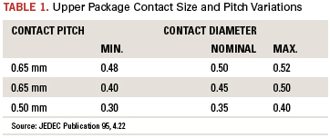
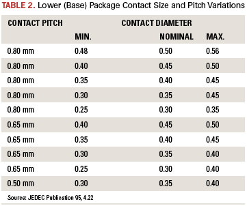
A likely configuration for package stacking would begin with the processor die element packaged onto the base substrate. This processor die will have significantly more I/O than any other closely related semiconductor functions may be mounted face-up for wire-bond assembly or (after wafer level redistribution and bumping) mounted face-down for direct solder attachment. The second-level package layer will most likely furnish the memory functions. In the GPS instance, for example, SDRAM and FLASH/ EPROM functions are directly interfaced with the processor units. Packaging memory using the die stack process described above is preferred for the upper section because wafer level fabrication, when mature, is a high yield process. The lower-packaged processor, on the other hand, is most often packaged solo because the processor will require very specialized electrical test methodology before joining the sections. The example in Figure 5 illustrates the now familiar package-on-package configuration for mixed function applications. The JEDEC-defined ball contact pitch and diameter variations developed for each section of the package-on-package family are furnished in Table 1 and Table 2.
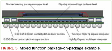
Other candidates for 3D packaging on the GPS example include the RF/IF components, the display drivers, audio, power management and signal conditioning elements. They may be packaged using either die stack or package stack or a combination of both, depending on die level yields and electrical test complexity.
Although the benefit gained with 3D semiconductor packaging is very high, a number of challenges will need to be addressed. In addition to selecting a competent supplier for package assembly and test, users need to consider the reliability of the supply chain for the die elements selected. Further, before performing assembly, whether stacking die or stacking packaged die, the package assembly specialist often will want to reduce the die elements’ thickness. Thinning of the individual die units contributes to process uniformity and enables the reduction in overall package height. The thinning process, however, is performed while the die elements remain in the wafer format. Some semiconductor suppliers are reluctant to furnish full wafers to outside sources, though, because the thinned wafers are more difficult to transport. Additionally, if die elements are supplied to the assembly service company already singulated, the fabricator may be reluctant to perform any special thinning services that may affect yield.
Embedded components. The process for embedding components in the PCB substrate is not new, but semiconductor companies are now adopting the methodology in high volume using wafer-level operations they refer to as “fan-out WLP.” All the packaging operations are performed sequentially at the wafer level. Additional area must be provided to extend the package size beyond the IC surface area to allow for increased solder ball population and a contact pitch more suitable for conventional SMT assembly processing. The die element embedded within the substrate interposer’s “core” section (Figure 6) is a relatively robust 150µm in thickness, but many companies are thinning die down to 50µm to further minimize substrate thickness. In regard to the SMT ball pitch furnished for assembly, 0.50mm has been the norm for a majority of the array configured components, but 0.40mm ball pitch is not uncommon.
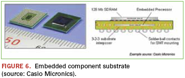
Package performance. Designers are well aware that the shorter the circuit interface provided between the individual die elements, the greater the signal transmission speed. By embedding the semiconductor on an innerlayer directly in line with a related semiconductor package mounted on the outer surface, the conductor interface can be minimized. With the die element mounted within or onto the substrate interposer’s core layer, resin-coated foil is laminated over the area to enable circuit interface to the layers above. The interface is made through small microvias that are laser ablated and plated directly to the bond-sites of the die element. Additional RCC layers are built up on the substrate’s base sequentially to complete the interface to the outer surface layers of the interposer. When die elements are prepared with bump contacts, the die can be mounted face down onto a mating contact pattern for solder or conductive polymer attachment. Several PCB suppliers with experience in buildup circuits are involved in embedding both passive and active components. A majority of companies furnishing embedded component substrates in high volume are located in Europe and Asia, but there are number of capable North American suppliers as well.
Concerns
Testing 3D die-stacked packages with mixed function die has been a serious defector because of the unique testing requirements of dissimilar functions. Combining logic functions with memory in a single package outline, for example, has always proven difficult. This is because testing and burn-in requirements for memory devices are very different than that required for the logic functions. Additionally, when several functionally different die elements are stacked within a single package outline (die-stack), the differences in die sizes and the die quality can adversely affect package assembly yields. Package-on-package products, on the other hand, permit functional test of each section before joining. Test before joining has proved far more practical both for suppliers and users because the sections can be supplied as separate units and joined at the board-level assembly stage, or furnished as a single package-level product, thoroughly tested and certified to be ready for PCB mounting.
PCB assembly issues. Users of the PoP product have experienced a number of challenges. The multiple level package families, when furnished on an organic substrate, are more sensitive to the effects of the thermal profile developed for reflow solder attachment. Users have experienced excessive warping of the package substrate sections, typically occurring during reflow solder heating. As the substrate temperature exceeds the point of glass transition, the rigid resin-based laminate relaxes somewhat, permitting the material to reach a condition that can result in deformation. The deformation is most prominent at the outer edge area and corners of the substrate sections. When the warping results in the substrate deforming away from the circuit board surface, solder joints can elongate or separate from the opposing surface. When the substrate warps downward at the edge or corner areas, the contacts will compress, often forming a common connection or short between adjacent contact sites. Both conditions can be avoided by refining the reflow solder profile. The temperature level and timing is dependent on individual assembly complexity and the specific reflow oven used. Many have found, however, that when the materials are exposed to a gradual thermal rise through the solder’s liquidus threshold and peak temperature, substrate warping is minimal and self-correcting.
Embedded component process issues. When producing an organic substrate for the package, module or unit, a reliable infrastructure must be in place to accommodate the manufacturing processes. One key issue is ownership, especially for the embedded active die elements. Due to the number of process steps involved throughout the embedded component fabrication operations, the component parts will be subject to damage. Ideally, the originating companies will bring together the two primary suppliers: the circuit board fabricator and the contract electronics assembler. Some companies may have already established both these capabilities, but others will need to develop partnerships. These partnerships must be willing to adjust their portion of the generated revenue against the overall process yield. That will include sharing losses from fabrication process defects and damaged components.
Economics
Economics has a significant influence on key materials used in 3D semiconductor packaging. The primary element affecting package cost is the substrate interposer. Because of the relative complexity of the newer generations of high-performance semiconductors, I/O counts are expanding. To control the outline limits of the die element, semiconductor designers are reducing the wire-bond contact pitch to less than 50µm. To prepare the die for flip-chip mounting and enable surface area on the substrate for efficient circuit routing, the wire-bond contact sites must be redistributed to a more uniform array format. Flip-chip configured die are commonly furnished with contact spacing in a range from 0.50 to 0.40mm pitch. These contact sites are generally furnished with a raised, solder-compatible bump, sphere or post feature for reflow solder attachment. As the array contact pitch approaches 0.35 and 0.30mm, however, conventional placement and solder attachment methods will be more difficult. Three types of interconnects are currently in use for very-fine pitch flip-chip die: high-Pb alloy bump, Pb-free bump and copper post. The high-Pb bump is being phased out due to RoHS requirements, and Pb-free bump is somewhat limited due to solder collapse. Additionally, the widely used SnAgCu alloy composition is prone to void formation due to electromigration.
The copper-post-on-die contact has evolved as a viable solution for a number of high-performance semiconductor applications because it enables very-fine pitch (<0.40mm) capability. Some issues with copper-post-on-die, however, are the relatively high cost of wafer level processing and uncertain physical integrity, especially when mounted onto extremely low-k dielectrics. The typical failure mode seen in all of these very fine-pitch flip-chip interconnects is related to solder joint fatigue, cracking and voiding in the solder interface. Voiding is often due to the effects of electromigration, a result of long-term exposure to high current densities. An alternative substrate interconnect solution has been developed to address these troubling product reliability issues, while offering a roadmap to fine-pitch flip-chip contact spacing well below 100µm. The µPILR substrate (Figure 7) was developed for one of the new generations of high-end processors. The substrate has an array of 10,132 solid copper pillars on 150µm and 200µm pitch. In this example, the solid copper µPILR contact features are integrated onto a 10 layer (3-4-3) organic substrate structure that measures 40 x 40 x 1.2mm thick.
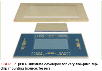
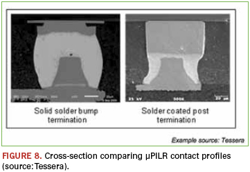
Because the contact formation is part of the substrate fabrication process and manufactured using conventional industry equipment and materials, additional cost for furnishing the raised contact array is minimal. Depending on the method of manufacturing, these interconnects can be furnished in different sizes (diameter and height) and shapes. Furthermore, the flip-chip to µPILR substrate assembly process requires no special consideration beyond that normally used for mounting very-fine-pitch configured die. Because the solid copper contacts are NiAu-plated, a flip-chip configured semiconductor die with either solid solder bump or solder alloy coated copper post contacts will enable a uniform and reliable solder joint (Figure 8). In regard to the effects of electromigration, the µPILR contact has exhibited no significant voiding or cracking in the solder interface, even when exposed to high current density conditions.
Note: µPILR is a trademark of Tessera Inc. or its affiliated companies in the US and other countries.
Vern Solberg is an independent consultant specializing in SMT and microelectronics design and manufacturing technology; vsolberg123@aol.com.
Relying on inputs is no longer necessary.
I like to sum up the goal of stencil printing in one simple phrase: Get the right amount of solder paste in the right spot – every time. Any engineer who’s done a stint on a production floor knows that’s much easier said than done. You need the right paste, the right printer setup, the right ambient environment, the right operators and technicians, and the right stencil.
The right stencil starts with the right stencil supplier, but with all the options in metals, manufacturing processes, frame styles, price points and marketing claims, selecting a stencil vendor can be a considerable task, even for a seasoned professional.
Factors in the vendor qualification process should include technological capability, proximity to the assembly house, delivery times, and most of all, quality. While price is sometimes a factor, I personally don’t put a lot of weight on it, because given the influence of a relatively low cost piece of tooling on the high cost of rework, a $50 or $100 difference in purchase price can be recouped in a single shift of defect avoidance.
For years, engineers measured the quality of a stencil by measuring the stencil itself – checking aperture size and location, aperture profile, wall smoothness and foil thickness uniformity. In areas where stencil quality really mattered – the fine features of miniaturized packages – we relied on measuring the input variables of dimensional accuracy. But white light-based solder paste inspection gives us the ability to judge stencil quality based on its actual performance. We can look at the outputs rather than the inputs. And the output – the right amount of paste in the right spot – is what stencil printing is all about.
Empowered with accurate paste volume measurements, we no longer have to painstakingly measure stencil geometry and interpret its influence on process quality. We’ve got a tool that provides hard, irrefutable data on which product provides the best print quality.
When Ray Whittier of Vicor (vicr.com) wanted to choose a vendor, he listed the factors deemed important to his assembly operation, surveyed the supply base, and arrived at a short list of four potential suppliers. He sent artwork to get demo stencils manufactured and began qualification tests. His print operation is fairly challenging because most of his components are miniature ones.
Whittier ran test prints on his NPI line, and used his solder paste inspection system to evaluate print quality. For the tests, he took all the typical precautions to isolate the stencil as the only variable (same paste from same lot, freshly dispensed with four kneads for each stencil, back to front stroke only, dummy boards between test prints, stabilized temperature and humidity, etc.), and measured 10 prints for each stencil. The analysis looked at print yields and at volume repeatability for 0201 and 0.5mm BGA components. Table 1 summarizes the findings.
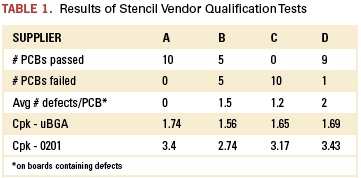
Supplier A provided the best-performing stencil, which produced 100% yields on the 10-board test and showed the best volume repeatability. Supplier D ran a relatively close second, with similar repeatability, but produced one bad print that contained two defects in the test of 10 prints.
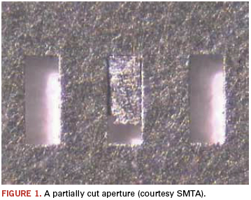
Supplier D was immediately disqualified from contention because the evaluation stencil was missing an aperture. Given that these designs pack about 10,000 apertures in a 4 x 12" area, the missing one could have easily gone unnoticed if the inputs (sample aperture size and location) were measured rather than the outputs (all deposit volumes) of the stencil.
The performance of Supplier B’s stencil was unacceptable: while its volume Cpks were only slightly lower than the others’, its overall print yields were a dismal 50%. It really doesn’t matter that the failed prints only contained one or two bad deposits (a defect rate of 100 to 200 ppm); it takes only one to scrap the entire print.
If only all engineering studies produced such clear and concise data! Whittier’s decision is obvious: Stencils from Supplier A produce the best, most consistent quality prints, making them the primary source. Supplier D is close behind and qualifies as the secondary source. And B and C? Not viable.
By using an SPI to help measure stencil performance, Whitter
1. Identified the best sources for this critical piece of process tooling.
2. Set a performance baseline to which he can compare future stencil performance studies.
3. Increased the level of control on his printing process, and therefore, the probability that he’ll meet his goal of depositing the right amount of solder paste in the right spot more often.
And the best part? The data generation speed: The 10-print stencil characterization test only takes about 20 min. of line time, so it can be accomplished during a product changeover or a lunch break.
Ed.: Due to an editing error, the third paragraph of Chrys’ April 2011 article (p. 44) misstated the aperture sizes. The proper sizes are 0.012”, 0.013” and 0.014”. We regret the errors.
Chrys Shea is founder of Shea Engineering Services (sheaengineering.com); chrys@sheaengineering.com. She wrote this article on behalf of Christopher Associates (christopherweb.com).
