

Our newest columnist extols the low energy use and repeatability of VPS.
Vapor phase achieves a very gentle, reliable and repeatable reflow process. Due to its excellent heat transfer capability, vapor phase systems typically consume low amounts of electricity and Galden fluid. (Galden refers to the inert, fluorinated fluids used for heat transfer in vapor phase soldering machines.) Vapor phase machines also tend to have low operational costs and maintenance requirements. They use two chambers and cooling systems to help prevent the escape of vapor and heat. The vapor is under constant condensation and recirculates to minimize fluid consumption. Galden liquid is non-aggressive, noncorrosive, non-electrically conducive, completely inert, and environmentally friendly. It is important to mention that Galden has no expiration, and the material never has to be replaced or disposed.
The power consumption of a vapor phase machine is much lower than any other reflow systems. Higher-end machines use an average of 10 KVA per hour, much lower than any forced convection reflow ovens. A vapor phase machine utilizes 98% of the heat created to heat the assembly, whereas for other reflow processes much of the heat created is not utilized to heat the assembly. Instead, the heat escapes other reflow systems, adding to plant air conditioning costs. Recommended maintenance can be as infrequent as once a year for a single-shift operation and twice a year for a two-shift operation. Preventive maintenance costs also tend to be very low because the main parts are situated outside the heating chambers.
There is a misconception that the cost of Galden fluid increases operating expenses. However, advancements in vapor phase machines have served to minimize fluid consumption. In addition to the electricity savings and nitrogen savings, VPS eliminates yet another cost. Nitrogen use is very expensive, and it requires additional process control and storage. With vapor phase, the atmosphere is inherently completely inert (oxygen-free), providing huge cost savings for companies that use nitrogen.
Vapor phase is an ideal solution for the transition to Pb-free. Pb-free solders tend to have higher melting points. Overheating components and assemblies is physically impossible due to the boiling point of the Galden. The even heat transfer results in much lower peak temperatures and lower delta Ts. Overheated and damaged components can have short-term and long-term cost impacts. Also, due to the even heat transfer, a high-mix environment requires fewer profiles. If coupled with real-time profiling capabilities, no additional external profiler is required. With temperature-driven process control, the profiles are repeatable all the time, and there are fast changeovers even, from leaded and Pb-free processes.
For prototypes and small-volume production, tabletop and batch vapor phase systems have a much smaller footprint than other reflow systems. In a tabletop unit, BGAs and fine-pitch components in Pb-free assemblies can be soldered with very low delta Ts and very low peak temperatures. In addition to the floor space savings, these smaller tabletop units use only 1.5 KVA per hour.
Ed. note: This continues our series on various machine soldering processes. To date, we’ve covered convection reflow, wave and selective. Since 2009, Jochen Lipp has been CEO of IBL Technologies, a maker of inline vapor phase soldering equipment. Prior to joining IBL, he spent nearly 10 years as vice president of operations and COO of Epic Technologies, a multinational EMS firm, where he developed and implemented the EPIC Synchronous Flow Model.
Jochen Lipp is CEO of IBL Technologies (ibl-tech.com); j.lipp@ibl-tech.com. His column will run bimonthly.

Intelligent SPI feedback moves the process closer to true “lights out” printing.
Printer know-how? People have knowledge and intuition, but machines? You may be skeptical after reading the first 10 words of this column, but bear with me. I’m confident that, by the end, you’ll agree that printers can, indeed, learn.
Know-how, or learned knowledge, comes with experience, and that is precisely what some innovative printing technology is designed to deliver: a “smart” printer that can make informed decisions about required adjustments. Working in tandem with solder paste inspection (SPI) technology, printer software has been engineered to assess SPI data with a high level of process reference and, using that input, auto-correct when required. This certainly isn’t the first time such a system has been attempted, but, in my view, it’s the first time the software and the SPI technology have been robust enough to enable meaningful and yield-enhancing results.
What’s changed to make this technology now viable? First, the demand brought on by miniaturization. In the world of 0.3mm CSPs and 01005s, there is little room for error; paste pretty much has to be spot on the pad, or you are going to have process issues. When pitches were a bit more forgiving, closed loop – and SPI systems, for that matter – were a “nice to have.” But, now, alignment correction is a near necessity for a good process.
The second factor that has made closed-loop printing more attainable is the advance of SPI capability. In the past, technically superior SPI systems were also very costly. Today, sophisticated SPI technology that provides accurate data for paste height, area, volume and alignment is available at a price point acceptable to the market.
The convergence of these two factors now makes closed-loop printing an effective reality. But, of course, the simple task of a printing platform reading SPI data is not beneficial to the process engineer. The value is the know-how and the process expertise that’s built into the printer software. This allows the print platform to make adjustments only if warranted by process trend analysis. What you don’t want – and what older-generation systems may foster – is oscillation. If a machine is constantly overcorrecting – 50µm one way for one print and then 50µm the other way for the next – then the printer is never settled and the process somewhat out of control.
If, however, the printer software can act just like a responsible production engineer – that is to say, not respond to the first misaligned deposit with a knee-jerk reaction – the process will become far more stable, reliable and self-controlled. This is precisely the type of logic and intelligence that is coming online today.
Here’s how it works. The printer takes multiple data points from the SPI feedback, analyzes them and, if required, adjusts the offset (alignment) accordingly. Communication is on-the-fly and seamless so that no additional throughput overhead is introduced. Data are constantly fed to the printer, which is trending the data against programmed process expertise and making corrections when required. Just to be clear, though, the SPI system is still the gatekeeper on the process; the printer isn’t controlling the SPI. What the technology aims to do is ensure that the SPI doesn’t have to flag a board and stop the line. Manufacturers will set their own tolerances and upper limits for each device on the SPI system. The printer offsets, logically, are then set at less than that. So, there is a tighter limit on the printer and a wider limit on the SPI.
As an engineer, I have to admit it is difficult to stand back, be totally hands-off and observe the system do its thing. I’ve witnessed many a production engineer become anxious while watching closed loop in action, and I know they are wondering, “Is it doing anything?” And then, voilà, they see the results. Printers can, indeed, learn and use that knowledge to improve the process. Offset correction is just the beginning; there is a lot more that print platforms can learn, and future assembly operations will be all the more efficient for it.
Clive Ashmore is global applied process engineering manager at DEK International (dek.com); cashmore@dek.com. His column appears bimonthly.
Board Fabrication
“Development of Optical Interconnects with Polymer Waveguides for High-Speed Electronic Systems”
Author: Marika Immonen; marika.immonen@meadvillegroup.com.
Abstract: This paper describes the fabrication and characterization of optical/electrical printed circuit boards (O/E-PCB) with embedded polymer waveguides for 3D optical interconnects. Optical circuitry is built up on PCBs using UV lithography; 45° input/output (I/O) couplers are fabricated by inclined exposure. Commercial polymers are used as optical core and cladding materials. Critical mirror properties of angle, surface quality, reflectivity and coupling efficiency are characterized. (HKPCA, December 2011)
“Wrap Plating for Blind and Buried Vias”
Author: Dale Lovell; dalel@innovative-circuits.com.
Abstract: Wrap plating is a manufacturing step for producing blind and buried vias in printed circuit boards. Wrap plating helps increase via-in-pad reliability by depositing copper in the via hole and around the surface foil. This presentation describes the process, and includes certain aspects of bare board processing, such as innerlayer etching, plasma, layup, laminating, drilling, planerizing, tin strip, immersion gold, soldermask and button (spot) plating. (Printed Circuit University, August 2011)
Component Packaging
“Evaluation of Reliability and Stack-Up Height on Next-Generation 0.5 Mm Pitch PoP”
Authors: Mark Schwarz, Alan Choi, and Owen Fay; mschwarz@qualcomm.com.
Abstract: There is a push from the end-user to make the package-on-package (PoP) stack-up thinner. The overall height of the tallest package mounted on the PCB, often the PoP, becomes the major factor that dictates product design thickness. This paper explores different configurations of the bottom PoP component, while holding the memory component constant. The lower package is 14mm in size, uses a 0.4mm bottom pitch with 904 solderballs. The top package is also 14mm, with a 0.5mm pitch with 240 solderballs. The interconnect between the packages is joined through soldered connections embedded within vias of the bottom package’s mold compound. Three bottom solderball diameters were characterized as a drop-in solution to decreasing overall package thickness. Selected package configurations were evaluated based on drop shock, thermal cycling and cyclic bend reliability test, focusing on both the bottom and top PoP interface. Two mold compound via dimensions and two topball solder alloy compositions were studied for their effects on total collapsed height and reliability. Coplanarity and high-temperature warpage for the various configurations were also monitored. (SMTA International, October 2011)
PCB Design
“Conquering High Pin-Count Devices with Fan-Out and Escape Routing”
Author: Andy Buja; andy.buja@zuken.com.
Abstract: Consumer electronics is highly driven by more features in the same or smaller packaging. As a result, designs have an increasing number of high pin-count devices. Many of these are configurable FPGA devices. Less real estate is available to route these devices, and routing of these components is key to design completion. This presentation focuses on available tools to optimize this process. (ZDAC, November 2011)
“Why DfM?”
Author: Darren Hitchcock; darren.hitchcock@multek.com.
Abstract: Valuable tips on designing printed circuit boards with the manufacturer in mind. Explains how to design PCBs cost-effectively using existing manufacturing processes and equipment. Also includes helpful tips on improving quality, yield and performance, and reducing lead time. (Printed Circuit University, November 2011)
This column provides abstracts from recent industry conferences and company white papers. Our goal is to provide an added opportunity for readers to keep abreast of technology and business trends.
A step-by-step matching of process to product type.
Automated selective soldering is a viable approach to enhance the affordability of certain electronics manufacturing operations. This step-by-step approach to selective soldering is meant to help decide which method is best.
Step 1: Decide if automated selective soldering can improve affordability in your product. Does the circuit card assembly mix surface mount technology and plated through-hole? A “yes” is imperative for selective soldering to be economically viable. Most cases of selective soldering are instituted to accommodate a small number of plated through-hole components usually manually soldered in an otherwise predominantly surface mounted assembly. These components are typically electrical connectors or high-power supply components available only in PTH versions.
Manual soldering is the obvious alternative and is typically used for prototyping a new assembly with a few PTH components. Because there is an inherent inspection operation in any manual soldering application (by the operator doing the soldering), an automated selective soldering operation requires a planned inspection step to maintain acceptable joints.
At this juncture, also ask, Is the product high- or medium-volume or is the product high-mix/low-volume? The answer will indicate the appropriate hardware and software combination to secure the most cost-effective automated selective soldering operation.
Step 2: Decide which type of selective soldering will be most effective:
- Selective aperture pallet (masked) wave.
- Mini solder wave with mask.
- Programmed solder fountain.
- Programmed laser.
Selective aperture pallet (masked) over wave solder. This is the simplest form of selective soldering, but must be balanced between the need to do selective soldering and production wave soldering. The selective aperture fixture effectively masks the areas previously soldered in the SMT reflow and non-selective wave soldering process, while exposing only those areas to be selectively soldered. The fixtured PCB assembly is then passed over traditional wave soldering equipment to complete the process. While each fixture is specific for a PCB assembly, wave soldering is a routine operation that is very cost-effective for small-volume/high-mix assembly.
Mini solder wave with mask. For higher volumes of product requiring selective soldering, the investment in smaller, dedicated wave solder equipment is economically justified by increasing production wave solder equipment availability.
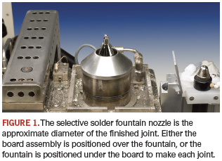
Programmed selective solder fountain. This process is slower than the two previous methods, but much more accurate in terms of solder volume and joint quality. A small fountain of molten solder (Figure 1) is pumped to each through-hole joint of the PCB. The PCB may be fixed and the solder fountain moved underneath the PCB using a precision, three-axis programmable gantry, or the PCB may be positioned over a stationary solder fountain. CAD-based board layouts can be imported to accurately position the board and solder fountain. Since each solder joint can be individually created, no unique fixturing is required. This technique requires both dedicated hardware and software and can be justified for extremely low-volume/high-mix applications.
Laser selective soldering system. Instead of a solder fountain, the laser selective solder system uses CAD data to position a laser (with solder wire feed) and directly solder any point on the board. The major advantage is the elimination of thermal stress to the surrounding board area. This noncontact soldering process produces consistent high-quality solder joints at typically one per second with maximum flexibility. It may even be possible to eliminate stencils and solder masks from the board to reduce manufacturing costs. This represents the most costly, but most productive method of selective soldering for very high-mix, very high-volume manufacturing.
Step 3: Select flux application method. Regardless of selective soldering equipment, there are two types of selective flux applicators: spray fluxer and dropjet fluxer. The spray fluxer applies atomized flux spray to a specific area, while the dropjet fluxer has more precise control over flux volume and PCB position. The final choice depends on the circumstances surrounding the soldering application.
ACI Technologies Inc. (aciusa.org) is the National Center of Excellence in Electronics Manufacturing, specializing in manufacturing services, IPC standards and manufacturing training, failure analysis and other analytical services. This column appears monthly.

The benchmarks are aggressive, but progress is being made.
What sits at the foundation of widespread solar adoption is no huge secret: The technology has to be inexpensive (relative to fossil fuel power generation), broadly available, reliable long-term and self-sustaining. So, it’s not so much what lies at the end of the road that’s debatable; it’s the milestones along the journey that warrant discussion.
The recently published International Technology Roadmap for Photovoltaics (ITRPV)1 sheds light on the aggressive advances in all areas – material use, manufacturing equipment output and process developments – required to significantly reduce cost and raise efficiency of solar-generated electricity. The study, which centers on crystalline-silicon (c-Si) solar cell/module processes and materials (c-Si cells, incidentally, account for nearly 80% of today’s installed solar modules), points out that while the cost of solar modules has been reduced by about 17% to 25% (according to its historical learning curve), this trend has to continue at an aggressive pace over the next decade in order to achieve the overall cost-reduction goals. Among some of the eye-opening, cost-lowering strategies outlined in the report are silicon price reductions of 50% or more (until 2020), new manufacturing equipment and processes that can cope with much thinner wafers (part of the 50% silicon price reduction scenario), development of Pb-free pastes that deliver equal or better performance to current materials, silver consumption reductions, equipment throughput capacity improvements and new cell designs and technologies. Whew! That’s a lot to take in on this road trip.
Is all this achievable and, equally important, attainable in a respectable time frame? Yes and yes. In fact, the good news is that much of this work is already underway and considerable progress made toward achieving these objectives. Of course, my expertise lies with the cell metallization process and, speaking from a relative position of experience, metallization and printing techniques are, in some cases, ahead of what the ITRPV outlines.
Let’s start with the silicon cost-reduction strategy and the corresponding wafer handling criteria. In addition to the base price of silicon being reduced, most of the silicon overhead savings is to be achieved through the use of thinner (i.e., less silicon) wafers. The ITRPV report cites current average wafer thicknesses at 180µm, moving to 160µm in 2012, and by 2020, the wafer thickness needs to be at 100µm to achieve the proposed 50% silicon cost reduction. For the manufacturing side, that means being able to handle delicate substrates, while ensuring very low breakage rates. Solutions already developed include metallization platforms with zero-edge-contact handling, wafer transport systems that delicately load/unload wafers, and materials deposition strategies that permit robust paste transfer with exceptionally controlled pressure to eliminate breakage concerns.
Silver consumption decreases and finer line printing are also two areas of the cost-competitive strategy outlined by the ITRPV. The report suggests reducing paste consumption in the near term (the next one to three years) to help lessen the impact of high silver costs and, in the longer term, moving to Cu-based materials. In September, I addressed the silver conundrum and outlined how technologies such as print-on-print (PoP) and dual print, along with a change of materials, can significantly lower cost. This is precisely in line with the ITRPV data. Not only does the PoP approach apply to silver reduction, but also addresses the piece of the technology roadmap that calls for finer-line printing and line width. PoP effectively narrows the width and raises the conductor finger height so that less shadowing occurs without a sacrifice to conductivity and efficiency. This technique recently made headlines when the Institute for Solar Energy Research Hamelin (ISFH) reported that PoP technology was a central component to its record-setting 19.4% cell efficiency.2 Currently, the finger width for PoP sits at 60µm. The ITRPV calls for that measurement to be reduced to a mere 30µm, with alignment accuracy better than 10µm for more complex cell structures by 2020. In a lab environment, our company has demonstrated 50µm PoP finger widths, with dual-print widths down to 35µm.
Not surprisingly, cell production is going to require large economies-of-scale to meet cost-reduction targets. Translation: greater equipment throughput for both front- and backend cell processes, plus matching, equal capacity for both process areas. I can’t speak for front-end chemical and thermal equipment companies, but I can certainly comment on metallization throughput. The current roadmap has set a metallization/classification throughput target of 3600 wafers per hour (wph) by 2013, doubling to 7200 wph by 2020, an objective we are well on track to meet.
There also are several other critical components in the drive toward solar cost-competitiveness. These include new higher efficiency, lower cost assembly cell designs, such as back contact (MWT and EWT) and efficiency-enhancing technologies like selective emitter (which, incidentally, requires extremely accurate printing for a good result), among others.
Buckle up! The ride is going to be intense, but rewarding.
References
1. International Technology Roadmap for Photovoltaics Results 2010, Second Edition, March 2011.
2. “DEK Solar Helps Enable Record 19.4% Cell Efficiency at ISFH,” DEK press release, May 2011.
Tom Falcon is a senior process development specialist at DEK Solar (dek.com); tfalcon@dek.com. His column runs bimonthly.

Diversity programs don’t have to be overhead-intensive, just inspiring.
Picking up from our December column, another recruiting/developmental resource is MentorNet. SMTA partnered with MentorNet in 2008 to meet an increasing demand for mentors from student members, and for SMTA members to connect with students studying in related fields. This partnership allows members access to resources offered by MentorNet: one-on-one email mentoring, résumé database for student internships and jobs, and the E-Forum.
The MentorNet E-Mentoring Program is designed to provide information, encouragement, and support to community college, undergraduate and graduate students, fellows and untenured faculty. Protégés are matched in one-on-one e-mail relationships with mentors who have work experience, and MentorNet provides the training, coaching and support for a successful eight-month mentoring relationship. Karen Bergseth (karen@smta.org) is the contact for more information.
During the networking event (see last month's column), Bergseth made the very valid point that MentorNet needs students as much as mentors. Don’t be afraid to mention this resource to your college-bound children, extended family, friends with technically-inclined kids, and educators, because far too many students enter college with no idea of what it takes to be successful in engineering or the resources available to help them get a head start on building relationships that can lead to future employment. With all the changes and challenges in education, students can’t afford to make a mistake in some of their course/career choices, and a mentor can help define the path or at least light the way.
While these programs help to ensure a solid educational foundation at the entry level, which is essential to starting on a level playing field, it is also important to keep that field level over time. Questions to ask in evaluating corporate practices in this area include:
- Are corporate values and desired behaviors clearly stated?
- Is the employee evaluation process tied to specific goal achievement?
- Are offsite networking opportunities exclusionary to any otherwise qualified individuals?
- Is there a coaching, mentoring or buddy system in place for new employees?
Diversity programs don’t have to be overhead-intensive. Instead, they just need to inspire a commitment to non-biased talent development within the management team. The company I felt most equally treated in didn’t have a diversity program. It just had clearly-stated performance goals and everyone was judged on performance to mutually-agreed upon goals. I was the only woman in senior management, but I always felt I was viewed solely as a member of the executive team. That positive impression started in my first two weeks on the job when I was scheduled for lunches every day with individual members of senior management and the board of directors. Over lunch we discussed the organizational challenges they saw as most important, my impressions and workable solutions. That upfront informal interaction laid the strongest foundation I’ve ever had in an organization, and it was part of an internal effort to better integrate new members of the team. When I’ve talked with female engineers, the most frequent comment I hear is that they just want to be considered team members vs. being treated differently in terms of team interaction because they are women. The casual social interaction I’ve just described is not done enough cross-gender, and many women are uncomfortable trying to initiate it.
Top talent comes in many forms. Companies that focus on attracting the right talent and then growing those individuals have a competitive advantage. The group of women I met at the networking reception was comprised of several generations, and it reminded me of just how much both the electronics and EMS industries had improved in talent development. However, thinking about some of the challenges and barriers that we “early adopters” chose to overcome as the industry evolved motivated me to write this article. Younger women, find an older woman in your organization and thank her for helping plow the road. It’s good to see the path less travelled turning into a highway. More important, it is refreshing to see a group of women comfortable enough to gather in a room and share their experiences. That alone highlights just how much better things have become.
Susan Mucha is president of Powell-Mucha Consulting Inc. (powell-muchaconsulting.com), and author of Find It. Book It. Grow It. A Robust Process for Account Acquisition in Electronics Manufacturing Services; smucha@powell-muchaconsulting.com.

Press Releases
- Zollner Puts a New Mechanics Building into Operation
- Changes in Incap’s Management Team: Incap updates its leadership model to support its growth strategy
- Niche Electronics Celebrates Completion of Florida Expansion
- Microscreen Names Nik Thomas Director, Expands Leadership Role Amid Continued Organizational Growth