


Electroplated tin leads are not desirable because of the risk of whiskering.
There are a number of reasons to re-tin components from the stockroom prior to attaching them to an assembly. One example is the following: When building a high-reliability assembly using traditional Sn63 solder, one of the components is only available in a RoHS-compatible finish: in this case, electroplated tin. What to do? If the component is plated with tin, shouldn’t it be compatible with SnPb solder?
Well, not exactly. The added volume of tin in the plating, however slight, will change the percentage of tin in the solder joint, creating a new alloy that may have undesirable characteristics, such as being more brittle. The other reason for hot solder re-tinning is to prevent formation of tin whiskers, which tend to grow out of a plated finish, but won’t grow out of a fused alloy finish applied through dipping in hot solder. One cannot simply solder a component with Sn-plated leads to a circuit intended for military use, because any portion of that lead surface not wetted with solder has potential for tin whisker growth and catastrophic failure through shorting.
Therefore, what one has to do is remove that pure tin plating and replace it with a fused finish of the same solder alloy that is going to be in the connecting solder joint. This is the typical method of converting modern components born after RoHS with Pb-free finishes compatible with SnPb assembly, usually found in high-reliability or military applications. (Since RoHS, fewer components are available with SnPb finishes.)
If not plated with pure tin, these components may also have a gold plating finish on the leads that must be removed. Gold in the solder joint can lead to a phenomenon known as gold embrittlement. In the tinning process, these components, whether tin- or gold-plated, are dipped in a pool of solder to wash away the undesired plating. The components are then re-tinned with a SnPb finish.
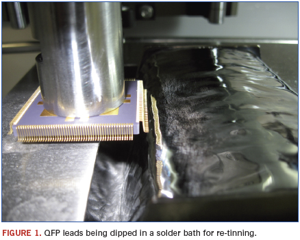
The tinning process basically involves the use of two solder pots, the first one being the “sacrificial” pot that removes the unwanted plating of gold, tin, or other alloy. The second pot is the “virgin” pot that contains the alloy to be applied to the component prior to assembly. Essentially, the component is picked up, dipped in flux, then dipped in the first pot to remove the unwanted plating. During this initial dipping, the tinning system should employ some manner of agitation in the pot to produce a scrubbing effect for complete removal of the unwanted metallization.
The component is then fluxed again and dipped into the virgin pot to apply the new fused finish. The component isn’t dipped flat, but is tilted, so that one side is dipped at a time. This is done primarily to prevent icicling, for a clean peel away of the solder. Inerting is also used to minimize icicling, particularly when using Pb-free alloys. Using an automated process ensures repeatability and consistency of results, and reduces the chance of operator-induced damage to fine-pitch leads. Dipping times for plating removal and re-tinning average about 2 sec. for each row of leads. Also, flux is applied through a dipping process to ensure uniform application and thorough fluxing for proper wetting.
Thus, the process, from removal of the component from the tray, through fluxing, preheating, dipping, visual inspection, followed by post-cleaning and washing, drying, inspecting, and return to the carrier, should be completely automated. Visual inspection mid-process ensures the absence of bridging, a real potential problem when tinning fine-pitch components such as QFPs. This is why the tinning process requires preheating, at a controlled temperature ramp to a desired set-point, especially important with ceramic components, prior to both the removal dip and the re-tinning dip. Preheating also minimizes potential for thermal shock or damage at the lead/body interface.
Depending on the material being removed, contamination levels in the sacrificial pot must be monitored, and it must be exchanged for a fresh pot when the level of gold or unwanted metal reaches saturation.
Alan Cable is president of A.C.E. Production Technologies (ace-protech.com); acable@ace-protech.com.
I’m taking a few moments from Wassail Weekend, held annually in my village, Woodstock, VT (“The prettiest small town in America”), to write a post about the recent workshops at ACI.
A look back at friends and colleagues who left us in 2011.
2011 will likely be recalled as a transitive year, one in which we took stock of the pros and cons of various geographies and business models as we tried to come to grips with very uncertain economic times. It will also be recalled as the year we lost some of the industry’s biggest names from all ends of the design and manufacturing spectrum, from Steve Jobs to Werner Engelmaier. This month we reflect on their impact on our industry and our lives.
Steve Jobs, 56, cofounder and face of Apple, PC apostle and tech visionary.

Frank Coultard, 69, salesman for Nelco from 1982 to 1998, and technical director of the Printed Circuit Interconnection Federation.
Steven J. Adamson, engineer and inventor at Asymtek, Motorola and Kodak, and past IMAPS president.
Paul E. Lotosky, 55, director of technical support, Cookson Electronics, where he worked for 33 years; CIRCUITS ASSEMBLY columnist.

Lewis Gordon, 73, founder of circuit board manufacturer Midland Standard Industries.
Francis A. Schneiders, 84, worked at Enthone for 42 years, beginning in 1950 as a research chemist and ultimately for 17 years as president.

Bob Pease, 70, analog guru, prolific author and inventor, and industry legend.

Jim Williams, 63, staff scientist, Linear Technology, National Semiconductor, Arthur D. Little, and the Massachusetts Institute of Technology.
Dimitry Grabbe, 83, retired AMP Inc. director of research and technology, inventor, and founder of Maine Research Corp.
Wang Ling, 25, Foxconn engineer.
Unidentified male (John Doe), 20, Foxconn worker.
Unidentified male (John Doe), 21, Foxconn worker.
Chen Long, age unknown, Foxconn worker.
Niu Xiaobei, age unknown, Foxconn company intern.
Kenneth Olsen, 84, Digital Equipment Corp. cofounder who famously said he couldn’t imagine why a person would want a computer in their home.
Rudolf Picavet, 62, former IBM and Celestica employee.

Joseph Thomas (Tom) West, 71, Data General chief technologist, protagonist of the Pulitzer Prize-winning book The Soul of a New Machine.
Werner Engelmaier, 72, former Distinguished Member of the Technical Staff, AT&T Bell Labs, and perhaps the industry’s preeminent expert on solder joint reliability.

Sidney Harman, 92, stereo equipment designer and pioneer.
Constance L. “Connie” Bennett, 64, former IBM and Celestica worker.
John A. Josifek, 67, owned PCB fabricators Electro-Fab and Croix Circuits.
Dr. Bill Kenyon, 74, retired DuPont chemist; cleaning guru.
Li Rongying, 20, Foxconn worker.
Putting these two under one roof provides OEMs greater assurances the end-product is successfully tested and avoids unforeseen problems.
PCB layout and test are inextricably intertwined. Some contract manufacturers maintain an in-house staff of layout designers, as well as assembly/test engineers. In such cases, the layout engineer delays creating all the necessary test points to avoid hindering routing. But once they finish critical routing and bus routing, an initial routing analysis and preliminary test points to achieve, say 50 or 60% coverage, they have the benefit of consulting with in-house test engineering to determine the right strategy to increase test coverage for the product.
OEMs that fail to take advantage of this basic and important practice when mapping out their system designs and manufacturing incur the greatest potential for extra costs, wasted time, and latent field failures. Consider the OEM that hands its printed circuit board design to a vendor located in one sector of the country. Then that OEM sends the electronic data (Gerber) to a fabricator at another geographic location. Afterward, the OEM purchases components and locates a third-party to perform assembly. Each stage – design, fab, and assembly – is distinctly separate from the others and, in effect, operates within its own confines with the OEM trying to successfully orchestrate the entire production cycle.
This process doesn’t make much business sense anymore, other than perhaps trying to save a few extra dollars. However, some OEMs still do this, especially those serving medical device and mil/aero markets, in which the slightest glitch can cause catastrophic consequences. Surprisingly, the consensus stance for doing it this way is simply, “We always have.”
What can go awry when opting for disparate operations? The OEM’s timeline, for starters. Consider the layout engineer at a selected PCB design house that performs only design and layout. Quite likely, they are involved with several design projects, each with specific completion dates. If that PCB layout engineer is behind schedule, causing a design to be late in delivering it to the fabricators, that triggers a domino effect with the fabricator experiencing unexpected delays, and delivery to the assembler (and market) gets compounded.
Murphy’s Law plays a role. Bad things do happen. The design and fabrication processes don’t quite jibe. The deliverables are not complete, or some critical information is missing, such as drill chart callouts or impedance control information. But the layout house argues that the problem rests with the fabricator. Finger-pointing continues until the problem is resolved, after much wasted time. Also, when using uncoordinated fabrication and assembly operations, the OEM fails to gain the benefits of highly coordinated resource expertise, which can be the difference between a product’s success and its failure.
Layout and Test Collaboration
Aside from these adverse issues, the crucial step of testing often gets short shrift when layout and assembly/test are vastly and geographically distant from one another. Ideally, a product gets the highest testing coverage possible – in the area of 85 to 95%. To accomplish those goals, having test and layout engineering under the same roof offers greater assurances they interact and jointly devise plans to successfully test the end-product. Experienced test engineers know all the nuances associated with in-house test systems. This is valuable knowledge that test engineers and technicians can pass to in-house layout engineering to be factored into designs.
It also helps when a seasoned layout engineer is familiar with flying probe and ICT test guidelines and limitations. For example, when a flying probe cannot reach a specific part of the board, that portion cannot be tested, thus reducing the test coverage. Then the layout engineer, keeping in mind those testing guidelines, can generate either more test points or use vias as test points to overcome that tester limitation (sidebar).
Testing is not jeopardized or shortchanged when PCB layout and test engineering maintain steady, orderly and productive collaboration. When a layout enters its final stages, the layout designer can transfer the CAD layout data to the testing department, where the testing access reporting mechanism can discern how much test coverage is actually available and on which kind of tester, keeping in mind the tester limitations. Here is where layout and test interaction pays handsome dividends. At this point, a series of mini conferences take place to discuss the steps the layout engineer needs to take to increase test coverage. Say, for example, test engineering determines a nearly completed design exhibits only 60% coverage. Since the PCB is still in the layout phase, the designer can use the new details and suggestions to add more test points or test vias, thus increasing testability access.
In this role, the PCB layout engineer must step out of their traditional design engineering routine and embrace a variety of test-related practices, procedures and disciplines, which need to be folded into the layout strategy at the placement, routing and finishing stages for a given board design. A classic example involves decoupling capacitors tied to an IC’s VCC or power pin. The smart PCB layout engineer ensures even distribution of those decoupling capacitors to help reduce noise. If the IC is not decoupled properly, locally generated noise ripples through the entire circuitry, creating jitter and ringing effects on the board. Those effects are later caught at the test stage, and the layout needs to be changed to reduce noise and jitter.
In another instance, the layout engineer must pay special attention when designing a high-speed bus that requires improved impedance and coupling control to satisfy the circuitry’s voltage and timing budgets. Special layout emphasis is critical for the bus design’s geometry and traces to develop proper test coupons. If not done properly, timing budgets will be off, and those mistakes will be caught at either debug or functional test stages, effectively too late for changes, short of re-spinning the board.
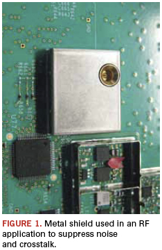
Also, in an RF application, signals generate parasitic coupling. The PCB layout engineer must implement ground shields or floods at the right locations in the layout to reduce parasitic coupling (Figure 1). Improving trace-to-trace impedance control is achieved by inserting ground shields between signal lines. This improves a uniform copper density across the entire board to ensure etch characteristics are equal to all signal lines. Again, if that’s not properly performed, test results send the layout back to the design for another go around.
Those are a few examples of what the savvy PCB layout engineer must know to successfully prepare a layout to achieve high-test coverage. Further, it’s important they fully understand the significance of such test procedures and characteristics as smoke test, gain and frequency response test, analog signature analysis (ASA), propagation velocity test, probing techniques, launch edge versus reflection edge, filtered TDR option, and others.
The smoke test is conducted to ascertain that data or signal aspects of the board are properly functioning. There are differences between a smoke test for digital and analog components. A smoke test provides some necessary assurances that system-under-test will not catastrophically fail. In other words, the circuit will not burn or systems will not crash. An example of the smoke test is the gain and frequency response testing. This involves measuring resistive points or loads between two different points to ensure they are balanced. The PCB layout engineer must understand this test because it helps prevent the circuit from burning, or at least avoids big mistakes from happening.
ASA monitors jitter, which occurs in digital ICs where the solid state jumps between two or three different points, thus causing instability. The experienced layout engineer will ensure a propagation delay between those two traces in order to make a stable state for doing ASA analysis, to control the jitter, and to ensure it’s within allowable parameters.
Propagation velocity testing involves propagation delay measurement and impedance measuring. Controlling impedance is relatively easy, and performing calculations and controlling a few factors to achieve impedance control is not difficult. But measuring propagation delay is considerably more difficult. Accuracy is extremely dependent on probing techniques dealing with connecting and terminating leads. Among the ones the PCB layout engineer needs to know about are handheld devices, SMA connectors, and controlled impedance micro probes, so they can factor in these test tools and considerations during layout.
As for launch edge versus reflection edge, the PCB layout engineer should have a firm understanding of this characteristic when doing high-speed designs. Last, filtered time domain reflects (TDR) option is used when excessive ringing occurs on a TDR response. Rise and fall edges must be aligned so they have zero time delay between rise and fall. Having this knowledge, the layout engineer is able to design the circuitry that is stable and has no jitters.
Sidebar:
Key ICT Guidelines
- Don’t tie IC control lines directly to power or ground. Add pull-up or pull-down resistors. This permits the ICT to control these lines when required during IC testing.
- Place test points away from BGA components to reduce BGA solder stress and board flex.
- Have a test point for all electrical nodes, including unused IC pins. This allows detection of internal and external shorts.
- To measure a low ohm resistor, two test points on each side of the component may be required to support 4-wire Kelvin resistance measuring.
- Oscillator should be gated with logic circuit, allowing ICT to disable the clock signal as needed during IC testing.
- Use boundary-scan-compliant devices when possible. This provides accessibility to the devices for boards with limited access test points. Also, chain multiple JTAG devices.
- If possible, place test points for each node on one side of the board (secondary side preferred). This reduces the fixture and maintenance cost. Top-side probing is less accurate than bottom-side probing.
Zulki Khan is founder and president of NexLogic Technologies (nexlogic.com); zulki@nexlogic.com.
A review of best-in-class controls for maintaining factory worker health.
The National Institute for Occupational Safety and Health (NIOSH) received a confidential employee request for a Health Hazard Evaluation (HHE) at an electronics manufacturer specializing in printed circuit board fabrication, assembly, and testing for different end-user applications (sidebar). At the time of our evaluation, approximately 2,300 employees worked at the facility in either the medical section plant or the defense and aerospace section. Employees were primarily concerned about exposure to solder paste and fumes, as well as dust and noise. They reported coughs, burning eyes, nosebleeds, voice loss, headaches, sinus infections, bronchitis, and respiratory problems.
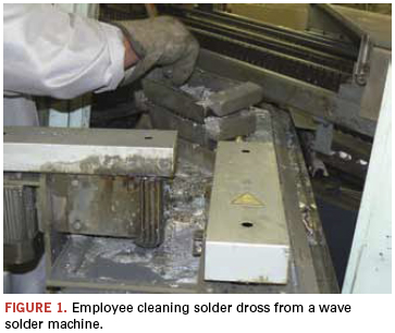
At the time of our evaluation, the medical section had four wave soldering lines and eight surface mount lines. Wave solder lines 1, 2, and 3 used Pb-free solder (96.5% tin), and wave solder line 4 used solder composed of 63% tin and 37% lead. The defense and aerospace section had five wave solder lines and six surface mount lines. It also had ruggedization, conformal coating and bonding operations, where the finished PCBs are fitted with additional structural supports and hand-brushed or sprayed with an acrylic copolymer to provide increased environmental and mechanical protection. Spraying during conformal coating was conducted in a ventilated, open-face, bench-top spray booth. Employees wore safety glasses and air-purifying, elastomeric, half facepiece respirators with organic vapor cartridges while spraying. At least once per shift, wave solder operators clean solder dross by using a ladle to remove dross floating on top of the molten solder (Figure 1). Residual molten solder inadvertently collected during this operation is separated with a sieve, and the remaining dross disposed of in a drum sealed with a lid. Employees are required to wear heat-resistant gloves over disposable nitrile gloves, a face shield, and an apron when performing dross cleaning. In addition to dross cleaning, employees periodically clean and maintain the wave solder machines. Finally, the facility has an auto insertion (AI) operation, which involves machine insertion of components onto a PCB by punching through it.
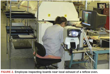
Assessment. During our first visit to the facility, we conducted confidential medical interviews with 40 employees, observed work processes and practices, collected general area air samples for volatile organic compounds (VOCs), and collected surface wipe samples for lead and tin. We also reviewed air sampling records, the respiratory protection program, injury and illness records, and material safety data sheets. After sharing our findings with employee and management representatives in an interim letter, we returned to the facility to collect personal breathing zone and general area air samples for lead and specific VOCs. We also measured noise levels at the AI stations, evaluated room acoustics near the air rotation units (ARUs), collected hand wipe samples to assess lead contamination on skin, and evaluated the effectiveness of the local exhaust hoods for the wave solder and surface mount machines (Figure 2).
Occupational exposure limits. NIOSH investigators use both mandatory (legally enforceable) and recommended occupational exposure limits (OELs) for chemical, physical, and biological agents as a guide for making recommendations. OELs have been developed by Federal agencies and safety and health organizations to prevent the occurrence of adverse health effects from workplace exposures. They suggest levels of exposure to which most employees may be exposed up to 10 hr. per day, 40 hr. per week for a working lifetime without experiencing adverse health effects. However, a small percentage of employees may still experience health effects due to personal susceptibility, a preexisting medical condition, and/or hypersensitivity (allergy). In addition, some hazardous substances may act in combination with other workplace exposures, the environment, or with medications or personal habits of the employee to produce health effects, even if occupational exposures are controlled at the level set by the exposure limit. Also, some substances can be absorbed by direct contact with the skin and mucous membranes in addition to being inhaled, which contributes to the individual’s overall exposure.
Results and Discussion
One of six personal breathing zone air samples for lead exceeded the Occupational Safety and Health Administration action limit (OSHA AL) of 30 micrograms per cubic meter (µg/m3) and was close to the OSHA permissible exposure limit of 50 µg/m3. This employee, a wave solder operator in the DAS, was cleaning the wave solder machines without wearing a respirator. The employee was exposed to an airborne lead concentration of 49 µg/m3. However, with this one exception, wave solder operators had lead exposures well below the OSHA AL.
Our surface sampling showed the presence of lead and tin on work surfaces in both sections of the plant. Currently, there are no OELs for surface metal contamination in occupational settings. We also sampled tables in two of the break rooms and found detectable levels of lead and tin in one of the break rooms. This suggests that workplace contamination is being tracked into the break rooms by employees’ footwear, clothing or hands, and that these areas should be kept cleaner.
Additionally, despite hand washing prior to sample collection, three of seven hand wipe samples tested positive for lead.
Full-shift noise exposures for the AI operators in the medical and defense and aerospace section were well below the NIOSH recommended exposure limit. Because telephone communication is not required in the production areas, and communication between employees is minimal, the louder noise levels experienced by employees with work stations near the ARUs were within the criteria specified by the balanced noise criteria (NCB) 55-70 curves. The NCB curves are a set of noise criteria for occupied interior spaces, devised to limit noise to levels at which speech can be reasonably understood. Refer to “Resources and Links” for more information on the NCB curves, as well as Appendix B of the HHE report (referenced in this section).
Our ventilation evaluation revealed that several local exhaust hoods were not effectively capturing process emissions. These included three hoods in the medical section and two hoods in the defense and aerospace section. This could have been due to local exhaust ventilation systems being imbalanced or improperly maintained. Air sampling results for specific VOCs indicated that employee exposures were well below all applicable OELs.
Although both the medical and defense and aerospace section share the main workspace and have similar tasks and equipment, the health concerns originated exclusively from employees in the medical section. Of the 40 medical section employees we interviewed, 23 did not report any work-related symptoms. The most commonly reported symptoms were upper respiratory, including runny nose, cough, and sinusitis; fatigue (frequently related to overtime work), and voice loss. However, these symptoms are also common in the general population, and we could not attribute them to the exposures documented.
Last, we found inconsistencies between the facility’s written respiratory protection program and employee practice. The written respiratory protection program required respirators to be worn when cleaning wave solder machines. However, it did not identify the appropriate type of respirator that should be worn for this task, and we did not observe employees wearing respirators when performing this activity. In addition, employees were voluntarily wearing respirators during spraying in the conformal coating area.
Recommendations
We made a number of recommendations to the facility to improve employee health and safety. Many of these recommendations may also apply to readers’ facilities:
- Use engineering controls such as portable exhaust hoods when removing solder dross and cleaning wave solder machines. Periodically evaluate the local exhaust hoods to ensure they are performing per manufacturer’s specifications. Evaluate their effectiveness at least every three months, and within five days of a production, process, or control change.
- Comply with all requirements of the OSHA lead standard (29 CFR 1910.1025). This includes instituting an industrial hygiene monitoring program to assess lead exposure for employees working with leaded solder, or for employees having the greatest potential for lead exposure. Additionally, institute a maintenance program for evaluating enclosed local exhaust hoods used to control lead exposure.
- Improve general housekeeping practices to ensure break rooms and work surfaces are clean. Use commercial cleaning wipes that are made for removing lead and other heavy metals every shift to keep work surfaces such as control consoles clean. Use high-efficiency particulate air vacuum cleaners in work areas to minimize dust in the air.
- Practice good personal hygiene. Thoroughly wash hands before eating, before and after using the restroom, and before leaving work. Eating, drinking, smoking, and applying cosmetics in work areas should be prohibited.
- Ensure that the respiratory protection program meets all applicable requirements of the OSHA Respiratory Standard (29 CFR 1910.134). The written respiratory protection program should identify job tasks requiring a respirator to be worn, the type of respirator needed, and the locations where respirator use is required. Evaluate respiratory hazards for job tasks currently requiring respiratory protection to ensure protection is adequate. The program should also note any job tasks for which employees voluntarily wear respirators.
- Encourage employees to report work-related health concerns. Consult a physician trained in occupational medicine (see “Resources and Links”).
- Train employees about potential exposures and how to protect themselves from hazards, and promptly communicate any health and safety changes to employees.
Sidebar:
The Health Hazard Evaluation Program
Based on a federal law, NIOSH conducts Health Hazard Evaluations (HHE) to investigate possible workplace health hazards. Employees, employers or union representatives can ask our comprehensive team of experts to investigate their health and safety concerns by requesting an HHE. Our team contacts the requestor and discusses the problems and how to solve them. This may result in sending the requestor information, referring the requestor to a more appropriate agency, or making a site visit, which may include environmental sampling and medical testing. If we make a site visit, we prepare a report of our investigation that includes recommendations specific to the problems found, as well as general guidance for following good occupational health practices. HHE reports are available on the Internet (http://www.cdc.gov/niosh/hhe/).
Resources and Links
1. NIOSH HHE program information, cdc.gov/niosh/hhe/HHEprogram.html.
2. Link to this HHE report: cdc.gov/niosh/hhe/reports/pdfs/2007-0201-3086.pdf.
3. Code of Federal Regulations (CFR), 29 CFR 1910.95, US Government Printing Office, Office of the Federal Register.
4. L.L. Beranek, “Criteria for Noise and Vibration in Communities, Buildings, and Vehicles,” Noise and Vibration Control, Rev. ed. Cambridge, MA: Institute of Noise Control Engineering; 1988:554-623.
5. L.L. Beranek, “Balanced Noise Criterion (NCB) Curves,” J Acoust Soc Am., 1989; 86(2):650-664.
6. Acoustical Society of America, ANSI S12.2-1995, “Criteria for Evaluating Room Noise,” 1995.
7. Association of Occupational and Environmental Clinics (aoec.org).
8. American College of Occupational and Environmental Medicine (acoem.org).
Srinivas Durgam was an industrial hygienist at NIOSH (cdc.gov/niosh) during the time of this evaluation; srinivasdurgam@hotmail.com. Chandran Achutan, Ph.D., is assistant professor at the University of Nebraska Medical Center (unmc.edu); cachutan@unmc.edu. Carlos Aristeguieta, M.D., was a NIOSH medical officer during the time of this evaluation; arcwor@gmail.com. Maureen Niemeier is a freelance technical writer; mtnrtn@fuse.net.
Testing parts for gaps reveals which parts are electrically intact but prone to future delamination.
In an ideal world, plastic-encapsulated microcircuits (PEMs) would leave the component manufacturer in pristine condition. BGAs, QFNs, PQFPs, TOs and other package types would have no electrical or structural anomalies that could lead to electrical failures. The components would arrive for assembly in this condition, and would pass through handling, reflow and testing with no alteration of their ideal state. They would give years of flawless service.
In the real world, things do not always work out like this. A component may pick up a gap-type structural anomaly – delaminations, voids and cracks are the common ones – somewhere between the molding process and post-assembly shipment. Many of these gap-type anomalies make no difference in the proper functioning or lifespan of the component. Some, though, depending on size and location within the package, can expand until they break a connection. Even without expanding, gaps are the locations where moisture tends to collect, whether it has percolated through the mold compound or entered by a crack along a lead finger. The combination of moisture and contaminants, which can arrive by the same routes, can promote corrosion that may lead to electrical failure.
The least dangerous gap-type PEM anomaly is probably a small void (air bubble) in the mold compound not near to or in contact with any other surface such as a wire or the die. Generally such an anomaly is not considered a defect. Far more dangerous are defects such as delamination between the mold compound and die face. Normal thermal cycling, with repeated coefficient of thermal expansion stresses, can cause the delamination to expand across the face of the die until it shears off a wire bond.
There are numerous other gap-type anomalies, and many pose a greater or lesser threat to electrical performance. The important questions during assembly are:
- What percentage of the components in a given lot has internal structural anomalies?
- How likely are these anomalies to cause eventual electrical failure?
Sonoscan’s applications laboratory, which images lots of components for assemblers, routinely uncovers the answers to both questions. The assembler that will use the components writes the rules that will distinguish harmless anomalies from dangerous defects. Acoustic micro imaging systems image and analyze internal gap-type features, which reflect ultrasound at higher amplitude than other internal features such as the die or lead fingers.
PEMs in which a gap-type feature has already broken a connection will, of course, fail electrical tests. The purpose of acoustic screening is to identify and remove those PEMs that are electrically intact, but that have gap-type defects likely to cause field failures. For commercial products, defects of a certain size may be acceptable if the risk of failure is low. In military, aerospace and medical products, the degree of risk permitted ranges from very low to zero.
The outcome of acoustic screening varies greatly from one lot of components to another. It is not uncommon for a lot of components to have up to 5% rejects. The accept/reject criteria are defined by the user of the part and are applied to internal anomalies visible in the acoustic images.
Acoustic images reveal all sorts of anomalous situations. The ultrasound pulsed into a component is reflected from material interfaces at many depths, but the echoes can be selected by their arrival time to limit the acoustic image to a desired depth. The acoustic image of the BGA in Figure 1 captured the depth from just below the top surface of the mold compound to just above the die, and included the tops of the wires (at center). The red and yellow features are voids in the mold compound. Such isolated voids are generally considered harmless. But this BGA has a great many voids, running down to sizes so small that they get lost in the tiny white features created by the distribution of particles in the mold compound.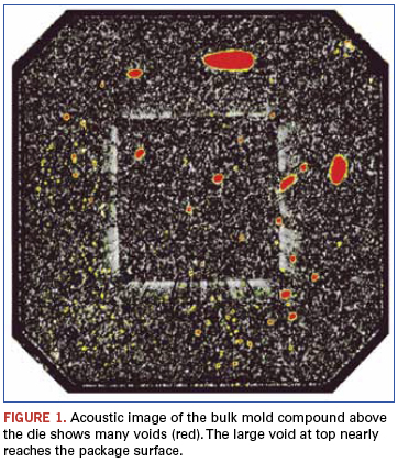
But by using a new technique to image the bulk of the mold compound in many sequential slices, the Sonoscan lab found the real danger: The largest void, at top, extends vertically from the substrate upward almost to the top surface. Moisture and contaminants that percolate through its thin wall have a free ride to the center of the package.
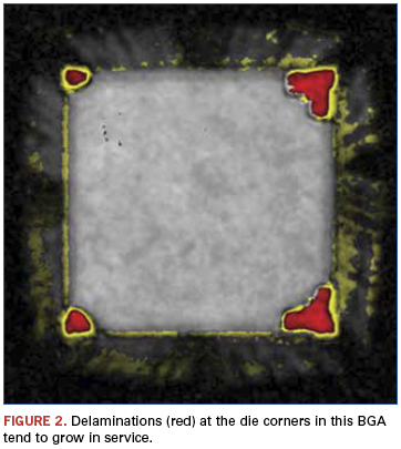
Figure 2 is the acoustic image of the die surface in a BGA that would almost certainly pass electrical tests, but that is loaded with potential disaster. The red areas at each corner of the die face are small delaminations of the mold compound from the die. At this early stage, the delaminations are unlikely to have yet broken a wire bond on the die. The normal thermal cycling of service, however, is what makes die face delaminations so perilous; they may expand laterally until they find and break a wire bond.
A PEM that is being tested in a laboratory that determines Moisture Sensitivity Level (MSL) is initially dried to remove existing moisture, then moisturized to a specific level. It next goes through reflow three times, although it is not soldered to the board, since it will later be sectioned physically. The three passes through reflow simulate the experience of a component on a board that is reflowed twice and is then reworked. After the third reflow, the PEM undergoes a basic electrical test to find opens. It is then screened acoustically to look for gap-type defects, and then physically sectioned to see the defects optically. The acoustic image is the guide for selecting the best location for physical sectioning. Some defects, though dangerous, cannot be seen after physical sectioning because they are too thin. Delaminations as thin as 1 µm reflect virtually all of the ultrasound and are imaged strongly, but such a thin gap may be invisible optically.
MSL test personnel often encounter a PEM whose acoustic image shows multiple problems – voids, delaminations, even cracks – but which passed the electrical tests. Such a PEM may be loaded with structural anomalies that will cause electrical failure under the stress of service, but none of those anomalies happens to have caused a problem yet. In a production environment, such a “train wreck” can sail through basic electrical testing and go right into production.
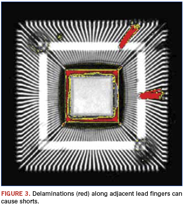
Figure 3 is an acoustic image of a high-risk PEM. It has two types of defects. First, the die paddle is delaminated (red) from the mold compound around the periphery of the die. This is a moderately serious condition; the delamination could expand and move under the die and the die attach material. But in two locations on the lead fingers is another dangerous condition: delaminations on adjacent lead fingers. The wall of mold compound between the lead fingers is very thin, and can easily be dissolved by corrosion, causing a short between the lead fingers.
The same result – a short between adjacent lead fingers – can be triggered by a different mechanism often encountered in Sonoscan’s laboratories. In some PEMs, the tape (white in Figure 2) looks red or yellow in the acoustic image because it is delaminated from the mold compound. Although frequently considered unimportant, corrosion along such a delamination can also put two adjacent lead fingers in electrical contact.
The locations and types of gap-type defects are largely determined by the package design. Delamination of the mold compound from a lead finger, for example, may not even be considered a defect if a package has long lead fingers on which there are a few small delaminations. They are unlikely ever to grow sufficiently to like the outside atmosphere and the die or the wire bonds. But a package design having a very small die and very long wires connected to very short lead fingers is a different story. The distance from the outside atmosphere to the outer wire bonds is very short, and can be bridged even by a small delamination. The very long wires are also vulnerable to wire sweep during molding.
One of the defects MSL test personnel expect to see in some PEMs is the popcorn crack. Popcorn cracks form when moisture within the package turns to steam during reflow and expands in volume by about 1600 times. Popcorn cracks are not as frequent in production as they were a decade or two ago, but they still occur. They usually originate at the die attach level and travel downward to the bottom surface of the package. Very few travel to the top surface, and even fewer go sideways. A popcorn crack exiting the bottom of the package is invisible during production, but over the life of the components provides a convenient path for moisture and contaminants to reach the die.
Acoustic screening uncovers all sorts of things. Die face delaminations have a reputation for being lethal, but there are a very few specific packages in which, users
have found, small die face delaminations practically never cause electrical failure, probably because of a lucky combination of design and materials. Acoustic screening lets the user check the initial state of these delaminations. Another user might find that a lot of familiar PEMs suddenly shows numerous, large delaminations in a large percentage of components. These may be counterfeit PEMs, starting on their second lifetime of service. Or the defects may simply result from a change in mold compound or fabrication processes.
The most dramatic outcome of acoustic screening is the avoidance of mass field failures. In less dramatic scenarios, the weeding out of problem components gives a boost to overall product reliability.
Tom Adams is a consultant at Sonoscan Inc. (sonoscan.com); tom100adams@comcast.net.

Press Releases
- Javad EMS Upgrades Through-Hole Soldering Capacity with New SEHO PowerWave System
- Sharpen Your Selective Soldering Skills with Kurtz Ersa's July VERSAFLOW 4/55 Training
- Omron Advances Inspection Technology with NVIDIA Omniverse and Metropolis
- Seika Machinery’s SMI 2026 Webinar Series Continues with Focus on PCB Cleaning Before Solder Paste Printing