

Formed just a decade ago, our EMS Company of the Year, AsteelFlash, is moving as fast as its name.
Foxconn’s topline growth may make it the envy of any manufacturing company, but under the radar, at least one Tier 2 EMS firm has been expanding almost as quickly.
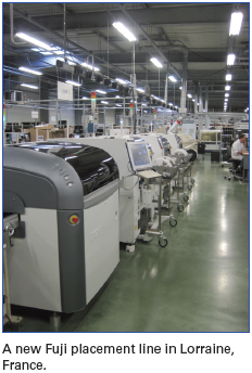
Since its inception as Asteel in 1999, the company has rapidly grown both organically and by acquisition, boosted in large part by its February 2008 purchase of Flash Electronics. The merged entity now encompasses 12 production sites on four continents, and ranks third in size behind only Elcoteq and Zollner (founded 1965) among Europe-based EMS companies.
On its own, Asteel was growing steadily, topping $200 million in revenue in 2007. But it was the acquisition of Fremont, CA-based Flash Electronics that shot the company up the EMS charts. The combined entity – Asteel also purchased UK-based MRP Electronics that year – boosted Asteel from primarily a central European player to a legitimate worldwide entity. It is the only Tier 2 (revenues between $500 million and $1 billion) to see sales double over the past decade. Yet through the rapid change in size and geographic scope, Asteel’s management, manufacturing approach and corporate philosophy have remained constant.
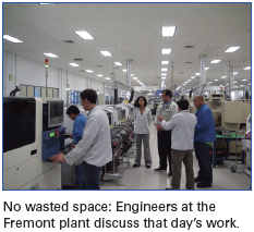
Gilles Benhamou has been there from the beginning. Starting in 2000 with a greenfield, the founder and chief executive says the model has been to build in small batches close to customers and to the point of end-use, and to focus on industrial and related technologies, while staying away from lower-margin products like cellphones. Networking infrastructure, storage, industrial, RF, and lighting are the primary end-products. “We want to produce on each continent for its domestic market. We build very complex product in small batches. We can do boards with 16,000 components, but the average [lot size] is 25 pieces.” Today, high-mix, low-volume orders make up 60% to 70% of revenue, and 200 pieces would be considered a large batch.
Because each of the 12 production sites has similar core competencies, they follow the same strategy. Lean manufacturing and design rules are uniform across the company. Quality documentation also is instituted globally.
Beyond the equipment and manufacturing practices, management takes great care to ensure a common culture – no easy feat given the inherent regional differences. Still, Benhamou sees a unified company as a must. “We are different,” he acknowledges. “All our management and worldwide team must know each other and work together. We only want one culture in AsteelFlash, and it’s very important, or one day you could have a problem.”
This is how a global company can ensure consistent customer service across dozens of time zones and an even greater number of national or ethnic divides. “We have people everywhere able to work a lot, on Saturday and Sunday to satisfy the customer. But when you have the culture, it’s no problem. It’s our job; it takes a lot of energy. The main point is we constitute one group, and to hire the right people to support that customer.”
The cultural philosophy informs AsteelFlash’s site locations. “At the NPI, it’s very important to be near the end-customer. You want on-time delivery. You cannot do that if all the design development team is not very close and cannot react to tests and so on. It’s very important to localize parts.”
One differentiator is the company’s commitment to Northern Africa. Although AsteelFlash is not the only EMS player there, it is easily the largest both in terms of factory space and revenues. The company’s third factory in Tunisia is scheduled to come online by mid 2011 and will double the contract electronics manufacturer’s capacity there to 390,000 sq. ft. Forecasts call for AsteelFlash to double its revenue this year and next in Tunisia, as customers move programs west from China. The company also plans to add 1,500 workers, for a total of 2,500 by 2014.
“It’s very important to be close to our customers as an NPI and ODM, to be able to meet them and make recommendations for the global supply chain and procurement,” Benhamou says. “Tunisia is a long-term, low-cost center. Wages are controlled under long-term policy. When you see what has happened in China with labor [where steep wage inflation has taken place over the past year], it’s not at all the same in Tunisia. The evolution of wages is progressively controlled.”
Tunisia also fits the company’s desire to be close to its customers. The nation is one hour by air to Milan and two to Paris. “If you have problems, you can be there in the same day. It is very flexible,” says Benhamou. The proximity compresses the supply chain both in Europe and in the US to four to five days, he adds, versus the 10 to 15 days it could take to deliver to the eastern US from China.
AsteelFlash sees as its sweet spot customers of modest to medium size, but with high-mix products. “We are able to produce for companies with $10 million to $20 million in revenue. They cannot have this same type of service with Tier 1s. Tier 1s want to focus on big business.
“We can support a customer in a global view, but we are not too huge. We can take a project with three factories together – Europe, Asia, US – and work with only one team in front of the customer. We could commit, for example, to customers that the ramp will be done in France, but local content will be built in the US.”
There aren’t many EMS companies that can offer this combination of size and breadth, Benhamou asserts, and he’s right. According to the Circuits Assembly Top 50, 12 EMS companies had annual revenues between $400 million and $1 billion last year. Of them, only Kimball also has sites in the three major regions. And none can boast AsteelFlash’s balance: In terms of revenue, China makes up 35%, the US contributes 25%, and Europe 40%.
AsteelFlash sees further expansion ahead. The company alludes to possible acquisitions in Mexico and on the East Coast in the US, in addition to other countries in Europe. It also sees growth in military and aerospace and medical, which currently are not major end-markets it serves. “We want to develop our footprint in Europe and the US. We want low-cost centers in Tunisia and Mexico, places where added-value can be done,” Benhamou says. Internal forecasts call for revenues to reach $850 million next year and $1 billion in two years.
For its thoughtful management and consistent approach, its topline growth over a decade’s time, and its willingness to pioneer fresh locales, AsteelFlash is CIRCUITS ASSEMBLY'S 2010 EMS Company of the Year.

Others of Note
Here are some other EMS companies that, for better or worse, made a mark in 2010.
Flextronics: Who says an American company can’t excel in PC manufacturing?
Foxconn: Internal personnel crises (not to mention the ever-increasing revenue spike) precipitate a massive shift inland.
IEC Electronics: Small tier EMS firm is one of the great turnaround stories of the past decade.
Lightspeed Manufacturing: EMS veteran Rich Breault continues to show that success isn’t necessarily
tied to size.
Mike Buetow is editor-in-chief of CIRCUITS ASSEMBLY; mbuetow@upmediagroup.com.

Lower-concentration cleaning agents are one response to “green” demands.
Writing this column is a tremendous opportunity to comment on the rapidly changing world of precision cleaning within electronics. In short, cleaning is becoming more difficult and more demanding. It is our job to meet these new challenges head on and translate them into opportunities. So, what is changing, you might ask?
For one, the increasing local and global (i.e., RoHS, UNEP, GHS, etc.) initiatives to become “greener” have customers requesting more environmentally sound process solutions. At the same time, the need to clean better under low-standoff components has arisen. And, if that is not enough, customers expect more engineering support to identify additional improvements to their cleaning process, leading to a lower cost per cleaned part.
While we all understand and embrace efforts to provide our children with a safer and healthier world, we cannot easily ignore the effects of the global recession. At first glance, it seems that this calls for some tough choices. How can we continue to produce high-reliability products on a tighter budget, while implementing new and green technologies? Often, innovations as well as cost savings require upfront investment. It is here where we have to educate our customers about the solutions they might not be even aware of.
Let’s take a few prime examples to illustrate the possibilities of making a cleaning process greener:
- Lower, yet stable, operating concentrations to minimize chemistry consumption.
- Elimination or reduction of volatile organic compounds (VOC).
- Cleaning agents with lower pH levels to reduce effluent operating costs.
Operating chemistry concentrations is one topic I have addressed in various previous columns. Greener cleaning processes can be achieved through lower and more stable concentrations that in turn help minimize chemistry consumption. One obvious fact: The higher the concentration, the higher the user cost. Factors such as the bath life of the cleaning agent also have to be taken into account. Assuming the same bath life, a lower concentration leads to direct savings, which is exactly what the latest cleaning agent technologies provide, as they can be used at 10% or less. It is also important to point out, however, that actual and perceived concentration can be two entirely different values. Once the operator begins to use the cleaning agent, the dissolved contamination affects the concentration measurement. Thus, overconcentration through ineffective measuring techniques can cost you handsomely. New bath analyzing technologies have emerged to help users accurately maintain concentrations. So, please, check your process, as this could lead to significant savings.
Second, VOCs are integral parts of many cleaning agents and serve a very important purpose. They support the cleaning agent’s job by solubilizing organic contamination. Reducing VOCs generated by cleaning processes, however, is a worthwhile thought because it would minimize their environmental effects. However, if one were to simply eliminate VOCs from the cleaning agent, it would have detrimental effects on the cleaning results, and product reliability would be everyone’s buzzword. On the other hand, numerous avenues do exist to control the environmental impact of cleaning agents containing VOCs. Most notable are vapor recovery techniques with efficiency rates between 15% and 85%.
This type of investment in process improvements also can help minimize cost. Appropriate vapor recovery techniques such as “condensation” (through active cooling) not only help maximize the collection of chemistry, but also recover DI water. Both are subsequently returned to the wash tank and recycled in the process, leading to substantial cost savings and a minimal impact on the environment.
Third, pH-neutral products for defluxing and stencil cleaning have emerged and are undergoing test and implementation. Similar to vapor recovery, the use of pH-neutral products enables users to benefit from more environmentally sound process solutions at an overall lower price. Users can now directly dispose effluent water from the chemical isolation section (sometimes 5 gal./min.) without extensive wastewater treatment. Given an acceptable cleaning performance, these new innovations combine environmental benefits with process savings: a win-win situation for vendor and customer.
We should set goals for ourselves to work toward. Accepting the status quo or waiting for someone else to innovate does not exemplify leadership, nor does it show responsibility for tomorrow’s world. So, how low can you go?
Ed.: Those concerned about environmental regulations should read Kal Kawar each week at circuitsassembly.com/blog.
Harald Wack, Ph.D., is president of Zestron (zestron.com); h.wack@zestronusa.com.

As influential as EMS and ODMs have become, the customer still drives the ship.
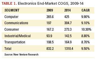
Those who follow our research know that we keep a close watch on the worldwide OEM electronics manufacturing market: in other words, the computer, communications, consumer, industrial/medical and transportation sectors. It is an enormous market in terms of revenue, reaching nearly $1 trillion in cost of goods sold (COGS) in 2008, before slipping to $832 billion in 2009. The recovery is expected to exceed $1.3 trillion by 2014 (Table 1).
What is remarkable about this market is its robustness. It is difficult to find markets of this scale expanding at the current compounded growth rate. Even more amazing, this growth rate has increased over the past few years with the explosion of notebook computer and mobile phones. Over the next five years, taking the lead will be consumer products: flat and 3D TVs, video game consoles, navigation systems and IP set-top boxes.
By comparison, the medical market always has exhibited solid growth, mainly in the areas of diagnostics and imaging systems, as well as surgical and monitoring equipment. Until last year, industrial product industries such as semiconductor capital equipment, process control, test and measurement steadily expanded. Yet with the downturn in 2009, capital spending went into a deep freeze and these markets contracted considerably. The same was true for automotive, although aerospace/defense and “other transportation” (off-road, trains, marine, etc.) remained relatively strong.
Nearly two-thirds of the OEM market today is comprised of computer and communications equipment, and this percentage is growing. A large part of these markets is commodity in nature, and once OEMs engage in the Asian business model of margin depletion, little money will be made from these sectors. Oddly, ODMs – e.g., Compal, Asus, Quanta, Wistron – (discussed later) last year were some of the most profitable in the industry. While EMS companies collectively lost $7 billion, ODM firms made more than $2 billion.
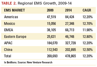
The real story behind the growth of the OEM market lies in where the assembly of electronics products is taking place. In this regard, we must look to EMS suppliers (including ODMs) and the growth rates associated with production taking place in low-cost countries. Today, EMS assembly accounts for around 32% of the total electronics assembly market. Yet, the growth of these suppliers in the three general low-cost regions (Mexico, Eastern Europe and China) account for the highest growth rates. Assembly value in these regions is approximately 50% higher than in high-cost regions (Table 2).
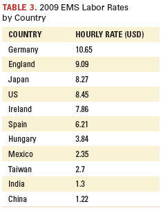
The reason behind this disruption can be understood when comparing the average base (unburdened) labor rates throughout the world. Essentially, an order of magnitude of difference exists between low-cost regions when compared to the base wage rate of high-cost regions. Making matters more difficult, once a competitor makes the move to migrate to a low-cost region, frequently others must follow to remain viable. (As the saying goes, “Once one cow crosses the rivers, so will the others.”)
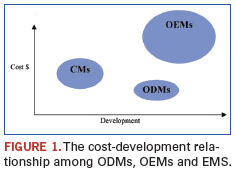
ODMs have disrupted the EMS industry the way EMS suppliers once disrupted the OEM electronics industry. ODMs typically have a lower cost of operation due to their focus on a select few commodity products and Asian (read: low cost) operations base. Moreover, they can discount assembly prices by raising design and component prices, which are often bundled into their service offering. As a result, EMS suppliers find it difficult to compete head-on with ODMs in the product sectors they excel in. Figure 1 highlights the supplier differences in value-add and cost.
OEMs like to work with ODMs because they lower risk by not having to invest in design, materials or inventory. (EMS companies frequently burden the OEM customer with inventory liability.) ODMs are attractive because they offer advanced designs, fresh IP and the ability to bring a new product to market very quickly. Where ODMs add risk is they may become a competitor once they gain the product design knowledge, as has happened in the past. Moreover, ODMs have a tendency to tolerate unhealthy profit margins just to gain a contract, and this can be risky for the OEM should the market soften or they go out of business. (Oddly Foxconn, officially an EMS company, succeeds by modeling an ODM business.)
With the EMS industry only accounting for 32% of the total available market, one might ask where is the other 68% of OEMs’ product assembly? The answer can be found in the geography and business philosophy of leading electronics companies. By a wide margin, Asian (Chinese, Taiwanese, Korean and Japanese) OEMs prefer to manufacture in-house, while North American and increasingly European OEMs are looking to outsource as their business model. Further, a high percentage of OEM products simply are not able to be outsourced (aerospace, defense, medical, industrial, etc.) and are often produced in such low volumes that subcontracting is not profitable. As a result, EMS penetration is not expected to exceed more than 37% of the entire OEM industry by 2014.
NVR has analyzed the opportunity for outsourcing by market industry and leading OEM company in excruciating detail through its recent report, The Worldwide OEM Electronics Assembly Market – A Unique Database Providing Global Electronics Assembly Data on Nearly 300 of the World’s Leading Outsourcing Companies, published in August 2010. For more information, see newventureresearch.com.
Randall Sherman is president and CEO of New Venture Research Corp. (newventureresearch.com); rsherman@newventureresearch.com. His column runs bimonthly.
Procedures for preventing and ridding moisture from components.
As packages get smaller, the risk for damage to moisture-sensitive devices increases. With the higher temperatures required for Pb-free soldering, that risk is further compounded.1 That’s why it’s extremely important to be aware and vigilant of MSDs.
ICs can act like a sponge. If they have semi-permeable membranes, moisture from the ambient air can get into those devices. When they get rapidly heated during reflow or rework, the result is rapid outgassing. In some cases, this excessive outgassing causes popcorning, which can damage the internal structures of a component.2
To minimize and eliminate the adverse effects related to MSD, assembly personnel, process engineers and technicians must diligently apply regimented practices based on the IPC/JEDEC J-STD-033B.1 standard. This standard sets out a long list of procedures that must be implemented for handling, packaging, and shipping MSDs.3
Protecting and controlling MSDs on the assembly floor takes into account a great number of large and small procedures and important steps. Violating, ignoring or overlooking any or a series of these precautions could result either in costly rework or latent PCB defects.
More often than not, electrical test catches the popcorning problem in an MSD. But in this instance, damage may not immediately lead to a failure and instead present itself as a latent defect. Subsequently, such a component compromises a finished PCB and can lead to system failure in the field. Therefore, trained process engineering personnel, experience, and a highly disciplined and structured assembly operation are critical to protect surface mount components from humidity present in an assembly environment.
Affected components can include any surface mount devices, ICs and discrete devices that mount to one surface of a PCB when assembled.3 MSD components are specified by their respective manufacturers to have a limited floor life at or below 30°C or 86°F and 60% relative humidity (RH).3
Tools of the Trade
Four materials and techniques help protect and control MSDs. Those are moisture barrier bags (MBB), desiccant, humidity indicator cards (HIC), and moisture-sensitive caution labels. Storing MSDs in MBBs provides the first line of protection and restricts transmission of water vapor. Desiccants further boost MSD control when used to absorb moisture that gets into the MBB or is sealed in it. It’s also advisable to include more desiccant to absorb moisture in component carrier materials such as trays, tubes and reels.
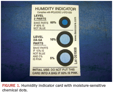
The HIC does its part with its moisture-sensitive chemical dots (Figure 1). Those dots change color from blue to pink when indicated RH is exceeded inside the MBB. The card must have a 5, 10, and 60% RH sensitive dot. The HIC has instructions for when to bake parts, depending on the moisture sensitivity level (MSL) of a particular device. For example, if a device has an MSL of 2, then the parts need to be baked if the 60% dot is not blue.3 For devices of MSL level 2A-5A, then parts need to be baked if the 10% dot is not blue and the 5% dot is pink.3
MSL is the classification of the MSD’s floor life for the Pb-free condition or SnPb soldering condition at the factory ambient environment (≤30°C/60% RH). The MSL for Pb-free processes is higher than the MSD for SnPb process for the same component. The higher MSL has a shorter floor life than the lower MSL. Floor life means the out-of-bag life, not including the life in the safe storage. Therefore, for the specific reflow process, the proper MSL must be chosen. Misusing SnPb MSL for the Pb-free reflow process results in MSD damage from moisture absorption and yield/reliability degradation that can affect products in the field.
Most moisture-sensitive components are MSL 3 for SnPb soldering and MSL 4 for Pb-free soldering. For example, a moisture-sensitive BGA component has two MSL markings on its MS label: MSL 3 for SnPb process and MSL 4 for Pb-free process. This means that it has 168 hr. of exposure time to factory ambient environment if used in SnPb reflow, or 72 hr. of exposure time if used in Pb-free reflow.3 Compared to the traditional SnPb reflow process, its Pb-free process air exposure time is reduced 57%. Special attention must be paid to tight floor life management for RoHS projects.
Some MSD packages have multiple MSL markings: 2/240 and 3/260. This means that for SnPb reflow (peak temperature of 240°C), an MSD can be treated as level 2 MSD. For Pb-free reflow (peak temperature of 260°C), this MSD should be treated as level 3 MSD with shorter air exposed time (floor life).
At the outset, it is the responsibility of the assembler to require all suppliers and customers to follow J-STD-033B.1. The assembler must be sufficiently vigilant of suppliers’ and even customers’ poorly packaged and shipped MSDs that violate the standard. It’s also the assembler’s duty to keep suppliers and customers accountable for maintaining procedures in accordance with J-STD-033B.1.
An assembler’s receiving and stockroom has its own agenda for controlling MSDs, as well as strictly following J-STD-033B.1. Foremost is creating and maintaining an MSD control event logbook to record specific problems and solutions on given dates, and verify such information with an inspector’s signature. Incoming QC inspectors check whether the 5% dot is pink. These personnel should also inspect and, when necessary, reject damaged dry pack components, unsealed dry packs, missing desiccant or HIC dry packs. An operator must copy the MS level and floor life to new MBB labels when transferring MSD components to a new MBB.
From a general MSD environmental control perspective, the assembler must install digital temperature and RH meters in the stockroom and SMT production areas. MSD handlers read in real time data involving floor temperature, floor RH and the out-of-bag total time during the assembly process, and out-of-MBB environment. Based on that data, they implement MSD procedures and record MSD condition information. Meanwhile, production managers monitor factory ambient conditions. If room temperature exceeds 30°C (86°F) or room RH is more than 60%, floor life indicated on the MS label is no longer applicable and must be de-rated.
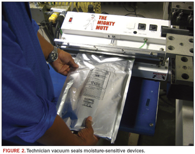
In keeping with the standard, it’s also important to be well stocked with certain items. Those include foam covers or bubble wrap for use around a stake of trays inside the MBB to avoid puncture during the sealing process. ESD-safe black card paper must be used to cover a tray’s bottom and top sides before it is inserted into an MBB. Moisture barrier bags and a vacuum-operated bag-sealing machine are vital as well (Figure 2). Special care must go toward using this machine, and the vacuum must be sufficiently relaxed to keep the tube or tray from puncturing the bag.
Baking Procedures
MSD control at the kitting stage involves three major steps. First, process engineering personnel must separate large quantities of MSD packages into small quantities based on the running batch size. Next, certain procedures are performed to properly receive all production-returned MSDs. All returned MSDs are to be resealed. Personnel ensure MBBs are identified with correct part number, quantity and MSD label. Last, manufacturing personnel properly arrange bake time to meet production requirements.
Another trio of steps is involved for production scheduling. First, for water-soluble-paste double-sided MSD boards, technicians finish both sides on the same day without washing between bottom and top reflow. Second, on the same day, they must finish all rework before sending the jobs to washing. One or two days before production, technicians arrange incoming QC of all MSDs. At the same time, they ensure there is sufficient time to bake those MSDs, keeping in mind that some MSD BGAs require 48-hr. baking. Third, technicians track MSD floor life and exposed time, as well as monitoring any noncompliant issues.
Meanwhile, in the SMT area, an SMT operator should record bag-opening date and time, as well as check and report to the floor manager any MSDs with longer floor life than that marked on the bag. Another procedure is to have SMT or other production and engineering groups return all remaining MSDs when their jobs are completed. Following that procedure, stockroom technicians re-seal all MSDs and record sealing data and time.
In some cases, assemblers will find it necessary at the kitting stage to bake MSDs before placing them on the production floor. If shelf life or RH on the HIC has been exceeded, components need to be baked until the moisture is removed. There are at least a half-dozen steps that must be carefully performed to bake components according to spec.
For example, it must be understood that baking degrades MSD solderability, thus causing quality problems.2 To avoid degrading solderability, a cumulative bake time limit of 48 hours at 125°C is imposed.3 However, floor personnel must be alert to the fact that MSD baking conditions depend on component body thickness and MS level.
Further, they are not to bake mixed MSDs with different body thicknesses in the same baking oven at the same time. Another similar procedure is “don’t bake mixed MSDs with different bake time at the same time in the same oven.” It is also a good practice to have separate baking ovens for PCBs and components and a detailed log maintaining all the records.
Each MSD can be baked only one time, and no second baking is allowed. Moreover, an MSD without clear MS Level marking on the package is not to be baked. Baking temperature is 125°C for 24 hr. with tolerance range for temperature control ±5˚C (120–130°C). Baking time should follow IPC J-STD-33B.1, Table 4-1.
Different MSD component trays/carriers have different maximum bake temperatures. It is vital always to check the tray bake temperature for each tray before sending it into the bake oven. Also, floor personnel should collect, recycle and store 140˚C or higher MSD trays with different sizes. Use them to replace the low bake temperature trays from suppliers or customers. A final procedure for any assembler to follow is if floor personnel don’t know the MSD baking history, it is time to stop MSD baking.
References
1. Thomas Ellison and James Szabo, “RoHS Implementation Challenges,” IPC/JEDEC 12th International Lead Free Conference, March 2006.
2. R.L. Shook and J.P. Goodelle, “Handling of Highly Moisture-Sensitive Components: An Analysis of Low-Humidity Containment and Baking Schedules,” ECTC, June 1999.
3. IPC/JEDEC J-STD-033B.1 - Includes Amendment 1, Handling, Packing, Shipping and Use of Moisture/Reflow Sensitive Surface Mount Devices, January 2007.
Don Shell is business development director at Nexlogic Technologies (nexlogic.com); info@nexlogic.com.
San Jose showed once again why it’s the epicenter for printed circuit design.
The outside temperature hit 103°F in the Silicon Valley, but inside the action at the PCB West trade show was even hotter.
Attendance at PCB West in late September was up markedly – 26% for the exhibition and 35% for the conference. Overall attendee registration jumped 20.4%, as the industry responded with vigor to the strong lineup of exhibitors, complemented by an outstanding technical program.
Signal integrity remained a major area of interest, although during the PCB Designers Roundtable – cosponsored by the good folks from the Silicon Valley Designers Council chapter – it was revealed that perhaps one-third of designers don’t actually perform SI analysis. (It’s left for someone else.) Proponents on hand, including the ubiquitous Rick Hartley, who taught several classes during the three-day technical conference, stressed that all designers should perform some level of SI. Also revealed: A large percentage of designers continue to manually route their boards, despite evidence showing autorouters could save time. Whether they do so because they are trying to protect their jobs is certainly understandable, but the notion that autorouting could free up resources that could then be used in other areas (such as SI analysis) bears consideration.
Many of the technical sessions that accompanied the trade show were packed, as designers and process engineers took advantage of the free sessions to glean valuable information on reducing layer counts, thermal management, post-assembly cleaning, and CAD-CAM. In one eye-opening presentation, Don Trenholm of Custom Analytical Services literally ran out of time showing slides of various counterfeited components.
On the show floor, several companies either showed new tools and services or discussed pending upgrades.
National Instruments (ni.com) is releasing an upgrade to its MultiSim and Ultiboard suite for design optimization, schematic capture and SPICE simulation. The new release will include upgrades to handle power components, simulation improvements, IPC land patterns, more user-defined functionality, and stronger encryption. “We are starting to bridge the point where we can do a design, the virtual testing and then see how they compare,” general manager Vince Accardi explains.
(For NI, the show also marked a changing of the guard of sorts, as Accardi and longtime product manager engineer Bavesh Mistry have been promoted, and former R&D engineer Natasha Baker is taking over the latter’s role as PME.)
Mentor Graphics (mentor.com) touted its latest FloTherm thermal analysis tool, which helps designers identify thermal bottlenecks and shortcuts where new thermal paths would cool the design faster. The tool can perform a detailed simulation of the package itself, and users can overlay the component thermal model (which allows black box simulation) to simulate the package and complete PCB.
As long as there have been CAD tools, there have been translation problems. Not surprisingly, then, several companies showed various flavors of ECAD translators. SFM Technology’s PackageWright (packagewright.com) tool combines an online database of thousands of package models with footprint generation capability and an ECAD-MCAD library synchronization service. The tool supports flow from MCAD-ECAD and back.
AcAe (acae.com) drew a crowd with its DART ECAD conversion tool. Noting that the EDIF schematic and netlist translator format was launched more than 25 years ago, AcAe president Bill Basten said the biggest problem designers and manufacturers now face is that many translators simply don’t work. “The schematics don’t match; they can’t do constraints; they leave things out.” DART, he says, which runs on Linux and Windows, verifies netlists and copper, and permits use of libraries and symbols, provided they are similar.
PCB West has an emerging assembly bent to it, highlighted by several tracks on counterfeit component identification and mitigation, post-assembly cleaning and test strategies. Classes on thermal management and layer reduction were also popular.
By providing PCB engineers, designers, fabricators, assemblers and managers with the most targeted conference in the industry, PCB West proved the market for board-level shows isn’t dead after all. Full details regarding the conference and exhibition are available at pcbwest.com.
Following this year’s successful show, PCB West will return to the Santa Clara (CA) Convention Center Sept. 27-29, 2011. 


Mike Buetow is editor-in-chief of CIRCUITS ASSEMBLY and PCD&F; mbuetow@upmediagroup.com.
How to ensure documentation for the EMS company is accurate.
Electronics assembly documentation includes files such as design schematics, assembly drawings, test procedures, bills of materials and more. Problems or omissions in this documentation result in delays and, in extreme cases, may lead to product deficiencies and quality issues. The following best practices will help ensure that documentation to be sent to the EMS company is in good order.
Documentation is typically provided to us in a .zip file that contains documentation related to details of the PCB, assembly work required, materials required, design schematics, test procedures, special instructions, and more. Ideally, the documentation files should be separated into discrete folders. As an EMS company, we prefer either:
- A distinct .zip file for each type of data (e.g. schematics, bill of materials, assembly, test), or
- One .zip with an embedded directory structure that keeps these types of data discrete.
The following are common errors related to manufacturing documents. Avoiding these errors will improve delivery time and quality.
CAD data. Not every contract manufacturer has the systems to handle CAD data. For those that do, accurate CAD data improve information flow and can reduce manufacturing time and design errors. For example, the manufacturer can query CAD data for accurate dimensions and other product details.
If using a third party for CAD layout, request the CAD layout data from that company. If producing CAD layouts in-house, follow these guidelines:
- ASCII CAD is the preferred data format. ODB++ and GenCAD are acceptable alternate formats.
- Ensure the correct version of the data is sent. Double-check the version, or rely on a rigorous documentation control program to ensure the correct versions are employed.
- Send Gerber data in only one format, rather than multiple formats. At many firms, RS-274x is the preferred format for Gerber data.
- Verify that the aperture data you send are correct; documentation sometimes contains aperture dimensions of “0”, requiring the CM to halt the process and request clarification.
- Avoid sending redundant data, such as sending both Gerber files and apertur data containing aperture data separately. RS-274x Gerber files already contain the aperture data.
- In the Gerber data or a separate PCB document, include specifications for copper weight, surface finish and laminate.
Schematics and drawings. Adhere to these three best practices when preparing schematics and drawings for a contract manufacturer:
- Include PCB schematics. These tell the contract manufacturer how parts on a board are to be connected. CMs refer to these drawings to ensure interconnect is accurate and to solve problems, if they arise. EDIF format is preferred because an EDIF file carries intelligence that can be cross-referenced with CAD data and assembly drawings to speed debugging. PDF format is also acceptable, but does not contain intelligence. If the contract manufacturer will perform testing, providing a schematic is essential for debugging.
- Include assembly drawings in the documentation package. An assembly drawing provides higher-quality information about board assembly than Gerber data.
Reference a workmanship standard to which the manufacturer must adhere. If special assembly steps or requirements exist, indicate these on the drawing. PDF format is acceptable for assembly drawings.
Bill of materials. Follow these guidelines when preparing BoMs for the contract manufacturer:
- Send a BoM in only one file format. A spreadsheet is preferred to a text or PDF file.
- Always include alternate parts in the BoM, as this ensures the benefit of lower pricing or reduced lead times on parts.
- Always include complete manufacturer part numbers in the BoM; not doing so can cause delays.
Functional specification. A functional specification of how the product is meant to function is helpful if testing is being undertaken. This information cannot be conveyed by a schematic or CAD data. A functional specification should describe how the product is designed to work and its acceptable limits. This, in combination with the other documentation, allows technicians to understand the product quickly and move on to efficient testing and debug.
George Henning is vice president of manufacturing at OCM Manufacturing (www.ocmmanufacturing.com); george.henning@ocmmanufacturing.com.
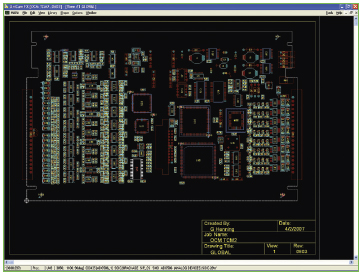
Figure 1. Working from the CAD system offers the best chance at accurate data.
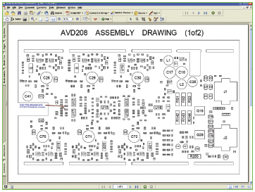
Figure 2. The assembly drawing provides higher-quality information about board assembly than do Gerber data and should
be included.
