

How new powders, activator chemistries and epoxy fluxes are evolving for production use.
History shows that the electronics assembly industry is always up for a good challenge. This was proved with the successful move from through-hole to SMT assembly, the elimination of CFCs from the cleaning process and implementation of Pb-free, to name just a few. Now, the industry is arguably at one of its biggest – er, smallest – challenges to date: extreme miniaturization. Although device footprint reduction has been an ongoing process over the past two decades, recent developments are some of the most exigent to date. Although designing much smaller packages presents its own unique set of hurdles (a topic for another article), the ability to incorporate these microscopic components into a high-volume, high-reliability production environment is at issue for assembly specialists.
Placing 0201s and 0.4 mm CSPs in a lab environment is one thing; achieving this feat reliably in high-volume manufacturing is quite another. A plethora of process variables are impacted by this reality, none likely as complex as the soldering process. Not only must solder materials accommodate much tighter pitches and smaller geometries, they also must maintain all the previously established requirements for modern manufacturing, including Pb-free capability, compatibility with higher reflow temperatures, humidity resistance, wide process windows and much more.
These new conditions pressure tried-and-true rules for solder materials such as stencil aspect ratios and surface-area-to-volume requirements. Here, we describe several developments on the solder materials front – from new powders to activator chemistries to epoxy flux technologies – to meet miniaturization trends.
As use of ultra fine-pitch devices grows and industry moves from 0201s to 01005s and from 0.4 mm CSPs to 0.3 mm CSPs, prevailing Type 3 solder pastes will no longer be sufficient to address smaller deposit volume requirements. Simply moving from Type 3 to Type 4, however, will not necessarily deliver the desired result either. Type 4 materials must be optimized for miniaturization demands.
In this instance, optimizing means tightly controlling not only the particle size, but the distribution of those particles within the material. While current industry standards tend to be a bit unclear as to allowable particle size in the upper end of the range, J-STD-006A (Table 1) is fairly liberal with the distribution range of particle sizes. But, recent testing has suggested a tighter distribution range and a smaller upper limit particle size may prevent some problems down the line.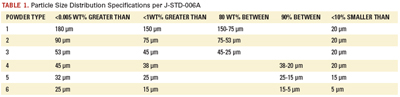
Current work has focused on not only condensing the distribution and size range of the Type 4 particles, but also on producing the powder in such a way that the integrity of the surface finish is maintained, as this is also essential to lowering oxidation risk. The smaller particles of Type 4 materials make for a higher surface-area-to-volume ratio, which, in turn, introduces more opportunity for oxidation. Left uncontrolled, oxidation can lead to a variety of performance issues, including non-coalescence, poor wetting, or graping (more on that later), to name just a few. New powder production technology has delivered consistent, smooth surfaces, even on powder spheres less than 35 µm in diameter.
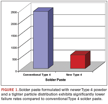
What’s more, by tightening the particle size distribution, the paste release from the stencil is much more complete. Larger particles can easily become trapped in the miniaturized apertures, leading to insufficients and down-the-line defects. By significantly reducing the upper and lower limits on the particle size in newer generation Type 4 materials, high-speed printing through 80 µm-thick stencils with 150 µm apertures becomes a much more robust process (Figure 1).
Pb-Free Solder Advances
Powder technology not only is critical in the move to much finer dimensions, but the overall capability of the paste and, specifically, the flux system is key. As 0201 integration has increased in production environments – particularly in the handheld sector – demands on smaller paste deposits have caused new process issues to emerge.
One such problem is graping. This phenomenon, which is partially coalesced solder that resembles a cluster of grapes, is directly attributable to extreme miniaturization (Figure 2). The cause of graping is easily understood, but not easily remedied without proper solder materials. With much smaller solder paste volumes, the solder particle surface-area-to-flux ratio is pushed to a point at which flux exhaustion occurs, the relative level of surface oxidation increases, and graping is the result. 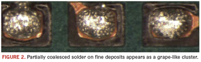
Flux’s function within the solder paste is to permit the formation of a solder joint by eliminating oxides that are present on metal surfaces – including the spheres within the paste. In addition, flux should protect the paste particles during reflow so as to prevent re-oxidation. As miniaturization requirements dictate the use of much smaller particle sizes (i.e., Type 4 and, in some cases, Type 5), the total metal surface of the solder increases and, therefore, demands more activity. Most powder oxidation occurs on the particles that are on the surface of the deposit. This puts more demands on the flux as the relative amount of solder surface is increased. Surface oxides generally melt at a higher temperature, and with older-generation formulations, the flux cannot overcome this condition.
By incorporating novel materials development technology, however, there are several ways to alleviate graping. As mentioned, smooth surface powders with a much tighter distribution range and upper/lower particle size limit greatly improve paste release from the stencil, deliver more even deposits, and provide a reduced metal surface and ideal deposit surface-area-to-volume ratio.
Next-generation solder paste flux formulations have proved that by providing sufficient activity and re-oxidation mitigation capabilities, graping can be resolved literally as it is occurring. Figure 3 illustrates this result, as traditional solder materials are compared to newer materials that have been optimized for miniaturization processes.
It also is important to note that while altering the flux and powder to accommodate for new process conditions, materials must also maintain their reliability requirements, as well as surface insulation resistance (SIR) and electrochemical migration (ECM) performance.
Heterogeneous Component Placement
Another obstacle presented by extremely miniaturized components is the dilemma about how to place the large and small components most efficiently. While new solder pastes are capable on both large- and small-volume deposits, stencil technologies are often the limiting factor. Designing a stencil capable of printing the large and small deposits in a single sweep is nearly impossible. A second print is out of the question, so the solution becomes dip fluxing.
Traditional dip fluxes certainly deliver the activity required to promote robust solder joint formation; the problem is how to then protect those joints. Capillary flow underfills will work only if there is a gap large enough to permit sufficient flow and coverage. Because this is a relatively large “if” considering newer component geometries, an alternative methodology should be considered.
The process is identical, but the material – an epoxy flux – is vastly different. Epoxy flux materials combine the solder joint formation action of a flux and the protection of an underfill into a single material. On a printed circuit board where one might need to place 0.3 mm CSPs, other very small types of area array devices or even flip-chip-on-board, epoxy flux is ideal for many reasons.
First, because the material combines the dual-functionality of a flux and an underfill, the secondary underfill dispense process can be eliminated. With epoxy flux, the solder joint is formed, and the epoxy surrounds and protects each interconnect during reflow. Second, even when capillary underfilling is an option, traditional underfill materials have exhibited problems such as component floating and voiding. A fluxing underfill, however, stays around or near the solder bumps to add an extra level of reliability without inducing floating or void formation.
For manufacturers faced with the heterogeneous – large and small – component conundrum, epoxy flux is an excellent option.
The Nano Future
An article on solder materials science would be sorely lacking without a discussion of what the future may hold. Temperature concerns and development of novel thermal management techniques are, with the advent of very small devices and Pb-free processes, more top of mind than ever. And, while significant progress has been made in relation to temperature control, applying knowledge from other markets may provide clues to soldering’s future.
As a case in point, transient liquid phase sintering (TLPS) is being evaluated as a thermal management solution. Used successfully in ceramic applications, the possibilities for TLPS in electronics manufacture are intriguing. TLPS processes rely on the combination of low-temperature melting alloy powders combined with higher-melting metal powders, which, when processed above the melting point of the lower temperature alloy, fuse to form a new intermetallic compound that will not re-melt at that same temperature but rather a much higher temperature. For electronics, this could conceivably mean that devices could be manufactured at significantly reduced temperatures and be able to withstand higher Pb-free processing temperatures with no risk of re-melt or damage. TLPS for electronics is very much in the infancy stage, of course, but many companies in the soldering industry are investigating its potential.
As technology marches on, so does materials innovation. In fact, in many cases, materials innovators are far ahead of the parade – developing materials for next-generation applications a good three to five years from becoming mainstream. These latest solder materials developments are further evidence of the ingenuity and expertise at the foundation of our industry. Solder solutions such as advanced powder technologies, more capable flux formulations, and dual-function materials such as epoxy fluxes are all enabling the smaller, faster, cheaper demands of the consumer to be fulfilled.
Solder materials science has indeed gotten small, but only because of big ideas and large innovation initiatives from leading materials scientists.
Neil Poole, Ph.D., is a senior applications chemist at Henkel Technologies (henkel.com); neil.poole@us.henkel.com. Brian Toleno, Ph.D., is senior applications chemist – assembly materials at Henkel.
A master trainer assesses the revised industry guidelines for PCB acceptability.
The visual acceptance criteria for post-assembly soldering and mechanical assembly requirements, IPC-A-610, Acceptability of Electronic Assemblies, was recently “up-reved” as it tries to keep pace with the numerous new component packaging types and other changes to electronics assemblies. The “D” revision, published in 2000, ushered in Pb-free acceptance criteria at the time RoHS standards were put in place. The new “E” revision addresses some more recent technologies since the last revision was published.
The standards task groups made several changes to the Revision “E” document, including but not limited to package-on-package (POP) and leadless device packages, flexible circuits, board-in-board connections and newer style SMT terminations.
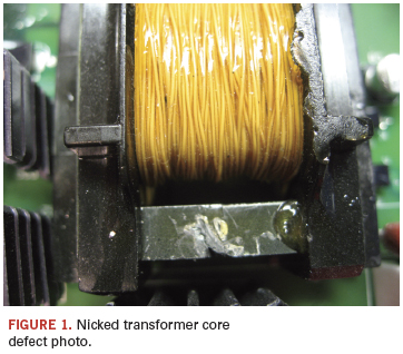
One area where there was a noticeable change is damaged components (found in Section 9 in the new document). Where the previous version held all the information associated with a damaged component termination style under the section on those part types, now all damaged components are in the same section. This will save users time flipping between the various sections. Specifically, sections on damaged transformer, connector and relays are the most significant upgrades.
There have been upgrades to Section 8, the area array section of the standard. This section now deals with differences in both wetting and collapse characteristics of Pb-free solder balls. Since very few area array devices are available with tin solder balls, this is a welcome upgrade. While this is a welcome change, users still complain about the lack of detail in this section.
Another device type that has exploded in terms of its usage since the printing of the last version is the leadless device package. These are addressed in the new revision, also in Section 8. While the revision offers expanded inspection criteria, it does not go far enough in defining the criteria for the myriad different package types available today.
One of the other changes made to this version is the organization of terminals as found in Section 6. For each terminal type, an easy-to-use table guides the user through the plethora of different combinations of different terminal types and their acceptance criteria.
Lead cutting into solder is fully explained with clear photos for through-hole devices in this new revision – a welcome change, as this is an area of confusion among users that should be put to rest. The new photos leave no ambiguity as to where a lead can or cannot be cut vis-a-vis the solder fillet.
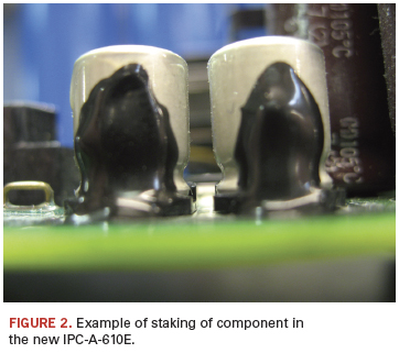
In Section 8, photographs and further explanations help clarify how staking adhesives can be used when mechanically securing components to the board. Section 8 also deals with leadless device terminations, flattened post terminations, as well as other specialized SMT connections.
Flex circuitry criteria for damage, flex stiffeners, soldering flex to flex and flex to PCBs are a welcome upgrade.
Some training organizations have commented that the new standard more closely parallels existing IPC training materials. As my colleague Norman Mier observes, “The new IPC-A-610 format allows for enhanced references that I am sure will improve the training and, more importantly, the comprehension and usage of this important tool for the factory floor.” Training materials for IPC-A-610E are slated to be released in late summer or early fall. In the meantime, students can be certified to the “D” revision and can recertify to “E” in the future.
A free fact sheet and a redlined version highlighting the changes to the document are available from the IPC website.
Bob Wettermann is president of BEST Inc. (solder.net); bwet@solder.net.

Can high-mix, low-volume production succeed in China? You bet.
In the 1970s, if you set up a contract manufacturing shop in a good location, customers eventually would walk through the doors. In the real world, things quickly changed for American companies, as OEMs, driven by maximizing shareholder value, searched for cheaper sources offshore. The first options were Hong Kong, Malaysia and Singapore. After prices increased in these countries, greener pastures were found in China. Unfortunately, as the saying goes, all good things must end.
Believe it or not, “Made in China” does not mean cheap anymore. Outsourcing to China was a trend that became popular starting in the mid 1990s. At that time, demand for China sources far outweighed the supply, driving up prices. Along the way, China accrued sizable foreign exchange reserves filled with US greenbacks, with the trade deficit between the US and China hitting $226 billion by 2009.
With mounting pressure from the US government and the World Trade Organization, China has begun to loosen trade restrictions. It has decided to shift toward manufacturing higher value goods, so the trade deficit “quotas” are not wasted on lower-margin products like Tupperware and toys. China has taken a three-step approach to doing this: First, it has selectively increased import duties on materials used in the manufacturing of low-value products. Second, it has dramatically improved the employment conditions of factory workers by demanding significant increases in paid benefits and minimum wages. Third, it is slowly phasing out free trade zones and licenses.
The free trade license, known as san li yi bao, permits companies, many from Hong Kong, to set up production facilities in China without paying any import duties or value-added taxes. The caveat is that all products manufactured must be exported. This was introduced by Prime Minister Deng Xiao Ping in the late ’80s as a means of attracting investments so that the post-Mao Chinese could work in meaningful jobs, as opposed to laboring away on farms. This program certainly succeeded in meeting its goals. China, with a population of 1.3 billion people, is now facing a massive labor shortage. As of February, the China Times reported, the Pearl River Delta area faced a shortage of two million workers.
My company, Season Group, is a global EMS provider with a mega-site in Dongguan, among others. Like others in China, we are facing these issues. How do we cope? By being open to change. As Charles Darwin wrote, “It is not the strongest of the species that survives, nor the most intelligent, but the one most responsive to change.”
Growing up, I was often discouraged to enter contract manufacturing, as it operates in what some term a “herd-like mentality.” This means contract manufacturing always goes wherever labor is the cheapest, just as herds do when grazing. Unlike the pastures, though, cheap labor does not return to a country once a higher wage has been set. This means cheap labor becomes scarcer, and all businesses must be prepared for it.
When Western OEMs formulate their outsourcing strategy, they must maintain a strict protocol: Low-mix, high-volume (LMHV) work is outsourced to Asia, while all high-mix, low-volume (HMLV) work stays onshore. HMLV is by nature more complex, as the same amount of preparation work needs to be done at a higher frequency when comparing HMLV to LMHV. The characteristics of HMLV work make strong communication between OEM and EMS partners a must, which gets difficult when different languages, cultures and time zones come into play.
Here’s where Darwin comes in. Foxconn, the world’s largest EMS provider, has announced a fully automated production facility in Taiwan as a test run. If successful, it will emulate this plant throughout China so that it is not bound by labor shortages. Season will continue to invest internationally as a means of diversifying our risks. Our Penang, Malaysia, facility will be expanded to replicate our China site, with vertically integrated manufacturing capability, including wire harness assembly, PCB assembly, mold and die making, plastic injection molding and plastic thermoforming. This facility provides us with stabilized costs, as wages in Malaysia have not changed much in the past 10 years.
Not all products are suitable for offshore production: low-volume, bulky, IP-sensitive, national security, etc. In the near future, there will be a surge of de-sourcing activities in Asia that will result with the production sent back to the US.
If you think your current manufacturing strategy is optimal and can last an eternity, be ready for a rude awakening. With economic dynamics changing on a daily basis, no strategy is permanent. Many in the textile industries rushed to Bangladesh in 2009 due to favorable economic circumstances compared to Vietnam; thus, land prices – and subsequently, labor prices – were driven up. Now, with the Vietnamese currency down to 18,885 dong per $1 (from highs of 16,000 per $1), it makes sense to look at Vietnam again. When outsourced assembly work started leaving the US shores for China in the mid 1990s, few thought it would ever come back. The current trend of onshoring proves no strategy is ever safe.
Carl Hung is vice president - Season Group (seasongroup.com); carl.hung@seasongroup.com.

Properly applied DfM mitigates component package tolerances.
You may have been here: John and Sally did the design and PCB layout for their company’s popular new product. It was, in fact, so popular, many of the primary-source components cannot be procured in the quantity necessary, so backup sources have begun to be used.
And that’s when the trouble began. Instead of the high yield they had been achieving, there were failures and, worse, intermittent problems began to surface. After a great deal of time investigating the cause, they discovered one of the components supplied by a secondary supplier was not quite mechanically equivalent. Unlike the initially sourced part, the solder points did not line up in the center of the lands.
This can happen with any product. However, very popular products that run for a long time are more likely to have to use second- or third-source parts over the run of the product. And, of course, a long-running, popular product is the last one in which you want to have quality problems arise.When a designer uses a land pattern for a single-sourced component, such as a programmable part, SoC, etc., the chance for subsequent manufacturing problems, due to the component not precisely matching the lands, is virtually zero. Lands were specifically designed for that, and only that, part. On the other hand, commodity-type parts are almost always multi-sourced, and not all suppliers have precisely the same component geometry.
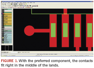
Here’s a real-world example: Figure 1 shows the contacts area of one possible component placement. Notice the size of the left and right distance present to supply enough solder on each side of the pin. In this example, the preferred component’s contacts fit neatly into the center of the lands generated from library data. Even if the component were slightly misplaced or dislodged, there is a cushion. Such margins enhance manufacturability and minimize rejects.
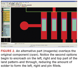
In Figure 2, a second-source component placement has been superimposed over the primary-source component. The cyan color represents the original component, and the magenta color represents the portions of the second-source component that extend beyond the bounds of the primary-source component. This part is now encroaching on the edges of the lands. Because the contact points take up greater area on the land, less solder is available to form an acceptable pin filet. While the component in this illustration may not produce manufacturability problems, in more extreme cases, contact points might take up too much area, or be near or off the edge, which can result in serious quality problems.
Rather than find out you have a problem when production yields take precipitous plunges, incorporate DfM practices early in the design process to ensure all possible components will be accommodated by the land patterns in the design library. (This, by the way, can be automated.)
On the horizon are tools capable of automatically generating an “envelope” that fits all available components. Then, the envelope is compared to the land patterns. Using the envelope approach ensures every possible component that can be sourced for this product will fit and pass a solderability test.
This problem is just one that can be addressed with DfM techniques and tools. In the future, I will illustrate other DfM techniques for PCB design.
Max Clark is product marketing manager, Valor Division, Mentor Graphics (mentor.com); max_clark@mentor.com.
Why visual indicators as a cleanliness gauge may be dangerous practice.
Preventing field failures due to electrochemical migration used to be relatively easy: Use a water-soluble flux and clean the board after soldering. This solution no longer holds true, and sometimes causes more problems than it prevents.
Water-clean fluxes, also known as organic acid (OA) fluxes, are often preferred over no-clean products for high-reliability applications because of their higher activity. They are more effective at removing oxides, promoting wetting and overcoming solderability variations. Problems arise when their residues are not fully cleaned from the assembly. OA fluxes are active at room temperature, and all they need to begin damaging the assembly is DC voltage and atmospheric moisture. When OA flux residues remain on a circuit assembly, the concern is not a matter of if the circuit board will fail; it is a matter of when it will fail.
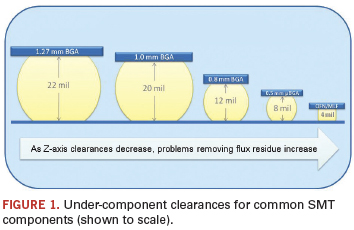
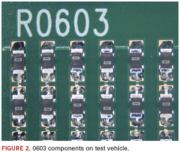
Fully cleaning the harmful residues gets increasingly difficult as components get smaller and standoff heights shrink (Figure 1). Many low-standoff components are designed only for no-clean soldering processes; however, OEMs and assemblers sometimes have no choice but to use them in water-clean applications. And without a definitive, nondestructive test for cleanliness, both parties harbor concerns about the long-term reliability of the end-product.
To characterize the cleanability of modern OA solder pastes, a simple experiment was devised. PWBs were assembled with 12 of the industry’s most popular pastes, reflowed in an air atmosphere, cleaned, and visually graded for residues.
Areas easily reached by the wash process, like gullwing or J-lead components, were represented by unpopulated component pads printed with solder paste. Areas obscured by low-standoff components like µBGAs or QFNs were conservatively represented by 0603 components (Figure 2). Reflow was performed in an ERSA Hotflow 3/20, 10-zone reflow oven using typical thermal profiles for SnPb and Pb-free (SAC 305) alloys, and cleaning was performed in a Speedline Aquastorm AS200 inline cleaner at a belt speed of 2 ft./min. Water temperatures of 120°, 140° and 150°F were used. Three boards were processed at each setting; the three scores were averaged and reported.
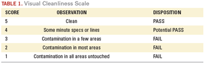
The gold standard for assessing cleanliness is ion chromatography (IC), but performing IC analysis on a large sample size is time-consuming and cumbersome. To rapidly assess flux residue cleanability, a visual cleanliness scale
(Table 1) was developed. It should be noted that visual cleanliness does not necessarily indicate ionic cleanliness, but visible residues generally do indicate residual ionic contamination. Therefore, the only grade on this scale that could be considered a “pass” is a 5. Several areas assigned a score of 5 were confirmed clean with ion chromatography. Scores of 4 or more indicate that the reflow and/or cleaning process could likely be dialed in to produce acceptable results. Scores of 3, 2 or 1 are unacceptable process failures.
Test Results
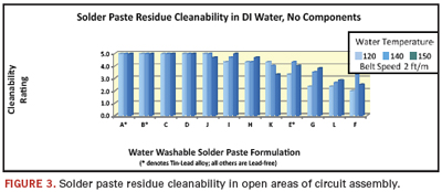
The first test assessed the overall process friendliness of the solder pastes by evaluating their cleanability on unobstructed pads using only deionized water. Results (Figure 3) are ranked in order of their cleanability. Of the 12 pastes tested:
- Five demonstrated easy cleanability.
- Two posted scores in the 4+ range, indicating potentially good cleanability.
- Five pastes failed.
- Two of the failures showed exceptionally poor cleanability.
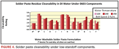
The next test mechanically removed the 0603s and examined the post-cleaning residue underneath. Figure 4 presents them in the same order as in Figure 3.
Under-component cleaning results differ substantially from the bare board results:
- Paste A, which demonstrated best-in-class cleanability in visible areas, actually showed the worst results in obstructed areas.
- All the pastes left some degree of residue.
- Three pastes scored 4s at some, but not all, temperatures.
The average cleanliness scores of visible and obstructed areas were then compared (Figure 5). The comparison produced eye-opening results:
- Only one of the five pastes that demonstrated excellent cleanability in the open areas showed good cleanability under the components. The other four received failing grades.
- The two pastes that showed potential for good cleanability on the bare board areas showed similarly good cleanability in the obstructed areas (pastes H and I).
- The three pastes that produced obviously unacceptable results in the visible areas produced similarly unacceptable results in non-visible areas.
- Half the pastes tested showed substantial drops (more than one grade point) in cleanability when the different areas are compared.
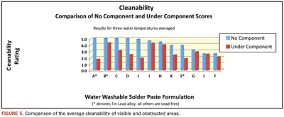
The cleaniness differences between the two areas are obvious – what you see is not necessarily what you get. Relying on visual indicators to gauge an assembly’s cleanliness may be dangerous practice, depending on the solder paste formulation and processes to which it has been exposed.
The ionograph test that is commonly used to monitor cleaning processes’ effectiveness can also lull users into a false sense of security. In many cases, the alcohol-water mixture in the test solution does not completely dissolve baked-on residues under the low-standoff components, and the test fails to detect the actual contamination levels. Even if it does fully dissolve the residues and detect all the contamination, the test averages it across the entire surface area of the assembly, diluting the localized dangerous level to a perceived overall “safe” level.
Improving Cleanliness
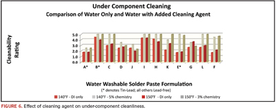
The next phase of the experiment added a cleaning solution to the wash. Cleaning agents work in two main ways: They lower the surface tension of the water so it can reach into tight areas, and they help act on the residues to dissolve them.
At wash temperatures of 140°F, introduction of a cleaning agent at a 5% concentration dramatically improved under-component cleaning. At 150°F, only a 3% concentration was required to produce similar results (Figure 6). Introduction of cleaning chemistry, even at low concentrations, made a substantial impact on the cleanliness of the areas obscured by the low clearance components:
- In 12 of 24 cases, the introduction of a cleaning agent produced a perfect score of 5. When cleaning agents were not used, no perfect scores were recorded over the course of 72 trials.
- In all cases except one, the addition of chemistry improved cleanliness under the component.
- Pastes L and F, which demonstrated some of the poorest cleanability with DI water alone, scored 5 and 4+ when cleaning agents were added to their wash process.
For many years, OA solder pastes were referred to as “water-soluble.” Recently, that term has migrated to “water-washable” or “water-cleanable,” indicating that modern formulations do not exhibit the easy solubility of their predecessors. The current data support this migration of terminology, demonstrating that residues under components can be satisfactorily washed away – but not with water alone.
Consider trying to wash a car, household laundry or dirty dishes with water only. The car, clothes or dishes would be extremely difficult to clean without the assistance of detergents. Industrial cleaning processes are no different from domestic ones; they all work better when they incorporate cleaning agents. In the case of circuit assemblies and modern solder pastes, cleaning chemistries are rapidly becoming a necessity. For low-standoff components like microBGAs and QFNs, engineered cleaning solutions are assuring ionic cleanliness and alleviating the concerns of electrochemically induced field failures for everyone in the supply chain.
Harald Wack, Ph.D., Umut Tosun, Joachim Becht, Ph.D., and Helmut Schweigart, Ph.D. are with Zestron (zestron.com); hwack@zestron.com. Chrys Shea is founder of Shea Engineering Services (sheaengineering.com).
Chip caps are prone to leakage, so consider these test methods for minimizing electrical failures.
Capacitors are widely used for bypassing, coupling, filtering and tunneling electronic circuits. However, to be useful, their capacitance value, voltage rating, temperature coefficient and leakage resistance must be characterized. Although capacitor manufacturers perform these tests, many electronics assemblers also perform some of these tests as quality checks. This article looks at some of the challenges associated with capacitor testing, as well as some of the test techniques used.
A capacitor is somewhat like a battery in that they both store electrical energy. Inside a battery, chemical reactions produce electrons on one terminal and store electrons on the other. However, a capacitor is much simpler than a battery because it can’t produce new electrons – it only stores them. Inside the capacitor, the terminals connect to two metal plates separated by a non-conducting substance known as a dielectric.
A capacitor’s storage potential, or capacitance, is measured in farads. A one-farad (1 F) capacitor can store one coulomb (1 C) of charge at one volt (1 V). A coulomb is 6.25´1018 electronics. One amp represents a rate of electron flow of 1C of electrons per second, so a 1 F capacitor can hold one amp-second (1 A/s) of electrons at 1 V.
The coulomb’s function of an electrometer can be used with a step voltage source to measure capacitance levels ranging from <10pF to hundreds of nanofarads.
The unknown capacitance is connected in series with the electrometer input and the step voltage source.
The calculation of the capacitance is based on this equation:
Figure 1 illustrates a basic configuration for measuring capacitance with an electrometer with an internal voltage source. The instrument is used in the charge (or coulombs) mode, and its voltage source provides the step voltage. Just before the voltage source is turned on, the meter’s zero check function should be disabled and the charge reading suppressed by using the REL function to zero the display. (The purpose of zero check is to protect the input FET from overload and to zero the instrument. When zero check is enabled, the input of the electrometer is a resistance from roughly 10 MΩ to 100 MΩ, depending on the electrometer used. Zero check should be enabled when changing conditions on the input circuit, such as changing functions and connections. The REL function subtracts a reference value from actual readings. When REL is enabled, the instrument uses the present reading as a relative value. Subsequent readings will be the difference between the actual input value and the relative value.)
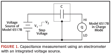
Then, the voltage source should be turned on and the charge reading noted immediately. The capacitance can then be calculated from:
where
Q2 = final charge
Q1 = initial charge (assumed to be zero)
V2 = step voltage
V1 = initial voltage (assumed to be zero)
After the reading has been recorded, reset the voltage source to 0 V to dissipate the charge from the device. Before handling the device, verify the capacitance has been discharged to a safe level. The unknown capacitance should be in a shielded test fixture. The shield is connected to the LO input terminal of the electrometer. The HI input terminal should be connected to the highest impedance terminal of the unknown capacitance. If the rate of charge is too great, the resulting measurement will be in error because the input stage becomes temporarily saturated. To limit the rate of charge transfer at the input of the electrometer, add a resistor in series between the voltage source and the capacitance. This is especially true for capacitance values >1 nF. A typical series resistor would be 10 kΩ to 1 MΩ.
Capacitor Leakage
Leakage is one of the less-than-ideal properties of a capacitor, expressed in terms of its insulation resistance (IR). For a given dielectric material, the effective parallel resistance is inversely proportional to the capacitance. This is because the resistance is proportional to the thickness of the dielectric, and inverse to the capacitive area. The capacitance is proportional to the area and inverse to the separation. Therefore, a common unit for quantifying capacitor leakage is the product of its capacitance and its leakage resistance, usually expressed in megohms-microfarads (MΩ·µF). Capacitor leakage is measured by applying a fixed voltage to the capacitor under test and measuring the resulting current. The leakage current will decay exponentially with time, so it’s usually necessary to apply the voltage for a known period (the soak time) before measuring the current.
In theory, a capacitor’s dielectric could be made of any non-conductive substance. However, for practical applications, specific materials are used that best suit the capacitor’s function. The insulation resistance of polymer dielectrics, such as polystyrene, polycarbonate or Teflon, can range from 104 MΩ·µF to 108 MΩ·µF, depending on the specific materials used and their purity. For example, a 1000 pF Teflon cap with an insulation resistance higher than 1017 Ω is specified as >108 MΩ·µF. The insulation resistance of ceramics such as X7R or NPO can be anywhere from 103 MΩ·µF to 106 MΩ·µF. Electrolytic capacitors such as tantalum or aluminum have much lower leakage resistances, typically ranging from 1MΩ·μF to 100 MΩ·µF. For example, a 4.7 µF aluminum cap specified as 50 MΩ·µF is guaranteed to have at least 10.6 MΩ insulation resistance.
Capacitor leakage test method. Figure 2 illustrates a general circuit for testing capacitor leakage. Here, the voltage is placed across the capacitor (CX) for the soak period; then the ammeter measures the current after this period has elapsed. The resistor (R), which is in series with the capacitor, serves two important functions. First, it limits the current, in case the capacitor becomes shorted. Second, the decreasing reactance of the capacitor with increasing frequency will increase the gain of the feedback ammeter. The resistor limits this increase in gain to a finite value. A reasonable value is one that results in an RC product from 0.5 to 2 sec. The switch (S), while not strictly necessary, is included in the circuit to allow control over the voltage to be applied to the capacitor.
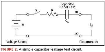
The series resistor also adds Johnson noise – the thermal noise created by any resistor – to the measurement. At room temperature, this is roughly 6.5×10¹⁰ amps, p-p. The current noise in a 1 TΩ feedback resistor at a typical 3 Hz bandwidth would be ~8×10-16 A. When measuring an insulation resistance of 1016Ω at 10 V, the noise current will be 80% of the measured current.
Alternate test circuit. Greater measurement accuracy can be achieved by including a forward-biased diode (D) in the circuit (Figure 3). The diode acts like a variable resistance, low when the charging current to the capacitor is high, then increases in value as the current decreases with time. This allows the series resistor used to be much smaller because it is only needed to prevent overload of the voltage source and damage to the diode if the capacitor is short-circuited. The diode used should be a small signal diode, such as a 1N914 or a 1N3595, but it must be housed in a light-tight enclosure to eliminate photoelectric and electrostatic interference. For dual-polarity tests, two diodes should be used back to back in parallel.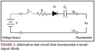
Test Hardware Considerations
A variety of considerations go into the selection of the instrumentation used when measuring capacitor leakage:
- Although it is certainly possible to set up a system with a separate voltage source, an integrated one simplifies the configuration and programming process significantly, so look for an electrometer or picoammeter with a built-in variable voltage source. A continuously variable voltage source calculates voltage coefficients easily. For making high-resistance measurements on capacitors with high voltage ratings, consider a 1000 V source with built-in current limiting. For a given capacitor, a larger applied voltage within the voltage rating of the capacitor will produce a larger leakage current. Measuring a larger current with the same intrinsic noise floor produces a greater signal-to-noise ratio and, therefore, a more accurate reading.
- Temperature and humidity can have a significant effect on high-resistance measurements, so monitoring, regulating and recording these conditions can be critical to ensuring measurement accuracy. Some electrometers monitor temperature and humidity simultaneously. This provides a record of conditions, and permits easier determination of temperature coefficients. Automatic time-stamping of readings provides a further record for time-resolved measurements.
- Incorporating switching hardware into the test setup allows automating the testing process. For small batch testing in a lab with a benchtop test setup, consider an electrometer that offers the convenience of a plug-in switching card. For testing larger batches of capacitors, look for an instrument that can integrate easily with a switching system capable of higher channel counts.
Configuration examples. Producing enough useful data for statistical analysis requires testing a large quantity of capacitors quickly. Obviously, performing these tests manually is impractical, so an automated test system is required. Figure 4 illustrates such a system, which employs an electrometer with built-in voltage source, as well as a switching mainframe that houses a low current scanner card and a Form C switching card. In this test setup, a single instrument provides both the voltage sourcing and low current measurement functions. A computer controls the instruments to perform the tests automatically.
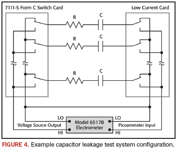
One set of switches is used to apply the test voltage to each capacitor in turn; a second set of switches connects each capacitor to the electrometer’s picoammeter input after a suitable soak period. After the capacitors have been tested, the voltage source should be set to zero, and then some time allowed so the capacitors can discharge before they are removed from the test fixture.
Note that in Figure 4 the capacitors have a discharge path through the normally closed contacts of the relays. To prevent electric shock, test connections must be configured in such a way that the user cannot come in contact with the conductors, connections or DUT. Safe installation requires proper shielding, barriers and grounding to prevent contact with conductors.
More complex test systems that combine leakage measurement with capacitance measurements, dielectric absorption and other tests, if desired, are possible. A simplified schematic of such a test system using an LCZ bridge and a picoammeter with a voltage source is shown in Figure 5.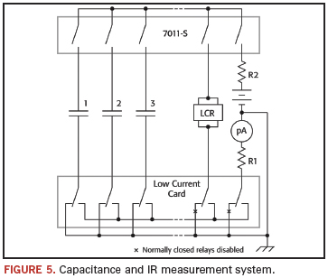
Test System Safety
Many electrical test systems or instruments are capable of measuring or sourcing hazardous voltage and power levels. It is also possible, under single fault conditions (e.g., a programming error or an instrument failure), to output hazardous levels, even when the system indicates no hazard is present. These high-voltage and power levels make it essential to protect operators from any of these hazards at all times. It is the responsibility of the test system designers, integrators and installers to make sure operator and maintenance personnel protection is in place and effective. Protection methods include:
- Design test fixtures to prevent operator contact with any hazardous circuit.
- Make sure the device under test is fully enclosed to protect the operator from any flying debris.
- Double insulate all electrical connections that an operator could touch. Double insulation ensures the operator is still protected, even if one insulation layer fails.
- Use high-reliability, fail-safe interlock switches to disconnect power sources when a test fixture cover is opened.
- Where possible, use automated handlers so operators do not require access to the inside of the test fixture.
- Provide proper training to all users of the system so they understand all potential hazards and know how to protect themselves from injury.
Dale Cigoy is lead applications engineer at Keithley Instruments (keithley.com); dcigoy@keithley.com.

Press Releases
- Altus Adds LPKF CuttingMaster 3290 to Depaneling Portfolio
- Kurtz Ersa Partners with E-tronix for Sales in Illinois and Wisconsin
- XLR8 EMS Welcomes Raul Jorge Lopez Jr. as Director of Program Management and Procurement
- Koh Young America Promotes Ramiro Mora to Lead Service and Applications in Mexico and South America