

Reaffirming the Relevance of the Area Ratio Rule

How using a thinner stencil corrected transfer efficiency.
SMT specialists are intimately familiar with the guiding rule of stencil printing: the area ratio. The correlation between stencil aperture dimensions and the predictability of solder paste transfer efficiency is well understood, and IPC has standardized design guidelines outlining ideal conditions. The accepted area ratio for maximum transfer efficiency is approximately 0.60, which is a function of the aperture open area and aperture wall area (stencil thickness). When the area ratio falls below the recommendation, challenges arise.
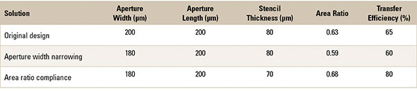
Reaffirmation of the relevance of the area ratio rule occurred recently when our company was asked to analyze a customer assembly where bridging was observed. The printing dimensions of the PCB’s bridging area were tight. The 01005 apertures measured 200µm x 200µm, the stencil thickness 80µm and the interspace about 150µm. So, while not at the bleeding edge like some newer-generation designs, the board was nevertheless challenging. With these aperture dimensions, the area ratio was an acceptable 0.63. The volume of paste on pad was 2.08 nanoliters (NL), and the standard deviation was less than 10%, but SPI analysis revealed bridging.
For its part, the customer had logically attempted to lessen the bridging propensity by narrowing the aperture width to reduce the amount of solder paste being transferred onto the pad. Unfortunately, doing so resulted in conflict with the area ratio rule, and taking this route ultimately impacted repeatable transfer efficiency.
IPC has illustrated this with its aperture guideline (FIGURE 1). In any situation where the ratio is 1 or greater, the transfer efficiency expectation is 80% or more. In other words, one would anticipate the theoretical volume of material deposited onto the pad at 80% minimum. When the area ratio is tightened, the transfer efficiency begins to drop off, and the standard deviations from the aperture increase dramatically. No longer is it guaranteed the same volume of material will be released from the aperture print after print, and this is what the customer experienced.
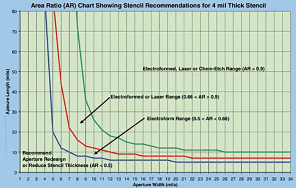
Figure 1. IPC area ratio curve.
In this application, when the aperture perimeter was reduced to 200µm x 180µm, the area ratio dropped below the acceptable 0.6 slightly to 0.58; the standard deviation increased to greater than 10%; and the transfer efficiency landed at 60%, with paste-on-pad volume at an average of 1.7NL. For high-volume manufacturing, this is not acceptable. The goal in this case was to reduce volume from 2.08NL, but within a 4 Sigma process and a less than 10% deviation with ideal 80% transfer efficiency. To comply with the area ratio rule and this aperture dimension, the only solution was to use a thinner stencil.
“But how?” you may ask. Historically, stencils came in standard thicknesses: 150µm, 125µm, 100µm, 75µm, and so on. If that were still the case, the math wouldn’t work from an area ratio perspective for this application. Times have changed, however, and today’s stencil manufacturers can produce just about any thickness desired with no preset limits. For our customer’s situation, reducing the thickness of the stencil to 70µm would permit the print to stay within the area ratios.
One also might assume if the material volume is reduced, interconnect issues may result. However, in looking at IPC’s area ratio curve, thinning the stencil with the reduced aperture size increases the area ratio, delivering more efficiency out of the aperture. And that’s exactly what happened. When the stencil thickness was set at 70µm, and aperture dimensions were maintained at 180µm x 200µm, the standard deviation was again less than 10%, as in the original design, but transfer efficiency increased dramatically to 80%, and material volume was 2.0NL (TABLE 1). Once again, the area ratio rule prevailed, and the bridging issues were resolved. Stencil printing is not a sport for rule-breakers.
Table 1. Transfer Efficiency of Different Approaches
(Caveat: This was a miniaturized assembly for a mobile device. For a heterogeneous PCB that requires large material volumes in some areas, the use of a step stencil would allow compliance with the area ratio rule to allow for increased paste volumes for specific components.)
is global applied process engineering manager at ASM Assembly Systems, Printing Solutions Division (asmpt.com); clive.ashmore@asmpt.com. His column appears bimonthly.


