Pretty Slick

Paste particle size can influence solder printability, but not as much as nanocoating.
We’ve been doing a lot of print testing in our lab. In our first set of published results, “The Impact of Reduced Solder Alloy Powder Size on Solder Paste Print Performance” from IPC Apex 2016, we revealed a hierarchy of input variables to maximize solder paste transfer efficiency and minimize variation. In that study, we used a fully-optioned stencil as part of the equipment set. To tease out the data we were looking for, we could not lose critical information to the noise of stencil-induced variations.
If the stencil in that study were an automobile, it would be a Bentley. It was made by a consistently top-performing manufacturer, using the best materials, workmanship and flux repellent coatings as determined by prior studies. Its combination of precision automation and meticulous craftsmanship helped create very clean data for our analysis, which gave us great direction for understanding the finer points of the process and characterizing our products under ideal conditions.
In the real word, we can’t all drive Bentleys, but some options we can’t live without. (Remember when keyless entry was a luxury item?) When our vice president of technology, Karl Seelig, reviewed our print data, he was extremely impressed, but immediately asked what it would look like if the stencil weren’t nanocoated.
Hence, this latest installment in our deep dive on printing technologies.
We asked our stencil supplier to make us the same stencils, using the same materials, machines and operators, but without the nanocoating. Let’s call this one the Cadillac of stencils; by eliminating the nanocoating, the price of the stencil can be cut by as much as half. But coating is not the only added expense that cost-conscious buyers balk at. So is Type 5 solder paste, so we repeated our tests using both T5 and uncoated stencils, looking for trade-offs.
The new leg of testing was performed on the same test vehicle in our in-house applications lab by the same engineers and on the same equipment. It used the same formulation of solder paste as the previously published DoE, but used only fresh T4 and T5 pastes, and it directly compared the powder size and nanocoating print performance.
How do we judge a good print? Our benchmark for a robust print process is a minimum of 80% solder paste transfer efficiency (TE) with a standard deviation of 10% or less than of the mean. Standard deviation as a percentage of mean is also known as the coefficient of variation, or CV. Therefore, we analyze our data looking for TE ≥ 80% and CV ≤ 10%. We focused on print features with area ratios (ARs) of 0.50 to 0.75, so when using a 4 mil (100µm) foil, we looked at feature sizes from 8 to 12 mils (200 – 300µm). The area ratios and theoretical aperture volumes (in cubic mils) are shown in TABLE 1.
Table 1. Details for Each Pad Size Analyzed
In both the original and supplemental studies, pad definition was found to have significant impact on print quality; solder-mask-defined pads (SMD) demonstrated lower deposit variation with less overall volume, whereas non-solder-mask-defined pads (NSMD) produced greater deposit variation but with greater volume. In fine-feature printing found on 0201 or 01005 chips, LGAs, BTCs or other leadless packages, limiting paste deposit variation is a greater priority than applying higher paste volume. Stencil aperture designs can be modified to increase deposit volume, whereas inconsistent deposits are an uncontrolled liability. FIGURE 1 illustrates the effect of SMD and NSMD pads.

Figure 1. Effect of pad definition on solder paste print quality.
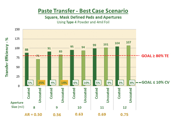
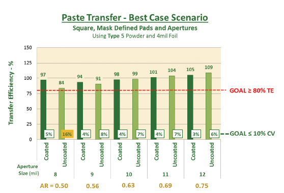
Let’s apply the pass/fail criteria of TE ≥ 80% and CV ≤ 10% to the data shown in FIGURES 2 and 3.

Figure 2. Transfer efficiency and CV of Type 4 powder at various area ratios (ARs).

Figure 3. Transfer efficiency and CV of Type 5 powder at various area ratios (ARs).
We begin by analyzing the variation (CV) with the objective of 10% or less. When using T4 paste, that goal can be achieved on an AR of 0.50 using a coated stencil. However, we cannot reach our goal with an uncoated stencil until the AR is 0.63. T5 solder paste was successful at AR of 0.50 with a coated stencil, but not until an AR of 0.56 with an uncoated stencil.
So what’s better for the process? Hands down, the nanocoated stencil, since it only changes one variable in the process. Using a T5 solder paste can introduce additional process variables, including print, reflow and working life properties and can be a burden on the supply chain with increased cost and limited availability.
Now let’s consider transfer efficiency. With an uncoated stencil, Type 4 paste did not achieve either the 80% TE cutoff or the 10% CV cutoff on ARs of 0.50. It barely eclipsed the TE benchmark on the 0.56 AR but with unacceptably high CV. The Type 5 met the ≥ 80% TE criteria with all ARs on both stencils, but failed to meet the CV benchmark at 0.50 without the help of the nanocoating.
Again, what’s better for the overall process? Nanocoating. When overlaying the results, T4 pastes printed using nanocoated stencils met the criteria for print quality at all ARs tested, and performed nearly identically with T5 pastes at ARs of 0.63 and up. Furthermore, even when an uncoated stencil met the benchmark, it still demonstrated about twice the variation of its coated counterpart. If a microns-thick coating can cut print variation in half, it can help both miniaturized and mainstream assemblers keep yields up and repair costs down.
Another observation on the nanocoating influence on TE: It is providing a boost in the low AR ranges, but not in the higher ones. This means we can consistently expect more paste on our fine feature prints, while keeping our larger prints stable.
The data we just reviewed were the best-case scenario: SMD square pads and apertures. We also investigated the worst-case scenario – NSMD circular pads and apertures – and everything in between. We studied print peaking and print definition differences by comparing heights and areas respectively. We also measured the differences in print quality between standard and high tension foil mountings. Stay tuned, because all these data will be published at SMTA International in Rosemont, IL, on Sept. 27 and in upcoming issues of CIRCUITS ASSEMBLY.
As fine-pitch devices are migrating from the consumer/handset world into every facet of PCB assembly, performance gains are literally measured in microns, and are typically incremental and compounding. This mass migration is again driving suppliers to find the most proven materials and reliable techniques for their mainstream users. Will we add more stencils or conditions to our print database? Undoubtedly. The exact nature of the data will depend on our customers’ needs and, of course, our veep’s next question.
is technical marketing manager at AIM Solder (aimsolder.com); toneill@aimsolder.com.
Press Releases
- Koh Young Webinar to Show How Data Transparency Strengthens SMT Production Resilience
- Aven Welcomes Max Ramos to Strengthen Distribution Partner Operations
- ubersmt Expands SMT Line with Juki G-Titan Printer and RS-1R Placement System
- Keiron Technologies to Host LiFT Webinar Focusing on Solving Solder Paste Printing Challenges


