Void Reduction on QFNs

Sometimes the answers to the most tenacious questions are right under your nose.
As I sit in Chicago’s O’Hare Airport having just left another productive and exciting SMTA International trade show, I reflect on what an excellent opportunity this event presents to network and stay current in the world of electronics assembly. If you don’t attend these events regularly, you should. I was fortunate to have the opportunity to attend a number of the technical conference sessions and not only learn what is emerging, but also speak with customers and colleagues on what they see as the most pressing needs of the market. "
To sum it up … BTC void reduction. The technical sessions on void reduction I attended were all standing room only, and the topic was the subject of many hallway conversations among technologists. The presentations offered supplier and user perspectives on materials and techniques that have been tested both in the lab and the field with varying degrees of success in reducing voids. A few themes were repeated: Solder paste formulation is the biggest single variable that aided in void reduction; profiling techniques can definitely help mitigate voids, and pad/via/stencil design is extremely important. The bottom line remains the same, however: It will always be difficult to evacuate 50% of the volume of the printed deposit in the form of gaseous flux during a typical reflow cycle with limited outgassing paths.
Those who have been following our recent series of articles know that we have been actively performing print studies to ensure we have the processes and materials to meet the requirements of the ever-shrinking solder features on PCB assemblies. During these tests, my esteemed colleagues in our Juarez, Mexico, applications lab noticed something unusual while studying the I/O pads on QFN. If they didn’t print the I/O pads, they saw a dramatic reduction in voids on the ground pads. And by dramatic, we mean dramatic. There were no measurable voids on a component that otherwise exhibited voids in the 10 to 15% range. This piqued their interest, as all the ground pads on the test board were printed with the typical “window pane” pattern at about 70% coverage.
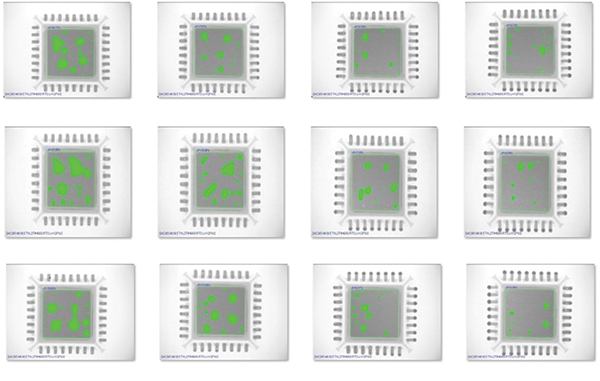
Following their instincts, the engineers decided to pursue manipulating the print volume on the I/O pads to determine whether there was a design that would promote void reduction. Up until now, much of the industry testing has focused on manipulating the ground pad paste deposit, not the I/O deposit. Window panes, star bursts, hourglass, diamonds, herringbones, and every other aperture shape imaginable have been tried on ground pads, all with the same objectives of providing outgassing pathways for flux volatiles and manipulating the volume of solder. Our experience has been that these ground pad aperture designs have some impact on void mitigation, but not the ultimate answer. These preliminary results, however, were the first time we have seen the volume of solder paste on the I/O pads impact void formation on the ground pad. FIGURE 1 shows the degree of impact the I/O aperture design had on ground pad voiding in the initial tests.

Figure 1. Void reduction on BTC ground pads as a result of changing I/O aperture design while maintaining the same ground pad aperture design on the original experiment.
These results were unexpected and profoundly positive. However, the sample size was small and was only on one package size. The skeptics in AIM’s technical department needed more data to be convinced there was something to it. What ensued was a full-fledged design of experiments (DoE) that employed a variety of QFN sizes and I/O pad designs to attempt to repeat the outcomes.
FIGURE 2 shows the results of I/O aperture manipulation on QFN grounding for a variety of process conditions. These results clearly indicated a correlation between I/O pad design and a significant reduction in ground pad voids. We are currently engaged in an even deeper study by manipulating more variables and introducing the I/O design to a production environment to determine how repeatable and robust this technique can be. Every strategy that can be deployed to reduce voiding – especially those that do not require significant capital investment – represents an important opportunity to improve product quality.

Figure 2. Repeated results in reduced voiding resulting from I/O aperture design in larger DoE with more input variables.
This development not only has exciting potential, it also highlights the importance of attending industry events. We are looking forward to providing CIRCUITS ASSEMBLY readers with the big-picture overview and sharing all the critical details of this testing within our SMT community at upcoming events. Reflecting on this most recent SMTAI conference, I realize much of the information that both users and suppliers seek is right under our noses. These industry events, whether local, regional or international, enable us to witness the latest advancements and see the opportunities to improve quality, productivity and efficiency, all under one roof. I can’t wait for the next one. See you there!
is technical marketing manager at AIM Solder (aimsolder.com); toneill@aimsolder.com.
Press Releases
- Kitron Secures EUR 37M order for Next-Generation Tactical Communication Equipment
- Scanfil Comparison Figures for Updated Customer Groups
- Javad EMS Invests in Inovaxe Smart Storage Carts to Streamline Material Management and Boost Production Efficiency
- ViTrox Announces Strategic Partnership with High Tech Solutions (HTS) to Strengthen Presence in Argentina


