High frequency current wants to concentrate near conductor edges. How to compensate for it.
Skin effect is the tendency of high-frequency current to concentrate near the outer edge, or surface, of a conductor, instead of flowing uniformly over the entire cross-sectional area of the conductor. The higher the frequency, the greater the tendency for this effect to occur.
There are three possible reasons we might care about skin effect:
- The resistance of a conductor is inversely proportional to the cross-sectional area of the conductor. If the cross-sectional area decreases, the resistance goes up. The skin effect causes the effective cross-sectional area to decrease. Therefore, the skin effect causes the effective resistance of the conductor to increase.
- The skin effect is a function of frequency. Therefore, the skin effect causes the resistance of a conductor to become a function of frequency (instead of being constant for all frequencies.) This, in turn, impacts the impedance of the conductor. If we are concerned about controlled impedance traces and transmission line considerations, the skin effect causes trace termination techniques to become much more complicated.
- If the skin effect causes the effective cross-sectional area of a trace to decrease and its resistance to increase, then the trace will heat faster and to a higher temperature at higher frequencies for the same level of current.
Faraday’s Law (of magnetic induction) is the fundamental principle behind EMI and crosstalk. It is also the fundamental principle behind a motor or a generator. Simply stated, Faraday’s Law says A changing current in one wire causes a changing magnetic field that induces a current in the opposite direction in an adjacent wire.
But here is the step that is not particularly intuitive. If a changing current in wire A can cause a changing magnetic field, and that changing magnetic field can induce a current in the opposite direction in an adjacent wire B, then that changing magnetic field can also induce a current in the opposite direction in wire A, itself. This is the fundamental nature of inductance.
Consider a wire, A. Assume the current in wire A suddenly increases. At the very first instant of time, there is a changing magnetic field around A that induces a current in the reverse direction in A that cancels out the original current. The net change in current in A is zero. At the very next instant of time, the changing magnetic field around A begins to decay slightly, and a small amount of net current begins to flow. At the very next instant of time, the changing magnetic field decays a little more, and a little more net current begins to flow. This process continues during successive instances of time until the full increment of current is flowing along the wire. This is the nature of inductance and describes the effect of inductance on current flow.
Suppose the process described above is interrupted. Let’s say halfway through, the original current suddenly changes direction. Now the process starts over, but this time in the opposite direction. Every time the original current changes direction, the process starts over in the reverse direction. The number of times the original current changes direction each second is the frequency of the current. If the frequency is high enough, the full current never gets to flow across the entire cross-section of the wire.
Now, during this process, here is the question: During the period of time in which the magnetic field is decaying, where does the current flow? It flows where the magnetic field is weakest. And the magnetic field weakens the further it is away from its source. Its source is along the center of the conductor. So the current that does flow tends to flow strongest the further the distance from the center of the conductor – that is, along the outer surface. This is the skin effect.
Steady-state currents flow uniformly across the entire cross-sectional area of the conductor. When we think about the skin effect, we tend to think in terms of the current flowing only at the outer surface. This is not really true. The issue really is current density. Normal currents have a current density that is uniform and equal everywhere over the cross-sectional area. But currents impacted by the skin effect have a current density that is highest at the surface of the conductor, decaying exponentially between the surface and the center of the conductor.
If current density is represented by J, then:
where
Jo = current density at the surface of the conductor
e = base of the natural logarithm (2.718).
d = distance measured from the surface toward the center of the conductor
sd = skin depth
Figure 1 illustrates the two cases of uniform current density, and current density impacted by the skin effect.

Skin depth. Skin depth is defined as the point where the current density is the current density at the surface (Jo) divided by e, or![]()
The skin depth defines a cylindrical shell at the circumference of a wire or a rectangular shell around a trace. We tend to think in terms that the current flows uniformly through that shell, and not anywhere else along the conductor. Therefore, the effective cross-sectional area of the conductor is that shell, and the effective resistance the current sees is the resistance defined by that shell. But if current density follows an exponential function from the surface to the center of the conductor, then this can’t be the case. The true effective cross-sectional area only can be determined by using calculus; i.e. integrating the area under the current density curve.
Here is the interesting thing. It can be shown mathematically that multiplying the current density at the surface (Jo) by the cross-sectional area defined by the skin depth will result (at least approximately) in the same answer as if calculus techniques were used. Therefore, using the effective cross-sectional area defined by the skin depth works, even though it does not represent the actual truth.
We say the skin depth defines the effective cross-sectional area of the conductor not because this is true, but because it works!
Skin depth is inversely proportional to the square root of the frequency (in hertz):
Two very important things should be noted here: First, skin depth does not depend on the shape of the conductor. Skin depth is a distance measured in from the surface of the conductor toward the center of the conductor. Second, if skin depth is deeper than the center of the conductor, the current is not limited by the skin effect, and the current is flowing uniformly throughout the entire cross-sectional area of the conductor. Therefore, a thicker conductor is limited by the skin effect at a lower frequency than is a thinner conductor.
Crossover frequency. Consider a rectangular trace. For simplicity we will consider it to be much wider than it is thick. At low frequencies, the skin depth is deep enough that it extends further than half the trace thickness, and therefore, the skin effect does not come into play. At higher frequencies, the skin depth is smaller than half the thickness, so the effective cross-sectional area is limited by the skin effect. There is a unique frequency where the skin depth is just equal to half the thickness of the trace. This is the frequency where the skin effect just starts to come into play. This frequency is called the crossover frequency.
Calculating the crossover frequency can be difficult. For a rectangular trace, I estimate it as:
re
f = crossover frequency
w = trace width
t = trace thickness
A graph of crossover frequency as a function of trace thickness is shown in Figure 2. Skin effect calculations can be difficult. Calculators are available that simplify the calculations by determining several skin effect parameters, including the crossover frequency of a trace, and then frequency adjusted resistance values at user defined frequencies.

Proximity and ground effects. If frequency is high enough so that the effective cross-sectional area of a conductor is limited by the skin effect, there are two other effects that may also need to be considered. When a signal is close to its return, a mutual inductance exists that may further distort the current flow. Consider a rectangular trace routed directly over and close to a reference plane. If the frequency harmonics are high enough, the skin effect results in the current flowing through an effective cross-sectional area that is a rectangular shell around the edges of the conductor. At the same time, the mutual inductance between the signal current (on the trace) and its return (on the plane) causes the return current to locate itself as close as possible to the signal – i.e., on the plane directly under the trace. This same effect causes the signal current in the rectangular shell to locate more on the planar side of the shell than on the outer side of the shell. This effect is called the “ground effect” (Figure 3).

A similar effect occurs when a signal and its return are on closely spaced wires or traces – as is the case with differential signals. The mutual inductance between the two traces causes the signal currents to distort to the side of the effective cross-sectional area between the two traces. This is termed the “proximity effect.”
Since the proximity and ground effects distort the current path of the signals through the conductors, they further distort the effective cross-sectional area of the conductor, further increasing the effective resistance of the conductor. These effects are very difficult to quantify. Howard Johnson suggests they might be on the order of 30% or so, and he has a good discussion of this on his website.2
Lossy transmission lines. The skin effect, by changing the effective cross-sectional area of a conductor, causes the effective resistance of the conductor to change with frequency. This is of little consequence for most designers most of the time. But there is one circumstance where it becomes very important to PCB designers. The skin effect is one of the two primary causes of losses in lossy transmission lines (the other is dielectric losses.)3
When signals flow down a wire or trace, they reflect back again. The issue is whether we care about this reflection. And we do care if the line is “long” relative to the rise time of the signal.4 The solution to the reflection problem is to design our trace to look like a transmission line and then terminate the line in its characteristic impedance. Figure 4 shows a model of an ideal transmission line and the formula for the characteristic impedance. Of importance is the fact that the characteristic impedance has no phase shift at any frequency, and therefore, it is purely resistive at every frequency.

Figure 5, however, shows what happens to a transmission line model at high frequencies when the skin effect (and dielectric losses) come into play. Of particular significance is the fact that there is no single-valued resistor that can properly terminate such a line at every frequency.

The classic symptom of a lossy transmission line is an eye diagram that starts closing. Properly terminating lossy transmission lines is much more complicated than terminating “lossless” lines.5 When frequencies become high enough that the skin effect becomes a factor in traces, the resulting transmission line losses become one of the more significant signal integrity challenges for board and system design engineers.
References
1. Ultracad.com/ucadpcb.htm.
2. Howard Johnson, “Signal Effect Calculations,” sigcon.com/Pubs/news/skineffect.htm.
3. For a good discussion of these two effects, see Howard Johnson and Martin Graham, High-Speed Signal Propagation, Prentice Hall, 2003, pp. 185-216.
4. Douglas Brooks, Signal Integrity Issues and Printed Circuit Board Design, Prentice Hall, 2003, chapter 10, pp. 175-203.
5. Ibid., chapter 17, pp. 311-320.
Douglas Brooks, Ph.D., is president of UltraCAD Design Inc. (ultracad.com); dgbarticles@dgbpersonal.com.
Understanding the new standard for predicting temperature rise.
Determining appropriate trace sizes for current requirements is an important aspect of board development. Since copper is not a perfect conductor, it presents a certain amount of impedance to current flowing through it, and some of the energy is lost in the form of heat. For many applications, it is necessary to predict the temperature rise caused by this loss, which traditionally has been accomplished using a chart created over 50 years ago by the National Bureau of Standards (IPC-2221, Figure 6-4), or by using one of several calculators based on it. The chart shows the relationship between current, conductor temperature rise and conductor cross-sectional area. If any two of these are known, the third can be approximated.
About 10 years ago, Mike Jouppi, then of Lockheed Martin, began performing experiments to examine the accuracy of this chart, because the predicted temperature obtained from it did not correspond to the data he was measuring on actual product. From these new data, he developed several new charts, which have been verified by a parallel study performed by the Naval Surface Warfare Center, Crane Division.
The results of both studies were compiled into IPC-2152, “Standard for Determining Current Carrying Capacity in Printed Board Design.”1 From the data in this new document, a method can be established to predict the temperature rise of a board trace more accurately, taking into account the effect of several variables such as board thickness and material, internal vs. external traces, still air environments vs. vacuum, and proximity to heat-sinking planes.
Estimations using these new data can be far more reliable than previously possible, without the use of more sophisticated thermal analysis tools.
IPC-2152 contains over 90 new charts in addition to the now infamous historical chart, but before exploring the new data, a few aspects of the historical chart should be understood. When the chart was created in the 1950s, there were no multilayer boards, and all the data were taken from surface traces. No one is sure where the internal chart came from, but it is thought that when multilayer board constructions became practical, the external values were merely doubled to get values for internal traces. This has since proven inaccurate. The thermal conductivity of FR-4 is better than air, so in a still-air environment, internal traces run cooler than external ones. The internal values are so conservative, however, that designers haven’t experienced problems using them, except for the large amount of board real estate needed to implement the recommendations.
An interesting result of the new study is that, although the values for internal traces were not scientific, by coincidence they very closely approximate the behavior of traces in free air. The new data also show the external trace chart only was safe for boards greater than 3 x 3˝ and with planes, so it was decided to remove the historical chart for external traces from IPC-2152. Recommendations for external traces can be easily obtained with the new charts and adjusted for the proximity to heat-sinking planes.
Because the internal chart values approximate the temperature rise of a trace in free air (which can be considered a worst-case scenario), it was decided to use it for the most conservative chart (Figure 1). Values obtained from this chart are very safe and will work in any circumstance except vacuum, regardless of other variables.
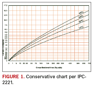
For example, let’s say a trace in a very thin flexible dielectric must carry 4 A continuously, and you want to limit the temperature rise to 10°C over ambient. To use the conservative chart, follow the 4.0 A current line across until it intercepts the 10°C temperature curve. Follow that intersection down to find the recommended cross sectional area of 0.300˝2. This cross-sectional area can be refined further by modifying it with known design constraints. These adjustments are described in Modifying the Chart Value.
After the recommended cross-sectional area is determined, it can then be converted to appropriate trace widths (based on the copper thickness used in the design) by using a chart presented later in this article.
Figure 1 provides very safe estimates for most applications. For a more precise estimate based on specific design constraints, new charts have been developed. Since board development often depends on common laminate materials with common copper weights, separate sets of charts are provided based on 0.070˝ polyimide material with 3, 2, 1 and 0.5 oz copper in still air. For each of these, there is a primary logarithmic chart (Figure 2). Figure 2 is the baseline chart for 3 oz. copper, which is the universal chart used in IPC-2152, Figure 5-2, and recommended for both internal and external traces.
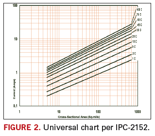
Since logarithmic charts are difficult to read, three additional charts that show temperature curves at successively finer resolution follow each of these primary charts. This has been duplicated by another complete set of charts for vacuum environments, and all these are duplicated again to provide versions for inch and metric units. (There are also charts in the appendix for internal vs. external traces.)
(For the purposes of this tutorial, we will look up a starting value from the universal chart and then modify it for our particular design constraints. If you have the extra charts in IPC-2152, you can select a chart more specific to your application, and skip the corresponding modification outlined below.)
Obtaining the Appropriate Chart Value
The first step in estimating appropriate trace widths is determining the acceptable temperature rise. This is an important point, because most board designers are familiar with “ambient temperature,” a simple term that describes the environment in which the electronics assembly operates. For our application, “ambient temperature” can be misleading, because the temperature rise of the trace is going to be higher than all the contributing factors combined. This is not just the ambient temperature; it is the ambient temperature plus all the other heat sources of nearby components and traces.
For this reason, the new standard prefers the term “local board temperature” to “ambient temperature.” The local board temperature can be significantly higher than the surrounding environment, and the temperature rise of a single trace is added on top of that. For example, the product may be required to operate in an ambient temperature of 125°C, and the area of the trace evaluated may have power devices and other high current traces in close proximity. The local temperature already may be approaching the maximum continuous operating temperature of the board material itself, and a lower temperature rise may need to be defined for the single trace. (Parallel traces are a critical factor that should not be ignored. The added temperature from surrounding traces can have a significant effect on the local board temperature, and should be considered in every evaluation. IPC-2152, Appendix A.3.3, discusses this in detail.)
In general, traces operating at high temperature waste power and add thermal stress that may lead to early failure, so a low temperature rise should be a design goal whenever possible.
Once you have settled on an acceptable temperature rise for the trace being evaluated, it is a simple matter to find the cross-sectional area required for the current requirement, using either the conservative chart or the new universal one. (Use the new one only if your board is greater than 3x3˝!)
Modifying the Chart Value
If the conservative chart (Figure 1) was used to obtain the starting chart value (CV), it can be used as is, without additional analysis. If the universal chart (Figure 2) was used to obtain the CV, keep in mind that it is based on a board that was constructed with 3 oz. copper on polyimide 0.070˝ thick. To get a more accurate estimate, several modifications may be performed to the CV. The easiest way is to start with a modifier of 1.00, then add or subtract based on the following paragraphs to get the final modifier, then multiply the modifier and the CV to get the modified cross-sectional requirement.
Start with a modifier of 1.00, and go through the following steps:
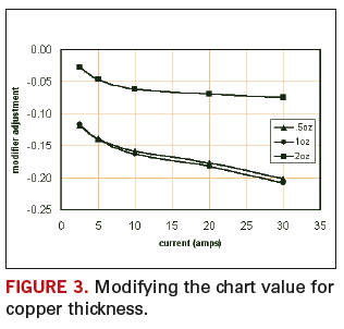
1. Copper thickness modifier. If the universal chart was used to obtain the CV, and something other than 3 oz. copper is used, take advantage of the fact that for the same cross-sectional area, thinner copper has more surface area and is therefore better at dissipating heat. Thicker copper will have thinner trace width for the same cross-sectional area, less surface area, and will operate at a higher temperature (Figure 3).
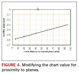
2. Plane modifier. Because the proximity to heat-sinking planes has such a drastic impact on the temperature, the presence of planes will cause the most significant adjustment to the CV. For boards with a 1 oz. plane that is at least a 3 x 3˝ area (directly under the trace being evaluated!), use Figure 4 to determine the modifier:
For 2 oz. planes, subtract another 0.04 from the modifier.
For planes greater than 5 x 5˝, subtract another 0.04 from the modifier.
3. Board material modifier. The polyimide material used in the study has a thermal conductivity of 0.0138˝, and FR-4 is slightly worse at 0.0124˝, which makes a difference of about 2% in the CV. Materials with different thermal properties may influence the recommendation. For FR-4 boards, add 0.02 to the modifier (Figure 5).
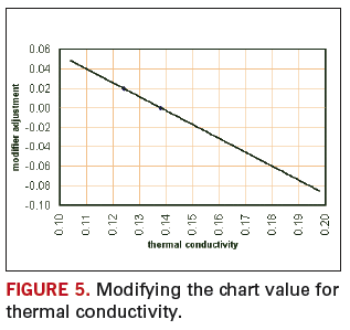
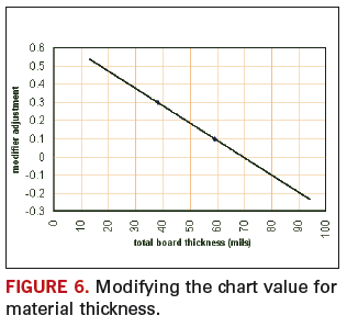
4. Board thickness modifier. The new charts were constructed using data from 0.070˝-thick boards. Thinner boards will be hotter, and thicker boards will be cooler (IPC-2152 A.4.2) (Figure 6).
5. Altitude modifier. This one may be refined in the future, but knowing that air is thinner at higher altitude, and traces run 35 to 55% hotter in a vacuum, either the conservative chart should be used or the CV should be increased for high-altitude designs.
6. Derating modifier. Keep in mind the charts have no derating applied, but many variables may affect the CV prediction and should be considered for marginal designs. For example, the planes modifier is based on the assumption that the trace sits over a solid plane, but in actual practice may be located near a board edge or over a plane that has clearances in it for through-holes or plane splits, which will be less effective in dissipating heat. Process variations that affect the trace geometry may also influence the results (in the form of voids, nicks, overetching, final plated conductor thickness, etc.). These variations all have acceptable tolerances in the finished product, but may affect the estimated temperature rise. It is advised that some amount of standard derating be applied to the CV – 5%? 6%? – but a full examination of this modifier is beyond the scope of this article.
7. Environmental modifier. The new data describe traces in still air (which assumes some amount of natural convection), so these recommendations should be valid even for applications inside a sealed enclosure. But for many other applications, airflow will be present, and this additional heat transfer may allow a reduction in cross-sectional area. This is a complicated subject, and recommendations related to airflow are beyond the scope of this article.
Some thermal analysis may be needed if the designer needs to use thinner traces than what the available data suggest.
Obtaining the Final Trace Width
At this point you have selected a value from one of the charts and modified it for your specific design parameters. Multiply the starting CV with the final modifier to get the final recommended cross-sectional area for the application.
The final step is converting the resulting cross-sectional area to the final trace width, based on the thickness of copper used in the board construction. This step should not be confused with the modification based on copper thickness to account for varying surface area. Figure 7 is a direct correlation between cross-sectional area and (copper thickness x trace width):
For example, assume the design of a four-layer FR-4 board that will be 3 x 5˝ by 0.063˝ thick, and the two internal layers are power and ground planes that are 0.020˝ away from the surface layers. We need a trace that can accommodate 4 A continuously, and we want to limit the temperature rise to 10°C above the local board temperature.
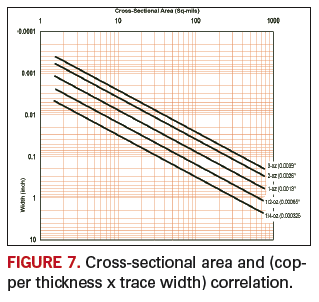
We could use the conservative chart to get a 0.300˝2 cross-sectional area, and use the final conversion chart for 1 oz. copper to get:
Trace width = 0.220˝.
That’s the easy answer, and if the board design allows, it can be used as is. Because we have good information about our design, and the board is larger than 3 x 3˝, the universal chart can be used instead. Following the 4 A line across to the 10°C temperature curve, we see that it intersects with the line for a starting value of 0.200˝ cross-sectional area.
CV = 200, starting modifier = 1.00
Next, we can modify based on 1 oz. copper:
Modifier = 1.00 – 0.14 = 0.86
Because we have a 1 oz. plane 0.020˝ away, using the Planes Chart, we get:
Modifier = 0.86 – 0.53 = 0.33
Our board thickness of 0.062˝ is less than 0.070˝, thus using the Thickness Chart:
Modifier = .033 + 0.10 = 0.43
We are using FR-4 instead of polyimide, so using Material Chart:
Modifier = 0.43 + 0.02 = 0.45
And as a judgment call, we add 3% for derating:
Modifier = 0.45 + 0.03 = 0.48.
Now we modify our starting 0.200˝2 chart value:
200 x 0.48 = 96
Using the final chart to convert 0.096˝2 to a 1 oz. trace width, we get:
0.007˝ trace width.
The historical chart would have recommended a 0.095˝ trace width for a 4 A, 1 oz. external trace, which illustrates how the new data can be used to push the envelope. In many cases, the design can have less board space, using appropriate parameters to derive the estimate.
References
1. IPC-2152, “Standard for Determining Current Carrying Capability in Printed Board Design,” August 2009.
Acknowledgments
Thanks to Borko Bozickovic for help in analyzing data and developing charts, and to Mike Jouppi for making it all happen.
Jack Olson, CID+, is a circuit board designer at Caterpillar Inc. (caterpillar.com); pcbjack@gmail.com.
Designers’ fight for proper recognition has lasted 20 years.
The question was a familiar one. “Pete, what can we do to raise the visibility of designers and acknowledge the role they play in product development?”
A marketing guru at one of the major PCB EDA companies asked me this. It sounded familiar because it is the same question I asked 20 years ago when I first went to work for Printed Circuit Design magazine. Fresh off a design job, I had been hired as the green editor with a new cause and a head full of ideas about what the magazine could do to focus on PCB design and designers.
Not long after, I met some folks who were trying to start a global organization for designers. Within a short time, the IPC got involved, and thanks to Gary Ferrari and Dieter Bergman, among others, the IPC Designers Council was born. The excitement was palpable. Soon, local chapters were springing up all over the world. Printed Circuit Design ran ads in the magazine and did mailings to our subscriber list to encourage participation. When time allowed, I attended meetings all across North America. Even my home chapter in Atlanta had around 50 members, and 30 to 40 designers and engineers regularly attended monthly meetings.
Looking for the glue that would hold the organization together, and a feather designers could put in their caps, the organization developed the Certified Interconnect Designer program. The CID program was intended to certify a designer’s core competencies in design based on IPC standards.
Many designers signed up and took the basic certification test, and the Council directors moved to add more modules to the program based on advanced technologies and techniques. Gary and Dieter were very involved in the effort, and poured their time and energy into the Council with gusto. For a time, all was right with the world. The council grew, and before long, there were close to 50 local chapters in North America and Europe holding regular meetings.
Then slowly, but perhaps inevitably, the air went out of the balloon. Attendance fell and chapters began to go inactive. Today the IPC lists 23 local chapters. I recently sent emails to the email addresses of all 23 chapter heads, asking whether the chapter was still functioning and what activities they had planned. I received answers from nine, although I know that at least two or three more remain active. Five said they had regular meetings, and the other four described their chapters as active, but in their words, “on life support.” (Funny how all four used the same words.)
What happened to the excitement? What about all the hard work the local folks put into building the organization and the dreams of an active, global organization for PCB designers? Apathy, workload and lack of leadership are the comments I hear most. Many local chapter officers served several consecutive terms and grew tired of handling the load. Some said that they had trouble finding speakers for the meetings, or felt there was no compelling message or reason for attending.
On the positive side, several chapters are very active. North Carolina holds a conference and trade show every year and has been very successful. The Austin (Texas) chapter holds a Vendor Night every August. But, even if all 23 chapters were active, it would not be a ground swell.
Getting back to the original question, I’m not sure what we can do. Let’s estimate an average 50 members for each chapter. With 23 chapters, that’s 1,150 members. No one has hard numbers on the size of the PCB designer community. At one time we estimated there were 100,000 designers and engineers involved in PCB design in North America alone. Even if the number were half that today (it’s probably more), then Designer Council membership would be 2% of the audience. Maybe that is a good number, but it does not sound that good to me.
Editor-in-chief Mike Buetow has come up with a couple ideas that we plan to use in the coming months to highlight significant contributions designers have made to a project. We’re also looking for ideas from you. Whether you are involved in design or fab, we want to hear what you think PCD&F can do to increase the visibility of designers and acknowledge the role they play in product development. Email me at pwaddell@upmediagroup.com or go to our blog at pcdandf.blogspot.com and make yourself heard.
Pete Waddell is publisher and design technical editor of Printed Circuit Design & Fab/Circuits Assembly; pwaddell@upmediagroup.com.
What happens when one size doesn’t fit all?
For most, the road forward centers on offering the lowest cost product, or providing exceptional and/or unique service, or being at the cutting edge of technological innovation. Most would probably agree the migration toward Asia originated with, and has prospered from, the pursuit of the low-cost business model. Exceptional service is ever evolving and often specific to end-market or geographically driven needs. Companies the globe over tailor their unique interpretation of service to the needs of targeted customers and markets. Many believe technological innovation, the backbone of our “high-tech” industry, to be the last bastion of strength for (higher-cost) Western companies. Offering cutting-, if not bleeding-, edge technology for demanding, R&D-focused OEM engineers working on the next-generation “wow” is continually mentioned as the hallmark of the remaining Western companies.
The problem is, maybe that paradigm is shifting.
Much has been said and written about the evolving electronics industry, its migration, and the cost drivers that have left as carnage once big-name and proud industry pioneers. What has emerged from those ashes are smaller, more technically “niche” focused companies that are lean and mean (read: minimally staffed) and evolving process and technical advancements (read: do it on the fly). These smaller companies think about intellectual property more as something linked to software they use rather than their expertise in providing product. Equally, technological advances are often, but not always, gauged via the rearview mirror of what it took to get an order out, rather than what might lie ahead if that new technology is applied to new applications.
What goes unacknowledged is where technology is being developed and with whose IP. Technology development is made public in several ways. Sometimes it takes the form of white papers presented at technology associations. Sometimes dramatic press releases reveal the latest, greatest product and refer to the IP developed to make it happen. Another, more easily understood method is to track the number of patents issued – in particular US patents. In this sense, the number of US patents issued related to printed circuit boards rapidly is being controlled by non-American companies. In particular, measured by patent applications, Chinese companies seem to be more technologically innovative and IP-creating than all North American companies combined!
What does this mean? One observation is that maybe some of the smaller companies – companies historically not staffed with R&D departments, not known for generating IP, and less worldly about the process of protecting the same – are now the de facto drivers of technological innovation. The message for all companies – large OEMs to circuit board fabricators to small design bureaus – is that with the demise of some of the larger R&D-driven fabricators, the offloading of PWB R&D by major OEMs to suppliers, and the need for everyone to become more focused on technology vs. just offering “me-too” capacity, the paradigm is shifting as to who and how technology may be developed. Smaller companies need to better understand IP and large companies need to better understand the emerging new supply base.
Understanding IP is very different from developing new technology. Designers understand well the importance of their ability to create IP. Fabricators, on the other hand, don’t. Most fabricators work on getting the job done – developing processes and capability to satisfy the immediate order – and don’t fully understand that those efforts are their IP. Many of those efforts are cutting edge and very patentable. All efforts to develop technology must be looked at equally as IP – not just the pain and suffering expended satisfying an order.
For smaller companies without formalized R&D initiatives, how they satisfy customer requirements needs to be reconsidered. Documentation needs to be developed to capture what is done, why, and with what end-result in a way that explains the R&D that went into creating the IP that led to higher technology. Any run-and-gun environment hates slowing to commit pen to paper, but the rewards can be huge. Short-term, R&D credits are available. Longer-term, the technology library is created so technologically savvy customers can see your company has the ability to provide value-add R&D to assist their ascendency. And finally, out of some efforts may be patentable, groundbreaking technology that profoundly differentiates your company from the pack. This may be the greatest opportunity: creating long-term value by applying what you already do to a more formal R&D process that yields global recognition in the form of patents.
For larger companies, the shift is to embrace smaller companies that offer needed unique niche technology, and are in the best position to further develop that technology. This requires much more active involvement and commitment to working with a greater number of companies, many of smaller size. The benefits, besides attaining the desired technological development, are to broaden the supplier base with companies that are equally committed to an OEM’s technological needs and servicing that company as a valued customer. Larger companies may find there are more committed suppliers in their backyard than they thought, and those companies are best able to satisfy technological development.
For all companies, the need to understand technology and IP needs revisiting. How technology is approached – how we view IP – will determine who in the future is in a leadership position. Our industry is once again at a fork in the road. Following the route focused on rethinking IP may well be the best path forward.
Peter Bigelow is president and CEO of IMI (imipcb.com); pbigelow@imipcb.com. His column runs monthly.
The near-term holds more failures and consolidation as firms struggle to maintain revenues and lower costs.
Finding the sweet spot in EMS is a subject contemplated by many. The answer is naturally dependent on the company’s size and core competency. Top-tier EMS firms often look to high-volume products to create their sweet spot – namely mobile phones and motherboards – assemblies that give their factories high production utilization rates, although often at very low margins. Lower-tier EMS companies concentrate in certain industry sectors such as industrial, medical and military/aerospace, where they can achieve the highest profit margins or value-add engineering and design services.
For the past 12 months, these product areas haven’t been so sweet. Perhaps more alarming, there are few signs of these sectors achieving any substantial recovery in the near future, for a variety of exogenous reasons. The rippling effect of unemployment has negatively impacted consumer spending and dampened demand for products EMS companies make, such as medical and consumer electronics, and service industries such as travel, while the deficit in government tax revenue has capped or reduced capital spending. Two industries – automotive and semiconductor capital equipment – have been hit so hard that electronics assembly in these sectors will take years to recover.
So while pundits are eager to be optimistic and speak of turnarounds and growth, it’s hard to see the EMS industry being vigorous and booming any time soon. This doesn’t mean there won’t be successful companies (as the ones with the best practices clearly demonstrate), but it does mean there will be more failures and consolidation over the next several years, while many firms struggle to maintain revenues and lower costs. The industry sweet spots will only be sweet for a select few.
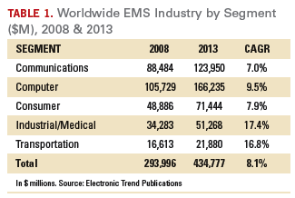
As we have been tracking this industry since 1993, we thought it useful to examine some trends and consider future possibilities. Per Table 1, it might be surmised that the EMS industry will remain fairly healthy for the next five years. Yet, the table does not illustrate the decline in revenue for 2009 (estimated at 6.6%), nor the gradual recovery over the ensuing years. It also doesn’t explain which product segments will grow fastest and have the most volume. (This information is contained within our annual syndicated report.) What this table does indicate, however, is approximately two-thirds of all EMS production can be found in the information technology industries (communications and computers), and the highest growth will be in the niche industries of industrial, medical and military/aerospace.
Another story emerges when we examine where industry growth will take place geographically (Table 2). While EMS revenue growth is below average in the leading geographic regions (except Asia), the strongest economic growth is expected to occur in the low-cost countries embedded within each region. Each year we examine over 40 individual countries for direct wage changes and economic growth, as well as account for the manufacturing footprint and capacity within. Based on our research, the nations expected to achieve the highest economic growth include Mexico, Eastern Europe, China and Vietnam, and “Other Rest of the World,” which includes India, Australia and South Africa.
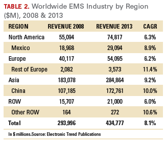
In the past, the leading driver in economic growth in these areas has been direct labor rates, an emerging factor is the need to exploit domestic markets. The trend to offshore for economic reasons has been abrogated by executives’ increased understanding of the total cost of manufacturing, which takes into account direct costs such as logistics, tariffs and transit time, as well as indirect costs, such as operations management, firefighting and the cost of money.
The low-hanging fruit has been gone a long time. Over the next several years, the successful EMS companies will be those that employ best practices (see our article in the October issue) and can achieve strong loyalty among their customers. Growth seems assured for EMS over the next five years. Success is not.
Randall Sherman is president and CEO of New Venture Research Corp. (newventureresearch.com); rsherman@newventureresearch.com. His column runs bimonthly.

Fall was the season of mergers and acquisitions: Viasystems and Merix; TTM and Meadville; DDi and Coretec. Likewise, you hold in your hands a merged product – PCD&F and Circuits Assembly. Like many of the industry deals, this was borne both of necessity and opportunity. The good news is, with our stable of editors, including Pete Waddell (20 years of design work), Kathy Nargi-Toth (a similar amount on the fabrication side), and my own 18-plus years covering design, fabrication and assembly, we have the technical chops and experience necessary to make sense of the fast-moving electronics manufacturing world. Going forward, our two brands will retain their identities, including their own websites. Meanwhile, the printed magazine – the last remaining monthly publication in North America covering electronics manufacturing – gets a boost in size and circulation. Win-win.
I have mixed feelings about DDi’s pickup of Coretec. On one hand, Coretec was finding it extremely difficult making it as a small yet publicly held company. Its sales had slipped from C$92 million in 2006 to C$81.4 million in 2008 – an 11.5% drop – and were on a run rate of $72.7 million this year. Worse, it was still seeing sequential declines through the September quarter, while competitor DDi has begun the upward revenue climb. Its last quarterly net profit was the fourth quarter 2006. And with no cash on hand, its hands were severely tied. All of which might explain why Coretec’s CFO position has been something of a revolving door for years.
DDI, on the other hand, has turned the corner after years of questionable acquisitions, two bankruptcies, and a notorious internal culture. It’s turned a profit all three quarters this year. That said, DDi has just $25 million in cash itself, and PWB fabrication is a cash-intensive business, with lots of ugly cycles. While I suspect DDi saw an opportunity to beat some competitors to the punch by bidding on Coretec now, I can’t help but think that had they waited, they might have picked up the company more cheaply. And I’d hate to see several years of work undone by a deal gone bad.
Meanwhile, TTM’s purchase of Hong Kong-based Meadville’s board business opens a huge can of worms, as it would put Hong Kong Chief Secretary for Administration Henry Tang in position to own 33% of TTM. But knowing a little about how government works, even when a Chinese government official is in line to become the largest shareholder of the leading bare board supplier to the US Department of Defense, it says here the real stunner would be if US anti-trust regulators saw a potential conflict and nixed the pending deal.
Warming in Munich. November’s biennial behemoth known as Productronica was, all in all, a better-than-expected show, modest by historical standards, but strong compared to everything else this year. Perhaps more important, after a year of malaise, there was a noticeable improvement in the general outlook for 2010. Almost across the board, the more than 80 companies we spoke with during the show see 2010 already emerging as a brighter year. The strong consensus is that the worst is past, and while there remain certain structural problems – including major banks’ inability or refusal to reopen credit lines – business is picking up in most sectors, led – perhaps surprisingly – by automotive.
Much like the two major China shows and Apex, Productronica this year was dominated – capital D – by regional visitors. And I am coming to believe the ongoing regionalization has less to do with the economy and more to do with the fact that for the very most part, existing production technology can build even the latest and greatest products. No matter that new generations of end-products come out every six months (or less), processes are driven by component packaging, and while leading-edge package types have shrunk from 0402 to 0201 to 01005 during the past five years, most conventional equipment is so darn good that it can print, place, solder, inspect and test the latest package styles. Assemblers simply no longer need to chase the latest and greatest equipment around the globe to win or build the latest designs. And that, in turn, obviates the need to run from show to show in search of the “next big thing.”
Year ends. KeyTronicEMS is one assembler that never has been the “next big thing,” but based on a six-year track record of net profits, it clearly should be in the conversation. Be sure to check our profile of the Circuits Assembly EMS Company of the Year this month.
2010 will bring our third annual Virtual PCB trade show and conference. This year promises to be the best yet. Click on www.virtual-pcb.com to learn more.
Our sincere hope that all our readers have a healthy, happy 2010!
Press Releases
- Kitron Secures EUR 37M order for Next-Generation Tactical Communication Equipment
- Scanfil Comparison Figures for Updated Customer Groups
- Javad EMS Invests in Inovaxe Smart Storage Carts to Streamline Material Management and Boost Production Efficiency
- ViTrox Announces Strategic Partnership with High Tech Solutions (HTS) to Strengthen Presence in Argentina


