Augur valve technology has enabled practical printer/dispensers.
It’s been on the wish list of low-volume, high-mix manufacturers for years: a printer that can also dispense adhesives. For assemblers that aren’t running high-volume operations and may only need to dispense in a few areas, purchasing an inline automated dispenser seems just a bit excessive – especially in today’s economy! So, having the ability to reduce floor space, save on capital equipment costs and obtain dispense capability all on a single printer is the panacea some assemblers have been looking for.
While designing such a system may sound simple enough, the truth is that in order for the dispense mechanism to be meaningful, it must be robust. Let’s face it; if the product is difficult to operate or lacks functionality, it’s useless. However, incorporating a high-function, easy-to-use and convenient dispense system into a state-of-the-art printer with sophisticated software is a complex task, to say the least.
The method by which the material will be dispensed is critical. Pressure-dispense systems, for example, require a lot of handholding: As the volume of material in the syringe diminishes, the pressure requirements also lessen and, therefore, adjustments are constantly needed. Second, the friction (i.e., heat) created by pressure systems may change the viscosity of the material, which can adversely affect the integrity of the deposit.
On the other hand, an auger valve that screws material through the syringe uses low pressure, obviating adjustment or heat issues associated with
pressure-based systems. Another advantage: Many auger valves can be designed at low cost. They are a consumable and can be disposed of instead of cleaned – a huge issue with dispensers. For the dispense system to function properly, cleaning traditional dispense heads has to be meticulous, especially when dealing with thermosetting adhesives. With these materials, heat is the catalyst, and even at room temperature, the catalyst is beginning to be activated. When the dispense head isn’t cleaned completely, any small amount of remaining adhesive will harden, stick to the metal and render the part scrap (unless you want to invest the time and effort to clean it with aggressive solvents). Using a disposable auger valve eliminates the potential problems with cleaning; at the end of a shift, you just toss it, a much easier and manufacturing-compatible solution.
Obviously, performance breadth of the on-board dispenser is of utmost importance. It’s not just about dispensing dots here and there; it’s about interfacing seamlessly with the printer and providing the ability to adapt to varying products and processes. Feature-rich dispensers offer controllable parameters such as deposit heights, dispense times, auger valve speed, valve open time, z-axis needle height and dwell height. Clearly, a system like this is intended for a relatively low-volume operation, but “low volume” doesn’t mean “low technology.”
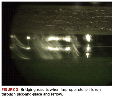
The integrated dispense head function also should be straightforward. Look for user-friendly software that offers intuitive prompts and guidance. Also, the dispense head should adjust for variations in the board surface. With dispensing, it’s critical that the z height of the needle is precise. If it’s too high, the adhesive will not wet to the board, causing the dot to be malformed. If it’s too low, the dot will not form the classic “Hershey’s Kiss” shape. The equipment’s ability to pinpoint the top surface of the PCB and compensate for any bow in the board is key to robust performance (Figure 1).
As you can see, designing a meaningful on-board, printer-adaptable dispense system isn’t simple. But, screen-printing equipment manufacturers have come a long way, and there are a few options now available. Adhesive dispense has been perfected and I suspect that robust solder paste dispensing isn’t far behind.
Clive Ashmore is global applied process engineering manager at DEK International (dek.com); cashmore@dek.com. His column appears bimonthly.
A look back at friends and colleagues who left us in 2009.
2009 came in like a bear and left like a lamb, but was felt deeply by all. Likewise, many of our friends and industry colleagues who did not make it through the year leave behind remarkable legacies and compelling memories. This month we reflect on their impact on our industry and our lives.
Dr. Carl Tautscher, 83, cleaning expert, author, and chairman of the IPC Cleaning and Contamination Control Subcommittee.
Jim Thiel, 61, cofounded Thiel Audio.
Richard (Dick) Schedtler, 60, vice president and owner of AR Marketing, and former Intel engineer.
Marty Jawitz, 78, former Litton Guidance and Controls engineer and author.
Velma J. “Val” Greig, 71, former auditor at Tektronix and Merix.

Dr. Steven Case, 60, founder and chairman of CyberOptics Corp.
Jerry Lee Cartwright, 51, engineer at Western Digital and Celestica.
Barry O’Brien, 56, late of Horizon Sales manufacturer’s representative, MidWest Circuit Products and Foundation Technologies.
Bradley Jay Black, 50, ex IBM, Celestica, and Ayrshire Electronics.
James (Jim) J. Miller, 76, product development engineer, Laminating Company of America (LCOA), BF Goodrich and Daubert Chemical.
Roy Matheson, 83, former production engineer at Sheldahl.
Scott Hudson, 52, semiconductor industry analyst at Dataquest, In-Stat, IDC and iSuppli Corp., and former staffer at Apple and Sanmina-SCI. 
Allan McKinnon, founder, rep company Allan McKinnon & Associates, and PCB wet process equipment manufacturer FSI.
Harvey Simonds, 48, former field service engineer at Vitronics-Soltec and service technician at Xerox.
Mark Shepherd Jr., 86, 40-year veteran in engineering and management Texas Instruments; was chief executive from 1967 to 1976 and chairman from 1976 to 1988.
An elegant solution to space and weight constraints, PoP requires specific handling techniques and profiles.
Solutions for packaging multiple die elements in a single package outline have evolved rapidly. Vertically stacking several semiconductor die on a single semiconductor package substrate proved efficient for a number of high-density memory applications. When mixing some newer multiple function processor and controller products with more mature, high yielding memory die elements, however, the overall package yield did not always meet expectations. A solution that has proved more efficient is a package-on-package (PoP) methodology designed to vertically combine fully packaged and pre-tested discrete logic and memory on separate array configured package substrate levels that are designed to align and mount on top of one another (see cover).
Package stacking is proving ideal for a variety of applications requiring greater functionality, higher performance and a smaller footprint: Stacking pre-tested package sections enables a high degree of flexibility for designers, permitting virtually any combination of memory to be combined with any logic chipset. Combining discrete logic and memory packages in this vertical configuration not only saves space on the circuit board, it typically reduces pin-count, simplifies system integration and enables enhanced performance. A number of products are already taking advantage of this multiple die packaging solution, including wireless handsets, digital cameras, portable game players, and GPS products.
Cellular handset designers in particular are faced with providing more features in smaller and lighter form factors. Because many stacked PoP memory products are furnished with a consistent footprint and pinout, users can easily configure variations that meet different product applications or incorporate new flash, SDRAM or other devices as they are introduced.
When the PoP device is furnished to the user pre-joined, the package can be mounted onto the circuit using conventional SMT soldering processes. These products are furnished as fully tested single package units. Some users will insist the sections be furnished as separate pre-tested packages ready for joining during the board-level assembly process. The latter version enables flexibility in system configuration and supply chain management. In either case, these devices are normally compatible with existing surface mount assembly process methodologies.
Whether the IC package sections are manufactured within a closed (in-house) environment or supplied from outside sources, quality and integrity of the end product is paramount. However, source and configuration control and material tracking throughout the life of the product are also a concern. Each package section has been electrically tested before PCB mounting, assuring users that multiple die PoP products will meet all performance criteria. Even when IC package sections are furnished by different offsite suppliers, the logic device supplier is responsible for assembly and test for the logic section, and the memory manufacturers are responsible for assembly and testing of the respective memory section.
The base package and top package units are furnished with alloy spheres compatible with most lead-free solder compositions. If users choose to perform the joining of the package sections during board-level assembly, they will need to consider placement machine flexibility. Depositing solder paste on a circuit board is most commonly performed using a stencil printing process, providing solder to all component attachment sites with a single process step. Mounting the upper section will require a different strategy, however. Due to the physical profile of the base package unit, depositing solder paste on attachment sites distributed on the narrow top edge of the base unit is somewhat of a challenge. Stencil printing solder paste at these contact sites is really not practical. Component suppliers have successfully adopted several alternative methods to accommodate attachment of the upper package section. This includes solder paste and flux paste dispensing at each contact site, solder flux-dip transfer and solder paste-dip transfer to the upper package section before placement on top of the lower package section.
Dip transfer process. A number of solder suppliers offer dip transfer-compatible solder paste. Indium, for example, offers a halogen-free material (Indium8.9-HF) in two alloy configurations: SnPb eutectic and SAC 305. Solder paste is applied to the spheres using a dip-transfer process. The material is systematically maintained in a shallow reservoir at a precise level using a doctor-blade mechanism. To monitor this procedure, newer generations of pick-and-place systems are equipped with bottom-focused digital cameras that, when programmed, can detect missing solder ball contacts or contact without the correct volume of flux or paste coatings. Typical PoP applications only require 25 to 45% of the sphere height to be coated with flux or solder paste. When solder paste is involved, care must be taken to avoid contaminating the bottom of the package itself with the fine-grain solder paste, as this may cause bridging defects.
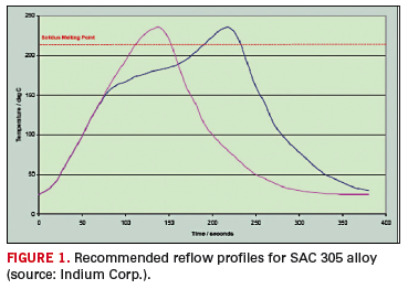
The peak reflow temperature will vary with the alloy type. Solder suppliers recommend a short preheat (140° to 150°C for SnPb37 and 150° to 160°C for SAC 305) for less than 45 sec. to reduce any solder balling caused by excess paste. Reflow solder profiles typical of those shown in Figure 1 should ideally be a linear ramp at 1 or 2°C per sec., up to 20° to 30°C above solidus temperature. The minimum time above liquidus should be 20 sec., followed by a rapid cool down to reach the solidus state.
A number of assembly systems available have been configured to accommodate 3-D package stacking and have included dip-tray stations between the package pickup location and the board. This feature was originally intended for flip-chip assembly processing, but works just as well for PoP applications (Figure 2). For optimum performance, the manufacturer recommends storing solder paste syringes and cartridges tip down at ≤10°C for maximum shelf life. Storage temperatures should not exceed 30°C for more than four days. The material should be permitted to stand for at least four hours at room temperature before using. Once removed from cold storage, the solder paste in a sealed syringe may remain at room temperature for up to seven days before and during usage. However, once outside the syringe, its working life is estimated to be no greater than eight hours, and may be less under high temperature (>25°C) and humidity (>70% RH) conditions. Further, the paste should not be subjected to multiple cold/heat cycles because viscosity can change and flux separation may occur. A number of materials have been formulated for no-clean applications, and can be left in place on the final package. However, when necessary, flux residues can be removed by using commercially available flux cleaner.

Post-assembly process evaluation. One of the challenges PoP device suppliers faced was managing the CTE mismatch and modulus variation of the dissimilar materials within a package. Although the PoP device will experience several levels of temperature exposures during assembly processes, the plastic-based components are expected to meet acceptable planarity and flatness requirements. The JEDEC 95-4.22 design guide document recognizes the relatively wide differences between the die element and resin-based materials used in the package assembly process. The standard, however, does not specifically define “flatness” criteria, but it does establish a parallelism tolerance of 200 µm for controlling the orientation of the top surface of the package with respect to the seating plane. The planarity limit of the seating plane contact features must be within 100 to 120 µm (depending on the ball diameter used). Even so, the tandem package configuration may be prone to some degree of package warp during the board-level assembly process, due in part to the physical variation between the resin-based multilayer circuit board material and the relatively thin resin-based package substrate materials. The primary concern is that if this warp condition is excessive, it can cause random solder defects that will compromise product reliability or prevent proper functionality.
Physical reinforcement. Many of the BGA-configured PoP products are targeted for the commercial wireless handset market. Because these handsets are subjected to various degrees of physical shock, vibration and thermal gradient extremes, some manufacturers of these products will physically stabilize the array packages with an epoxy resin underfill. The liquid underfill material is typically dispensed at the package edge and, by capillary action, flows under the device, furnishing a mechanical bond between package and PCB. Several different types of underfill are used. The most commonly used underfill compounds are referred to as snap cure, low profile, high performance, and reworkable.
To reduce voiding and ensure proper flow and adhesion of the underfill material, the surfaces of the PCB and package substrate must be free of flux residue. In addition, component suppliers warn that most materials used for both underfill or molding are sensitive to moisture absorption.
Substrate warping. Primary markets for the PoP devices are miniature portable products where package outline, profile height and package warp must be minimized. Substrate warping has plagued the multi-level package products throughout their relatively brief history. Manufacturers recognize the negative warp effect of the outer edge area of lower package interposer. During the package-to-board assembly process, if the base (or lower package) substrate flexes downward at its edge, the solder ball contacts mating with the host PCB can collapse to the point of merging together. Likewise, if the second-level package substrate warps in the opposite direction of the lower package, the solder interface will elongate and possibly separate.
Package assemblers have noted that most upper-level packages will have two or more die. The accumulated die thickness, along with the physical support of a high-temperature mold compound, considerably minimizes the warp condition. However, where the die element and mold compound on the lower package helps to minimize warping in its mid-section, the unsupported, relatively thin perimeter area is not restricted. This is the portion of the package that is configured to join with the upper level package and is more prone to warping.
Additionally, users expect future generations of PoP to furnish significantly greater functionality. Due to the increased complexity of the logic die elements and the demand for greater memory capacity, more contacts will be needed for both the upper and lower package sections. For many of these applications, OEMs would like to limit the outline to 12 x 12 mm (10 x 10 mm would be even better). The current JEDEC design guide standard defines a minimum contact pitch of 0.50 mm, allowing a maximum I/O for a 12 mm square configuration of 529, and only 361 I/O for a fully populated 10 mm square package. To meet the I/O density for the next generations of mixed function 3D packaging, many companies are anticipating the adoption of 0.4 mm and even 0.3 mm contact pitch.
Although widely used for single die wafer-level chip-scale package (WLCSP) and flip-chip applications, the finer pitch for an alloy ball or bump contact configurations on PoP applications are proving to be very difficult to manufacture. Some companies have found limited success by printing and reflowing solder onto the ultra-fine pitch contact sites, but profile uniformity of the contact features do not always meet the established criteria for planarity.
Avoiding the need for underfill is also a goal for many companies manufacturing products in high volume. Until this process stage, everything is running hands-free and smoothly through a series of conveyor transfer systems, from package placement to reflow and cleaning. The assembly is then transferred to a dispensing station for applying the underfill material and, for some materials, a curing cycle that could be as long as one hour. Add to that the detection and correction of any solder process defects or package removal and replacement may be difficult or not practical.
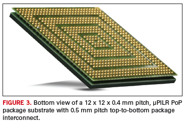
A viable solution has been developed to provide finer pitch and higher contact density for PoP applications. A unique substrate interposer fabrication process now available furnishes solid raised copper contact features for package stacking and board mounting in place of the ball contact features. This µPILR provides significantly smaller contact feature and finer pitch variations of 0.40 (Figure 3) down to 0.35 and 0.30 mm.
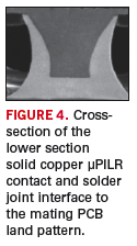
When comparing the µPILR contact profile to the more common solder ball connections, the contact geometry is significantly smaller in both diameter and height, enabling a much lower finished package profile. The solid copper core contact (Figure 4) is slightly tapered in shape and coated with a nickel/gold (ENIG) alloy that is compatible with either eutectic or lead-free soldering processes.
Assembly of the µPILR package-on-package device is very typical of most surface mount processes, beginning with solder paste printing, pick-and-place and reflow soldering. The stencil successfully used for printing is a 100 µm thick stainless steel foil with laser ablated 270 µm square apertures. Because of the very small stencil aperture, the recommended solder paste used for this application is a Type 5 powder size. Precise placement of the 0.40 mm pitch components is critical as well. When placing ultra-fine pitch array devices, machine placement accuracy should be in the range of +/- 20 µm to ensure a reasonably uniform solder fillet at all contact sites.
One of the benefits of the package substrate structure is the ability to reduce interconnect solder volume and tailor the solder shape to permit closer spacing of interconnects between package and board. An extended solder wetting plane provided by the package pins makes the µPILR less susceptible to solder defects caused by the warping typical of the BGA configured devices. Also, it does not require post-assembly underfill for mechanical stability or reinforcement. This is due to the solid copper pins providing crack stop reinforcement against solder fatigue cracks resulting from mechanical shock or thermal cycling. Reliability tests have shown the novel PoP to outperform the BGA PoP and exceed customer standards in drop testing and temperature cycling by 3 to 8 times without underfill.
Vern Solberg is founder of ST Madison; vsolberg123@aol.com. Phil Damberg is vice president, operations, interconnect, components & materials, at Tessera (tessera.com).
Effects of varied keep-out distances for 0201 and 0402 components.
The trend toward smaller chip components and finer pitches on IC packages means smaller volumes of solder paste are required on each pad if problems of tombstoning, mid-chip balling and bridging are to be avoided. However, in most of these assemblies, there are also large components that require substantial volumes of solder to form joints with the required electrical and mechanical properties. For some components and finishes, extra solder paste is needed to compensate for potential coplanarity issues. Given the constraints on the area ratio, if an adequate transfer efficiency is to be achieved, the extent to which the solder paste volume can be controlled by varying the aperture dimensions is limited.
While there is hope that alternative application methods will make it possible to optimize solder paste volume for each pad, for the time being, the most cost-effective solution is to use a step stencil in which stencil thickness is varied to fine-tune the paste volume to the requirements of the component terminations. This solution imposes a constraint on the layout to the extent that components with similar requirements for solder paste volume have to be grouped. However, a greater concern in assemblies, in which space is at a premium, is the “keep-out” distance required on either side of the step.
Large keep-out distances used to accommodate various stencil thicknesses represent a significant loss of area available for component mounting. In this first project of iNEMI Asia, the objective is to determine for a representative range of components what the minimum distance on each side of the step can be without compromising the quality of the reflowed solder joint.
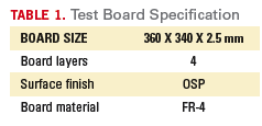
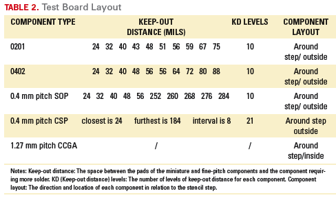
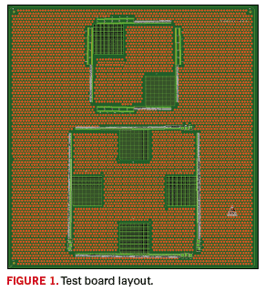
Test board specifications are listed in Table 1. The keep-out distance for step stencils has been described in IPC-7525. For the purpose of this project, boards were designed to provide a range of keep-out distances for 0201, 0402 and 0.4 mm pitch SOP and CSP components (Table 2). To assess the effect of printing direction, components were arranged around all four sides of the stepped area.

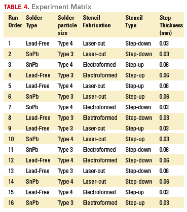
Experiment Matrix Design
Given the project objective of determining the minimum keep-out distance that can be used in practical application, the experimental program covers a range of process variables typically encountered in commercial production (Table 4).
Experimental Procedure
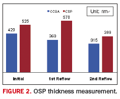
OSP thickness measurement. OSP finish solderability is known to be affected by the copper roughness and its ability to survive a reflow profile. It is known that OSP thickness may vary due to copper roughness. FIB was used to measure OSP thickness, since this method can accurately reveal the relationship between OSP thickness and copper roughness.
Figure 2 shows results of OSP thickness measurements on CCGA and CSP initially, and after the first and second reflow. The greater initial thickness of the OSP on the CSP pads is thought to be due to their smaller size. After the first reflow, there is not sufficient loss of coating thickness to compromise solderability, even on the copper peaks where the coating is thinner. After the second reflow, there is significant loss of coating thickness, but there is still sufficient coating on the peaks to protect the overall pad solderability, so that it is not expected solderability will be a factor influencing results in the later assembly stage of the project.
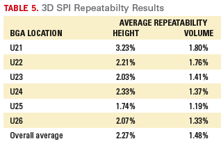
GR&R. GR&R was performed to determine the repeatability of the solder paste inspection equipment before starting the experiment. It was considered that results should be consistent within 10% of the measured value. A single board was printed and then inspected nine times, and the deposit height and volume results for BGA pads summarized in Table 5. The repeatability was calculated as follows:
Repeatability = 6 *σ/ (0.8 * average value)
Where σ = standard deviation of 9 samples
Average value = the average value of 9 samples
0.8 presents ± 40% process window
The repeatability was found to satisfy the set criterion (Table 5).
Printing parameter settings. Initial settings for print speed, squeegee pressure and separation speeds on a Speedline Accela printer were those recommended in the solder paste data sheet. Adjustments were then made on the basis of transfer efficiency, deposit shape and cleaning of the stencil surface, with the final settings listed below. To avoid any variation due to squeegee stroke direction, only the front to rear direction was used.
For runs 1-4:
- Print speed 75 mm/sec
- Squeegee pressure 8 kg
- Separation speed 5.5 mm/sec
- Separation mode Continuous
For runs 5-16:
- Print speed 35 mm/sec
- Squeegee pressure 8 kg
- Separation speed 5.5 mm/sec
- Separation mode Continuous
These settings were kept constant for all the remaining run orders (stencils) with careful checking of print quality after each stencil change. To enhance statistical significance, there were three repeats of each run order; a total of 48 boards were printed, with every pad inspected by 3-D SPI. Solder paste transfer efficiency and consistency were also recorded for analysis.
Data Analysis
DoE run. The DoE analysis was performed on each component surrounding the steps. These components are 0402, SOP, CSP, and 0201. The DoE analysis of 0402 is presented here as an example.
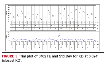
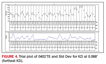
The 0402 component had 10 levels of KD. The closest, KD1, was 0.024˝. The furthest, KD10, was 0.088˝. Trial plots of 0402 data at each KD, grouped by DoE run order, orientation and side, indicate that ORT has a significant effect on TE (transfer efficiency) and deposit height, while the side does not have such a significant effect where:
- RO is run order.
- ORT is orientation of the component direction in relation to the step. ORT1 means the left and right side of the step, while ORT2 means the top and bottom side.
- Side is the side of the step. For example, ORT1 Side1 means the left side of the step.
Figures 3 and 4 are examples of such trial plots that represent the two extremes of KD. It can be seen that the TEs are almost the same for Side 1 and Side 2 for each run, but that there is a significant difference between ORT1 and ORT2 for most runs. This means ORT should be a separate factor, but the data of both sides may be able to be combined to simplify the DoE analysis.
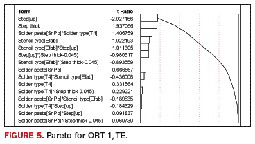
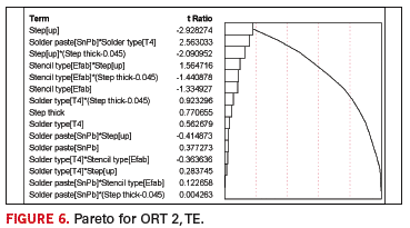
Among the five main DoE factors and the ten possible two-factor interactions, step appears to be the most significant factor in determining TE for both ORT1 (Figure 5) and ORT2 (Figure 6). The next most significant factors appear to be step height for ORT1 (Figure 5), and then solder paste and solder type combinations (Figure 6).
KD trend analysis. The line plot, which directly presents the trend for each run and differences between runs, was also used in the analysis of the results. Transfer efficiency and consistency will be particularly considered here, and results for 0402 are again used as examples.
Figure 7 shows the line plot of TE for 0402:
KD is not the significant factor in a single run, which means TE varies little with increasing KD;
TEs differ between some runs, especially Runs 13 and 14, which have TE values higher than other runs.
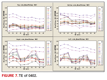
Figure 8 shows the line plot of transfer consistency for 0402:
KD is not the significant factor in a single run, which means TC varies little with increasing KD
TC differs little between runs, but Run 10 is an exception;
There is a large variation in TC for all 16 runs on the left of the step at 0.056˝ KD. The cause has been the subject of discussion by the project team and attributed to differences in the stencil fabrication.
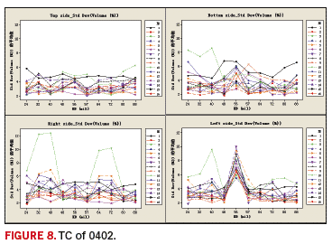
Table 6 summarizes the analyses of 0201, 0.4 mm pitch CSP and SOP components using this method.

First Stage Summary
Based on this analysis, the following conclusions have been drawn:
While it might be expected on the basis of common sense that the farthest KD should yield a better TE and deposit height than the closest KD, the trend analysis shows the KD has little or no effect on TE and height for 0402 and SOP type pads. Variations between DoE runs are greater than variation with the KD over the range studied.
For all keep-out distances and run orders, orientation has a significant effect. ORT1 (aperture at the side of step) always gives higher TE than ORT2 (aperture at the front/rear of the step). But with the same orientation, side has little or no effect.
From the overall DoE analysis, the project team saw the following factors as important:
- Solder paste type.
- Stencil type.
- Step down/up.
- Step thickness.
- That was expected, and confirmed the team had chosen the right factors and/or level setting.
An unexpected result was some DoE runs yielded TEs significantly different from others. The cause of this excessive swing in the response variable is unknown at this point; more investigation by the team is needed to understand and explain the cause.
Based on the results of the first stage printing experiments, assembly verification was planned. Finally the optimum keep-out distances for each component type in various applications will be obtained.
Acknowledgment
The authors appreciate the close cooperation between Huawei, Alcatel-Lucent, Speedline, Indium Corporation, IST, Cisco, Rohm & Haas, Nihon Superior, Celestica and iNEMI on this project, and extend their thanks to Photo Stencil and all the engineers involved for their great support.
The iNEMI Solder Paste Deposition Group is Shoukai Zhang, Huawei; Rita Mohanty, Ph.D., Speedline; Xiaodong Jiang, Alcatel-Lucent Shanghai Bell; Runsheng Mao, Ph.D., Indium; Chiko Yu, Integrated Service Technology; Chuan Xia, Cisco Systems; Keith Sweatman, Nihon Superior; Desmond Teoh, Celestica; and Haley Fu, Ph.D., and Jim Arnold, Ph.D., iNEMI.
How a maker of branded computer peripherals became our EMS Company of the Year.
December 2003. That’s the last quarter KeyTronicEMS failed to turn a profit.
For those counting at home, that’s 23 straight quarters of positive earnings. An enviable track record, considering the vast majority of the world’s EMS companies have been plagued with the manufacturing version of the H1N1 virus during the past 12 months.
Through the four quarters ended in September, KeyTronicEMS managed net income of $178 million and net profits of $1 million. While most of the Tier 1 to 3 companies saw revenues fall 20% or more during that period, KeyTronicEMS’s were down just 14%. Those figures are not going to blow over anyone at, say, its Washington state neighbor Microsoft, but for the EMS industry, they show remarkable financial consistency. Moreover, the company is carrying no debt, having paid down all outstanding loans during its past fiscal year.
KeyTronicEMS is an interesting blend. Founded in 1969, it’s been an ODM since before the term existed. After a near-death experience as it watched the average selling prices of its core keyboard products fall off the cliff, it today ranks as the top performer among Tier 3 electronics manufacturing services providers (EMS companies with annual sales of $100 million to $400 million).
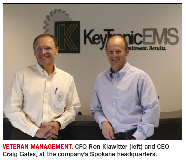
One sign of a well-built company is its ability to withstand changes in top management. KeyTronicEMS is undergoing just such a change now. The management team is transitioning to the next generation, as longtime president and CEO Jack Oehlke stepped down in April. He has been succeeded by Craig Gates, previously the company’s executive vice president and general manager, who has experience in engineering, marketing and sales in his 15-year tenure at KeyTronicEMS.
Surrounding Gates is a surfeit of experience, starting with CFO Ron Klawitter, who started with KeyTronicEMS in 1992; vice president of worldwide operations Douglas G. Burkhardt, whose tenure dates to May 1989; and vice president of engineering and quality Lawrence Bostwick, who joined the company in February 2006. (Gates and Oehlke’s relationship actually dates to Honeywell’s Microswitch division, where they worked together before joining KeyTronics.) Oehlke remains on the board of directors, however, and three other directors have been with the company since before the 2001-03 downturn. It’s an experienced group.
Markets served range from computer and industrial printers, telecommunications (satellite units, tracking devices and data transmission gear), and automotive and medical (diagnostic devices and sensors). It has a foot in the consumer market as well.
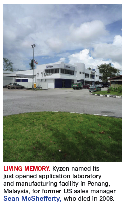
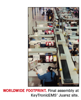
KeyTronicEMS has a staff of about 2,000 workers at five plants around the world, two each in the US and Mexico, and one in China. The primary domestic manufacturing site is a 140,000 sq. ft. building in Spokane, WA, which doubles as its headquarters. (It also has a 150,000 sq. ft. distribution center in El Paso, TX.) In Shanghai, it boasts a 63,000 sq. ft. high-volume SMT plant. Its largest sites reside in Mexico: the 375,000 sq. ft. Juarez campus, which houses four buildings and where some 85% of production takes place, and the 240,000 sq. ft. Reynosa facility.
KeyTronicEMS’s model marries ODM and EMS work, and the company was one of the first (and few) companies to successfully expand from original design and product development to contract assembly. The company’s genesis lies as reportedly the first independent supplier to make a PC keyboard for heavy-duty office use, and KeyTronicEMS has been granted almost 40 patents in high-end computer peripherals, specifically keyboards and mice. But keyboards now are a small fraction of its overall sales – less than $2 million a quarter. Yet the company persists because, as Gates says, it makes money.
“We look at it every year and it comes up profitable, so we keep doing it.”
In making the transition, in 1998, from an OEM to an EMS, KeyTronicEMS has beaten the odds. Many notable OEMs tried – and failed – to develop contract assembly units. Likewise, many EMS companies bought – and then shuttered – OEM operations. In fact, Gates calls the migration “a desperation move.” At the time, a turnaround group ran KeyTronicEMS. Its focus, recalls Gates, “was to be the last keyboard company standing.” However, PC keyboard ASPs were beginning to plunge (and have since fallen from about $60 to close to $3). “It was pretty clear it was not a business you wanted to be in,” he says.
It was the threat of that abyss that led then-CEO Oehlke, Klawitter and Gates to go into EMS. In hindsight, it seemed a natural move. Recalls Gates: “We knew we had a number of strengths: facilities in the US, China, and Mexico. We were vertically integrated; we had plastic moldings and PCBs. We knew how to get product from one spot to another. It was an overt decision.”
Still, the company eased into EMS. “One of the first contract programs was manufacturing a control panel for HP printers,” Gates says. “It looked like a keyboard – it had LEDs and components – but it wasn’t. We went from there to printers and other things. We were lucky or hardworking enough or smart enough to stay ahead of the decline in keyboards.”
Every company seeks success over the long haul, of course. Now in its sixth year of consecutive quarterly profitability, KeyTronicEMS sees itself as owning certain attributes unique to EMS companies in its size range. For starters, the geographical reach. With plants in China, Mexico and the US, it covers a lot of territory that few firms below Tier 2 can equal. Also, the three plants operate as if they were one. All three sites have identical equipment sets and processes. All production planning is performed from Spokane.
Although the program managers all reside in the Spokane plant, they command much greater responsibility than many of their peers. (Gates calls them “mini CEOs.”) Being grouped together, and in proximity to engineering, permits greater cohesion for loading and other decisions. KeyTronicEMS sees this as a meaningful way to appeal to its US customer base, allowing them to communicate in US time zones and with native English speakers, without long and frequent trips across borders or oceans. For their part, PMs directly reap the rewards when their business with a customer grows, giving them additional incentive to please.
“When volume expands, [our customers] don’t have to speak Spanish and go every week to Mexico and preside over a lot of intramural debates between facilities,” explains Gates. “We ensure the procedures are exactly the same in each place. [Customers] don’t really need to re-qualify the programs in each place.”
No losing quarters. The 2008-09 downturn affected everyone. That KeyTronicEMS managed to remain profitable throughout is remarkable. It lays credit not at the feet of any special oracle, but rather the experience of its management and its laser-like attention to the balance sheet. “I don’t think we saw it coming any earlier than anyone else,” says Gates. “We have a very scarred management team that has been through a transition few have made, going from OEM to CM. Those ups and downs taught us you have to have a very tightly managed balance sheet. When that downturn hit, we weren’t strung out for cash. Same thing on the inventory side. We have learned not to have a lot of cash tied up in inventory.” Indeed, as of the June quarter, its cash conversion cycle was 74 days, and inventory days were 69. Both figures compare favorably with Tier 2 averages, and easily best Tier 3 competitors.
Unlike most large EMS firms that react to downturns by taking large restructuring charges and inventory write-downs, leading to some horrific quarterly figures, KeyTronicEMS operates under the simple principle that it will not lose money, ever. Doing so, the company believes, makes customers squeamish and reverberates for months. “Even a quarter’s loss makes our customers nervous. It slows the sales process, and it makes them concerned there may be more problems coming,” Gates asserts.
“Our balance sheet, inventory and cost structure – all three are managed in a way that we hope we never have to lose money because we can be aggressive on all three levels. We also do a complete re-budget every quarter. I think that’s unique in our industry.”
Interestingly, Gates also credits years of ramping programs up and down. This background gave the company the chops to move product and people as needed, and in real time.
From a performance standpoint, KeyTronicEMS’s metrics are straightforward. One is 12% return on invested capital. Another is to beat its peer group’s revenue growth rate. When it misses on those goals, employees see it in their paychecks.
KeyTronicEMS has reached the $200 million annual revenue threshold almost on the strength of just 10 customers, all of which it has supplied since 1998. In that time, it has lost, according to Gates, “maybe two of any size, and both were by our choice.”
Adds CFO Klawitter, “Two or three years ago, the bulk of our business was from nine or 10 customers. The other 18 came over the last two years.” In fact, just before the recession, KeyTronicEMS was scoring several new customer wins, and points to its success there – 40% of its revenue in the past quarter came from customers of fewer than 18 months – as playing a major role in its near-term results.
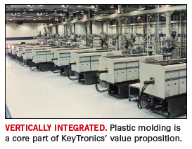
Its target customer program is in the range of $5 million to $30 million, too small to interest most Tier 1 firms. Yet KeyTronicEMS leverages its footprint, which includes a group in China that does most of its materials procurement, and vertical integration, which includes generous plastic molding capacity, with a responsiveness characteristic of Tier 3 firms. “We are of the size that we jump for our customers. If they were with a Tier 1, the customer wouldn’t get that kind of a jump,” Gates says.
“A lot of EMS companies’ costs are about the same. The differentiators come down to trust: Can the customer get the product when they need it to keep themselves in business? The people who understand that that is the core of a business relationship, those are the customers we want. Those who move every six months haven’t stopped to think about how much that costs them and us.”
Soft side. Every 18 months, all PMs, accounting, engineers and sales staff are trained on KeyTronicEMS’s EVA (Economic Value Added) philosophy, which looks at investments in plant space, equipment, working capital, and other operations, and reiterates the need for returns on investment. But in speaking with Gates and Klawitter, it is clear KeyTronicEMS is no Wall Street bank. Management keeps tight reigns on operations at all sites, often via video conferencing. Business reviews are conducted quarterly with the entire company, and management meets daily with all PMs and support functions, covering every program. “It makes it very easy to communicate how we are doing and tell our folks how their individual actions are going to affect their paycheck,” Gates says.
For a company that relies so much on understanding and quantifying its business, KeyTronicEMS reveals a certain touchy-feely side. Take its program managers. Before assigning a PM to an account, management considers their skill set and how it fits with the customer’s need. “There are some program managers who are former engineers and pretty much ‘0s and 1s,’ ” says Gates. “If you match them up with a customer who stresses more ‘feelings,’ it’s not a good match. It’s organic process, but key in making this work. The tight management and flatness of the organization and level of detail senior staff is exposed to on a daily basis is unique to our business and seems core to our success.”
Gates himself seems genetically predisposed to the term “we.” Almost insistently during the course of an interview with Circuits Assembly, he spread credit among his colleagues. The subtle gesture adds credibility to his comments, like when he says, “We are all involved in details. We have no patience for creeping functionalism. A number of us came from big organizations, and where you go wrong is when you think the function is more important than the organization. And we always remember where the money comes from. What really matters is how we treat our customers and how we work together to make money.”
For its unique but systematic approach to the electronics manufacturing services rollercoaster, and its stellar performance in all types of business environments, KeyTronicEMS is Circuits Assembly’s 2009 EMS Company of the Year.
Mike Buetow is editor-in-chief of Circuits Assembly; mbuetow@upmediagroup.com.
Migrating from manual to automated assembly and test.
Semiconductor companies pour millions of dollars into developing state-of-the-art chips like multi-core microprocessors, DSPs, FPGAs, ASICs, DRAMs and flash, among others. Semiconductor testing always has proven challenging. But as chips get more complex and smaller, the difficulties become even more apparent, both in cost and time. Successfully testing these advanced chips results in direct revenue for the company. Therefore, it often has high visibility from high-level management. That puts an enormous amount of pressure on test engineers to produce results, and they, in turn, rush their vendors, often pushing them up to and beyond their limits. As a result, extreme challenges are created for EMS firms involved in the assembly of ATE load boards.
A longtime industry practice exacerbates this issue. Previously, it was routine to manually assemble these boards, usually within a day or two, due to small order quantities. In the past few years, companies have been migrating to pick-and-place machines for better precision, accuracy and repeatability.
Although the assembly methods have evolved, standing expectations for turnaround time and pricing remain the same. Assemblers are pressured to quickly turn test boards and keep costs low, which proves difficult because of the tightly controlled processes involved. Manual assembly requires very little preparation, and its process is a lot more flexible in comparison. A typical pick-and-place/reflow assembly cycle is a few days due to a number of key considerations involved.
Test boards are bigger and thicker than regular PCBs. They are large, sometimes measuring up to 23˝ x 17˝, have anywhere from 22 to 42 layers, and are populated with thousands of components. They’re highly complex simply because they have to test innumerable chip functions, as well as simultaneously testing as many as 16 devices at a time.
A load board has a considerable amount of circuitry. That includes circuitry between components, as well as circuitry needed to connect to tester resources. Consequently, test boards tend to have considerably more gold and a high number of planes or metal innerlayers than conventional PCBs. Depending on the balance of these planes on a test board, and the board thickness, the board could draw a considerable amount of heat.
EMS providers are stepping in to move test boards to automated assembly. It’s not an easy path to forge. Test load board assembly has unique nuances and quirks that most assemblers may not properly translate.
That means having a good handle on correct thermal profiles, stencil cutting, pick and place, as well as understanding critical fabrication details.
Bill of Materials (BoM). Semiconductor test engineers traditionally generate the BoM from either CAD or schematic files. As a result, it’s not always in an ideal format to create the necessary programming at the assembler. In such cases, a general rule is flexibility, understand customer software capabilities, and work around them by taking the time to reformat the BoM. The trick is to do it accurately and still produce the intended result.
Like the BoM, auditing the parts kit for test board assembly is a bit different and should be handled gingerly, but expeditiously. Know what to question, when it’s important to ask, and when it’s not.
Semiconductor test engineers tend to expect the assembler to understand every nuance associated with their test boards, and these details will vary from one customer to another. That means they expect the assembler to know the parts to be used and any deviations needed. If every minor detail is questioned, it will delay the project. For example, if a BOM specs out a capacitor at a 5% tolerance, but the assembly house receives a better part with a lower one to two percent tolerance, they would normally consult the customer/OEM about using the lower tolerance part since it is a deviation from the BOM. The assembly process would be put on hold until the customer’s response was received. But that’s not so in the test world. It is extremely helpful for the assembler to learn which deviations are acceptable, specifically for a customer, and handle the issue quickly and accurately.
Thermal profile. Test board thicknesses can range as high as 0.187˝ to 0.250˝, with a high layer count that includes a number of ground and power planes, not to mention ample gold on the surface (typically 50 µ in of ENIG) on the tester and DUT pads.
The size of the board, along with the amount of metal it contains, places major challenges on developing a profile and arriving at the ideal temperature. Consequently, developing the correct thermal profile for a test board is very different than that for a commercial 0.062˝-thick, 12-, 14- or 16-layer board. Due to the sheer number of internal layers, considerable heat is required to bring the board up to a temperature for the solder paste to reflow. It’s important the heat profile is high enough for the paste to properly wet, while not so high that it damages the components or board.
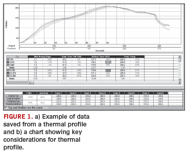
The challenge is to achieve the ideal temperature without burning the board or compromising the integrity of its various parts. Figure 1 shows an example of data saved from a thermal profile. It is normally archived with a job’s history in the event it needs to be referenced for future runs or to resolve issues. The chart shows key considerations when creating and defining a thermal profile.
Stencil. Cutting the proper stencil for solder paste application may seem minor, but the stencil plays a huge role in the success (or failure) of an assembly. For example, if an unusually small RF SMT component is involved, the stencil apertures must be accurately designed and cut to precisely accommodate it. Knowledge of stencil aperture patterns and their effect on solder reflow behavior is often overlooked. But if rework were necessary, it would defeat the purpose of moving the test board to automated assembly.
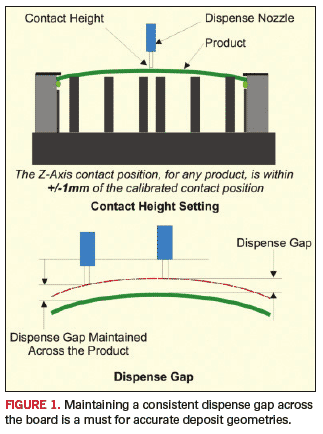
Also, if the stencil is not accurately cut, there can be dire consequences. For example, when running an improper stencil through pick-and-place and reflow, the result can be tombstoning and bridging (Figure 2). That can cause the board to undergo extensive amounts of touchup.
Placement. Some pick-and-place machines are not capable of handling test boards due to their rather large size. Therefore, it is important to audit the EMS provider’s equipment list for the proper placement machine.
Test load board customers are used to supplying small quantities of parts, usually in bulk or cut tape, and typically do not factor in part attrition. However, EMS companies require reels for pick-and-place, as well as an excess of components to account for part loss, usually expected with machine placement.
Moreover, setting up the machine requires files that weren’t necessary for manual assembly. Manual assembly can be performed with as little as a BoM (with its format not being an issue) and nothing more. Machine assembly requires a full set of files, usually Gerbers, IPC or centroid and X-Y data, and a BoM in a format that can be imported into the machine’s programming software. It is important for the EMS firm to convey these requirements to the customer before accepting and moving on with a project because customers may not be accustomed to providing, generating or acquiring these items if they have used only manual assembly.
Design for manufacturability is another issue the customer may not have needed to address with manual assembly. When a board is assembled manually, it is easier to work around DfM issues because a person can control and manipulate the part based on their observations. A machine will place a part based on the data it has been fed and cannot account for deviations, however subtle.
So to the customer, it may seem as if automated assembly introduces DfM issues, when in fact, those issues were already in existence, but not brought to his attention. The customer should be made aware that working around these DfM issues (as manual assembly would), may temporarily solve the problem, but is not ideal. The customer will benefit from DfM feedback because when addressed and resolved, the entire assembly process will be smoother and quicker.
Protecting the DUT. The device-under-test site (or sites) is the most important area of the load board. No matter how perfect the rest of the board is, if the DUT area is compromised in any way, the board can become useless. The EMS firm that is aware of this and pays attention to details can prove extremely valuable. For instance, nut fasteners (also known as PEM nuts) are often used to hold the DUT socket in place. To an average EMS, this may be a minor detail. An experienced EMS company will take great care to ensure the correct type nut is installed and that it is installed properly. Unlike other components on the board, a carelessly installed nut fastener sometimes cannot be repaired or reworked. If the PEM nuts on the board are not installed properly, the socket cannot be attached properly, which leads to not being able to load the DUT.
Protecting the DUT area while assembling a test board is a challenge (Figure 3). Most EMS firms use Kapton tape to protect areas on board during reflow. Kapton can sometimes leave a slight residue, which usually is not a problem with regular PCBs. However, DUT pads are more sensitive because Pogo or contact pins are used for board contact rather than conventional soldering. Because solderless pin contact is so critical, the DUT and test pads have to stay absolutely pristine during the entire assembly process – which EMS companies find challenging due to the number of process and people that the boards pass through. An experienced EMS company should be able to protect these vital areas from any type of contamination without hindering their normal assembly process. 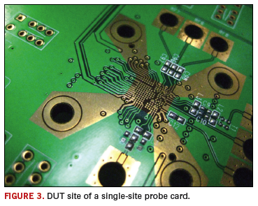
Board fabrication. Challenges are especially daunting for test board fabrication and certainly push the envelope. The high layer count of these boards means properly laminating 40 or more layers. The fabricator has to worry about tight impedance control, and because of the DUT package, these boards will often have blind and filled vias. ATE load boards also require stricter tolerances than what standard IPC guidelines dictate, and many fabricators cannot afford to accept and meet those tolerances. Although more fabricators are acquiring the experience, knowledge and equipment needed to build ATE boards, very few do it well.
Marilyn Ta is engineering program manager at Nexlogic Technologies (nexlogic.com); info@nexlogic.com.


