

Products
Squink desktop PCB printer now comes with Multilayer Package, a multilayer board option. Can inkjet-print conductive traces, dispense solder/glue and pick-and-place components on rigid or flexible substrates. Includes a new cartridge containing insulating ink and a curing lamp. The latter is placed on top of the circuit to cure insulating ink via UV light while protecting eyes and skin of users. Specially formulated ink is electrically insulating and compatible with existing Advanced Ink, and is printable on top of conductive traces or an insulating layer. Can also be used to improve printing on materials not easily compatible with advanced ink such as porous, stretchable or textile materials. Design using standard CAD tools such as Eagle, Altium and KiCad. Imports Gerber files.
BotFactory, botfactory.co
Quadra 5 offline x-ray is for 2D and 3D applications. Has 0.35μm feature recognition up to 10W of power, with optional 20W. Quadra 7 has 0.1μm feature recognition; comes equipped with two 4K UHD displays and 8 million pixels to show 50μm pixel pitch and 6.7Mp image size of Aspire FP detector. 4K UHD offers up to 4X detail compared to standard HD display screens and supports 68,000X total magnification.
Nordson Dage, www.nordsondage.com
Micro3Dslices produces superior laminography results and automatic analyzes the slice-by-slice images in less than 40 sec. per part. Uses virtual rotation axis to allow the region of interest to be chosen at any point on the large inspection area. Provides constant inspection results. For semiconductor and wafer inspection, 2D imaging and other inspection routines including QFN inspection.
Yxlon International, yxlon.com
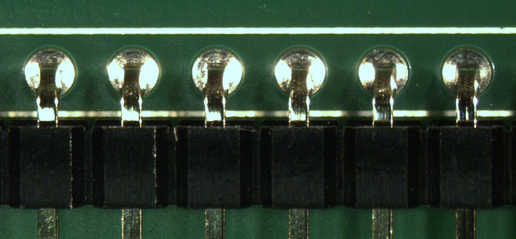
Tweezers Type meters including LCR-Reader now available with calibration fixture that conducts traceable calibration. Uses 14 known components of different types that lay within the applicable measurement ranges. When calibrated device is connected and activated, fixture connects to a different component which the calibrated LCR-meter or LCR-Reader measures, with results appearing on the meter's display which are then compared to the known values of the component. Two calibration fixture versions available: 4-wire or 2-wire connections. Is less sensitive to parasitics on fixture's PCB and measures values that previous calibration fixture could not.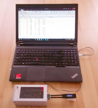
Siborg Systems. lcr-reader.ca
Universal Permalex Holder and Blade Assembly is now available for large format HIT printers. Comes in four standard colors: blue, silver, red and green. Is lightweight and includes sliding and floating paste retainers to increase SMT printer performance by keeping the solder paste neatly contained within the print area.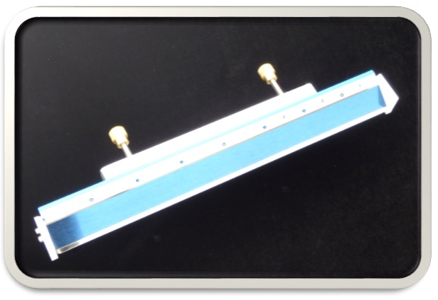
Transition Automation, transitionautomation.com
Slimline label feeder is 30mm-wide and has a teach-in function, counter, adjustable failure indicator, selectable trigger, and adjustable speed. Empty liner material is collected in a waste box. Is said to provide 50% space savings in a pick-and place-system.
Elite Feeder Solutions, www.elitefeedersolutions.com
EO-B series hand- and dip-soldering fluxes are alcohol-based and range in solids content from 1.8% to 3%. Are designated ORL0 or REL0. Meet DIN EN 61 190-1-1 with L0 classifications for corrosion behavior, halogen-free, and surface resistivity of uncleaned flux residues. EO-B-001 has very good process properties during hand soldering; EO-B-002 and EO-B-003 are for wave and selective soldering; EO-B-004 low solids flux is for all soldering methods and ensures minimal residues and clean appearances. EO-Y flux is not based on pure alcohol but on a mixture of alcohol and water. 
Emil Otto, emilotto.de
Fox SMD automatic placement system has a footprint of 88 x 109cm; weighs less than one metric ton. Consumes less than 750W of power, uses single phase voltage (230V), and recuperates energy from the motion system. Places components from 0201 to 33 x 80mm; dispenses solder paste and SMT glue. Accepts 180 intelligent feeders. Is compatible with Essemtec’s previous feeders. Places components at 4500cph (IPC 8950A) with an accuracy of 60µm. Board sizes are 300 x 400mm; component height is 30mm. Has an 18" touch screen. Runs on ePlace software.
Essemtec, www.essemtec.com
AutoVision machine vision software enables a barcode reading suite consisting of four smart cameras that adopt the machine vision toolset for Auto ID+ applications. Offers full library of software capability reportedly on the smallest hardware design ever in smart camera design. Fully adaptable to any barcode reading or machine vision application; can choose single smart camera with ideal footprint, industrial rating, and connectivity. Can choose software interface with capabilities to compliment needs of an application, from basic barcode reading to advanced measurement, gauging, and inspection. New software features include tools for color ID, spot-checking against stored colors, and counting or checking presence of certain colored features, such as on packaging or test tube caps; circle measure tool; enhanced locate tool to find multiple features of a part at once and inspect the integrity of a part based on relative locations of features.
Microscan, www.microscan.com
EO-G-001 water-based flux for selective soldering is halogen-free flux and meets all criteria under DIN EN 61190-1-1 and ISO 9454 for surface resistance. In tests, flux propagation area is less than that of alcohol-based fluxes tested, while rise-through and pad wetting were not adversely affected and soldering results were more than satisfactory. Cleanliness was as good or better than alcohol-based fluxes. Is classified OR/L0 under DIN EN 61190-1-1 or type 2.1.3.A under ISO 9454.
Emil Otto, emilotto.de
Dualbond LT2216 dual-curing adhesive, for electronic and optoelectronic automotive and consumer applications, reaches full strength within 90 minutes at 60°C after prefixation by light.
ML-5120A 120W direct diode laser (DDL) welder for soldering and plastic welding has low power consumption and high efficiency. Features localized heating for small parts welding and manufacturing applications with space limitations. Comes with temperature control function, which requires a separate dedicated unit to control laser output power. Directly applies light emitted from laser diodes (LDs) for thermal processing– without passing through a lasing medium, such as Ytterbium (Yb)-doped fiber or Nd:YAG (neodymium-doped yttrium aluminum garnet). Generates an invisible IR wavelength of 915nm. Small spot diameter of 0.2 millimeters enables fine soldering in small areas as well as high-density, small-pitch areas. Equipped with power monitor as standard equipment.
Amada Miyachi America, www.amadamiyachi.com
