

Taking a middle ground is verboten to avoid assembly problems.
Stencil design calls for three main criteria. One, the stencil should be completely flat because it needs to evenly distribute the amount of paste on all sides of the board. Two, it should be able to control solder paste spillage. If solder paste is spilled on an adjacent pad (or ball, in the case of a BGA), it could cause a short. Three, the stencil must provide optimum stability, meaning it can be repeatedly used without any issue. This could be achieved by using framed stencils versus unframed ones.
Stencil definition and design accuracy take on even greater significance when a high-count layer board is involved. In such instances, thicker boards are used for a load board application, for example, and unlike a standard six-to-12-layer commercial board, this thicker board has 20 or more layers, with more power and ground planes. This means a different thermal profile.
Stencil accuracy has a direct bearing on the thermal profile used on such a board. A thicker board, with a number of ground and power planes, requires considerably more heat for proper soldering. Also, for the same type board, a less accurate stencil design means too much or too little solder paste deposited, resulting in opens or shorts.
When a stencil is properly designed and solder paste is correctly deposited, the result is perfect printing. Put another way, this means few to no bridges or solder issues and little touchup and rework.
Special attention must be paid to devising apertures for surface mount pads on mixed signal PCB designs – in which one segment of the board is heavily analog laden, and the other digital. An analog segment requires a lot of heavy current and grounding. A thicker 0.006˝ to 0.008˝ stencil is recommended here. The thickest stencil would probably be 0.006˝ with a ratio of 1.1:1. The ratio of 1.1:1 means 10% more paste deposited compared to the pad size, thus providing a good fillet. A good fillet means enough solder is deposited, but not so much as to create a short (Figure 1).

By its nature, the analog section is a heavily ground poured area. Since heavy current is characteristic of analog circuits, those components must have extremely solid connections, either through the component side or bottom side, or internally through the ground plane. In this instance, paste deposition is called a “solder brick” (Figure 2), which describes how efficiently paste is poured on the surface mount pad. Also, a stencil for a mixed signal board must have isolation islands created to segregate current and voltage between analog and digital circuitry.

The digital side of a board with fine-pitch devices such as BGAs, µBGAs and QFNs, for instance, is another story. This calls for a ratio for paste deposits compared to the pad size of less than 1:1: for instance, a ratio of 0.9:1, which means 90% paste is being deposited. Put another way, 10% less paste is being deposited compared to the pad because the pitch is so fine. Care must be applied here because the balls of a QFN or BGA are so close that too much paste can cause a short between them.
Step Stencils
A step stencil, characterized by its different depths, is used when the application has a considerable number of analog components on one side of the board and a lot of digital on the other side. In other words, it requires different amounts of paste dispensed on different segments of the board. It provides additional paste height in certain PCB areas, and in this case, it’s called a “step-up” stencil. Conversely, sometimes, it provides lower paste height in certain PCB areas; thus, it’s called a “step-down” stencil. In other instances, where the PCB has raised areas, a “relief step” stencil is used.
As an example of a step-down stencil, consider a board with a 0.020˝ pitch QFP. A 0.007˝-thick stencil is needed for resistors, capacitors, inductors and other passives. A step-down 0.005˝-thick stencil is then used for fine-pitch technology (0.020˝) SMT devices.
A step-up stencil is used not only for analog, but also for column grid areas (CGAs or CBGAs). For example, a 0.006˝ stencil is used for capacitors and resistors. However, a step-up 0.008˝ stencil is used for CGAs or CBGAs. The extra paste height is required to support those column grid areas because they require much more paste deposition, compared to the regular SMT components on the board.
Laser-cut step-up and step-down stencils provide ideal solutions for ceramic BGA and RF shield applications. In these cases, additional solder paste deposition is required, meaning solder paste brick height is higher. As a result, it deals extremely well with non-coplanarity issues. For instance, coplanarity typically becomes an issue when an RF shield is created using HASL, rather than gold, as a surface finish on the board (Figure 3). But it’s not that much of an issue in analog or an RF board side, because the more paste deposited, the better the solder joint, especially when digital circuitry is minimal.

Thus, ceramic BGAs are one of the applications for step-up, step-down stencils. Electropolishing and then nickel plating are recommended for those stencils to achieve a good paste release for smaller aperture sizes. This stencil costs more because more processes are involved, and electropolishing or nickel plating can mean longer turnaround time.
First-article inspection is a next critical step to verify the stencil design after solder has been deposited. At this point, a determination needs to be made whether sufficient paste has been deposited for an ideal solder joint connection. Also, first-article verification step involves paste height inspection for component pre- and post-loading. Even when component placement is completed, first-article inspection should be deployed at post-placement of components. Component pre-placement inspection is performed when there’s only solder paste on the pads to verify the correct amount of paste dispensed. However, post-placement is performed when SMT components have been placed to ensure correct placement and orientation.
In some instances, the EMS provider may take a middle ground for stencil design to minimize the probability of assembly problems. Issues arise in cases like this. Let’s say the PCB layout engineer keeps the benchmark on the digital side. Based on this design, adequate paste will be deposited on pads on the digital side of the board. But it won’t be enough on the analog side, thus creating voids.
Again, as mentioned, analog requires a 0.006˝ to 0.008˝-thick stencil, while digital needs a 0.004˝ to 0.005˝ stencil. Using the wrong-sized stencil negates the concept of step stencils – to deposit the precise amounts of paste on the analog side. Also, when taking the middle ground – for example, using a 0.006˝-thick stencil for both types – the digital side may get too much paste deposition, thus creating shorts, especially when finer-pitch QFNs or µBGAs are used.
Misregistration Causes
Paste misregistration occurs for multiple reasons. The following are the most prevalent. First, the stencil aperture opening doesn’t align with the PCB. This sometimes occurs during CAM, where the proper aperture openings are not created, resulting in paste misregistration.
Also, if a PCB layout engineer is not alert or careful, they may not view the component properly to see where paste needs to be dispensed. Therefore, a layout and design engineer has to be vigilant at reading the datasheets and reviewing the component specifications.
When special components are used, it’s not always clear as to what goes on the board and what does not, or what is masked. To design proper stencils, the PCB designer has to look carefully at the physical component to ensure aperture openings are correctly defined.
Using an unframed stencil is another possible reason for misalignment. After an unframed stencil is placed on an adapter, but before it is mounted on the printer, is where damage can occur, and human interaction creates reliability issues. Also, a cleaning process must be extremely accurate during and after printing. If a stencil isn’t properly cleaned before it is archived, paste residue may be left on the apertures.
Zulki Khan is founder and president of Nexlogic Technologies Inc. (nexlogic.com); zk@nexlogic.com.
Companies return to market with new requirements, fresh capital, and new ways to evaluate cost-of-ownership.
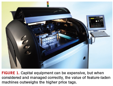
Value can be defined in many ways. In a financial sense, value is how much of what you need you actually get for your money. But measuring “how much you get” is not straightforward. It’s easy to confuse cost with value. Low cost does not automatically translate to the best value. Likewise, the highest price isn’t necessarily the best value. The purchase price of a capital item is only one element of value, but it can be one that is disproportionately influential in the purchase decision. A useful automotive analogy can be drawn here.
For most individuals, a car is among the largest capital purchases, or investments, they will make. Will the cheapest car represent the greatest value? The costs of running and maintaining a car need to be taken into consideration to determine a better measure of value. Then there’s the issue of the value of the car when the owner has finished with it. Leasing companies know this because their long experience and amassed statistical data have turned whole-operational-life value into a science. It’s why the monthly lease price of different vehicles is not directly proportional to their forecourt purchase price.
In principle, the same is true in industrial capital equipment. But all too often, the potential end-of-life value of a capital purchase is not taken into account. Could it be because it’s more difficult to identify the use to which the equipment may subsequently be put? Or perhaps because there’s no guide to look up the likely fiscal worth of used equipment? The experience of most electronics assembly capital equipment vendors is that investment in new equipment is typically justified on the basis of a single manufacturing requirement or contract, or at least an identifiable operational run lasting a few months to a couple years. Equipment needs to pay for itself easily within a percentage of that period to deliver a financial return. Understandably, the shorter the identified operational run, the more critical the initial purchase price of equipment seems to be to the purchase decision. But often this is a false economy.
A few years ago, one of the industry’s leading surface mount pick-and-place equipment vendors ran studies into the equipment investment its larger EMS customers were making as a proportion of its total outlay to resource each new contract they secured. The result was usually around 2.5%. (The largest single portion of every contract investment was the procurement of components.) Within a typically conventional SMT assembly line comprising printer, placer and reflow oven, the placement machines invariably represent the largest part of the investment – accounting for around 1.5% of the 2.5%. Allowing for the oven, this means less than 1% of the total investment goes toward the screen printer. At less than one-hundredth of the overall investment funding, a few percent variation in the purchase price of a screen printer is relatively insignificant compared to what return the right equipment can deliver – or the horrors of what it may cost if it doesn’t deliver.
Which is why, for these large EMS companies, the value of the printer – measured in terms that include less tangible elements like on-time delivery, service support responsiveness, applications expertise, fast ramp to productivity, maximized uptime, etc. – is always more critical than the initial machine cost.
Not all screen-printer users are large EMS providers after lucrative new contracts. But all manufacturers can improve printer ownership value by considering a few strategic points when specifying the equipment.
‘Flawless balance’ challenges. Screen-printer productivity is a combination of throughput and yield. Conveying the maximum number of good printed boards from the print platform to keep downstream processes operating at peak efficiency is the productivity goal. But getting a flawless balance between throughput and yield is a challenge; there’s no point in speeding the print process if yield suffers. Screen printing still has the most potential of any process in the assembly line to introduce catastrophic faults.1,2 A single unprinted pad, if undetected, can render a subassembly useless or incur significant cost in diagnosis and rework. Or both.
The temptation to ramp throughput by, for instance, reducing cleaning cycle frequency or increasing squeegee excursion speed can lead to lower yields as the process moves out of control. So many variables influence the process that deploying expert knowledge is the best way to keep control. Dr. Ron Lasky of Dartmouth College, a leading Six Sigma process expert, illustrates aspects of process control in the screen-printing domain using a fictional process expert (“The Professor”) who investigates manufacturing issues, and who – as a profit sleuth – often focuses on COO as he helps electronics assemblers recover lost profit.
In one of The Professor’s investigations,3 Dr. Lasky cites the overall losses incurred by a manufacturer from switching to a cheaper solder paste. The production engineering manager’s expectation is to save more than $30,000 per line per year by using paste costing only 5 cents per gram, as opposed to 8 cents per gram.
But the paste has one property weakness in the form of lower on-screen open life, so each board printed after a stoppage must be cleaned and reprinted because the paste has “stiffened” – an exercise that costs 20 minutes in lost production per line per day, and which, with the production run figures in the example, results in a cost burden of over $340,000 per year. It’s presented as fiction, but the impression is that it’s not. In any event, it illustrates exactly the kind of process variable that requires specialized expertise to fully evaluate and manage.
Operational cost-of-ownership. Another obvious way to reduce, or at least contain, the cost associated with running a screen printer is to ensure the system is paying its way all the time – or as close to that as is practical. Downtime is the enemy of productivity. And productivity often relates directly to profitability.
Downtime comes in many forms, most predictable and therefore manageable. Even unscheduled stoppages often result from operator oversight or error, or from a process or material issue, and in theory can be legislated against.
Scheduled stoppages for consumables replenishment and planned downtime for maintenance are both areas worthy of scrutiny. Choosing a printer that has fewer maintenance intervals, or that offers easier access to permit maintenance to take place faster, will render it offline for less time, which equates to better value when measured in terms of productive uptime. Solder paste replenishment is a frequent and necessary intervention, so rapid and easy access to the print area that lets this procedure take place more quickly has a true value that reduces COO by keeping the printer productive.
In addition, simple actions like selecting the optimum consumables for production needs can improve productivity. A recent study of understencil cleaning fabrics reveals not only measurable differences in the cleaning effectiveness of materials, but disparities in the length of the fabric rolls for a given price.4 Naturally, the longer the roll, the less often the printer will need to halt for replenishment. Equipment manufacturers may offer a number of equipment options on printer platforms that mitigate stoppages, from effective cleaning fluids, fabric rolls and operator alerts to sophisticated tools such as paste height monitors and high throughput understencil cleaning.
The latter is a case in point on the issue of cost versus value. Newer generation systems have cleaning excursions that take half the time, use less than half the quantity of understencil cleaning fabric, and clean more effectively than comparable systems. They offer a choice: clean to the same standard as before, which means less frequently but more quickly to dramatically increase batch throughput by reducing the number of times the printer halts for a cleaning cycle and shortening the time it takes when it does; or clean as frequently as before, but twice as fast, to really safeguard yield and increment throughput. Clearly, both strategies have a tangible productivity value.
Another constraint on maintaining productivity is in high-mix assembly environments with high product changeover. Identifying ways to reduce the time it takes to set up the printer for a new board is key to productivity when measured over several batches, a more realistic snapshot of production. Using The Professor’s technique of calculating potential earnings when the printer and line are running to capacity determines revenue lost for every minute of downtime. Again, tools exist to assist. Small EMS providers and OEMs that run several products in short batches should look at automated tooling for board support; at self-loading and aligning stencils to speed the operation and eliminate operator errors; and be aware of the time it takes to upload or initialize the software print file.
Looking at these stoppage types prompted Dr. Lasky to articulate how a simple cocktail of screen-print process considerations can reverse an expected financial outcome. The example is a manufacturer who contemplates deploying new screen printers with a purchase price $20,000 lower than those traditionally in use onsite; the intention being to save a total of $1 million over 50 lines. The Professor’s investigations reveal how tiny time-based procedural issues that appear insignificant on their own can wipe out capital equipment purchase savings. In the example, factors such as 10% longer changeover due to more steps in setting up board support, computer programming and stencil installation, plus 15% more time to replenish solder paste, result in 3% less production, producing 3% less product, which equates to 6% less profit. On lines intended to average $4 million per year in profit, the small stoppages accumulate to lose around $240,000 per line per year, making the $20,000 saving on purchase price a gigantic false economy.
A final COO domain has traditionally remained unfulfilled. Arguably one of the greatest potential COO gains to be made is in the ability to redeploy a screen printer from production runs to other uses. Thanks to platform concepts, screen printers can be redeployed, often with no more than a modest investment in a module to reduce cycle time by two seconds, or an inspection system for traceability and higher yields.
References
1. J. Pan, et al., “Critical Variables of Solder Paste Stencil Printing for Micro-BGA and Fine Pitch QFP,” IEEE/CPMT International Electronics Manufacturing Technology Symposium, 1999.
2. K. Feldmann and J. Sturm, “Closed Loop Quality Control in Printed Circuit Assembly,” IEEE Transactions on Components, Hybrids and Manufacturing Technology, Part A, vol. 17, no. 2, 1994.
3. R. Lasky, “ ‘Paste is Paste’: The Professor Hits the Road,” Circuits Assembly blog, Oct. 25, 2009.
4. C. Ashmore, “Understencil Cleaning’s Little Devil,” Circuits Assembly, August 2009.
Trevor Warren is Americas product manager at DEK (dek.com); twarren@dek.com.
Although final performance is measured in the time domain, a detour may be the faster route to a signal integrity solution.
Do you speak frequency domain? Especially if you are a digital designer, you should consider learning the language of the frequency domain. The time domain has special significance because it is the real world. This is the domain in which we live our lives, where we build our intuition, and where we measure digital performance. If the time domain is the real world, why would we ever want to leave to enter the frequency domain?
For signal integrity problems related to lossy transmission lines, working in the frequency domain can often help us find solutions to eye closure problems.
Sometimes, taking a detour through the frequency domain can bring an acceptable answer more quickly than staying in the time domain.
In this brief introduction to solving problems in the frequency domain, we will look at how to improve signal quality in high-speed serial links like PCI Express (PCIe) by speaking the language of the frequency domain.
Rise time in the frequency domain. If the time domain is the real world, what does this make the frequency domain? The frequency domain is not the real world; it’s a mathematical construct. As such, it has certain very special rules that must be followed. One rule is that only sine waves can be used to describe signals.
Each sine wave is described by a frequency, an amplitude and a phase. While the phase of a sine wave is important, we usually focus attention on the amplitude of the sine wave.
Any waveform in the time domain can be translated into the frequency domain using the Fourier Transform. While it is important to have done a Fourier Transform by hand at least once in your life, after that, it’s usually more important to get the answer as quickly as possible. Every version of SPICE can perform a Fourier Transform of any arbitrary time domain waveform.
The hidden assumption with these translations, typically called a Discrete Fourier Transform, or DFT, is that the waveform in the time domain is repetitive. The repeat frequency is either the clock frequency or the total simulation time. The repeat frequency has special significance. It is the lowest frequency that will appear in the spectrum and is called the fundamental frequency.
Every frequency component that appears in the frequency domain is a multiple of this fundamental and is called a harmonic. The collection of all the harmonic components is called the spectrum.
A very important waveform in the time domain and the frequency domain, to which most other waveforms are compared, is an ideal square wave. In the time domain, an ideal square wave has a zero psec rise time and a 50% duty cycle.
Its spectrum has three important features:
- Only multiples of the fundamental appear.
- The harmonic of each component drops off like 1/n, the harmonic number.
- The even harmonics, i.e., 2d, 4th, 6th, etc., have zero amplitude.
For an ideal square wave, the frequency components continue with their pattern to infinite frequency, always dropping off inversely with frequency or harmonic number. But, if the rise time is finite, this is not the case. After some frequency, which we call the bandwidth, the amplitudes of the frequency components drop off much more quickly than 1/f for an ideal square wave.
Figure 1 shows a 1 GHz ideal clock square wave spectrum and the spectrum of a clock with a rise time that is 5% the clock period. The relationship between the 10-90 rise time, RT, and the bandwidth, BW, is roughly approximated as BW = 0.35/RT. For this example, we would expect the bandwidth to be about 0.35/0.05 = 7 GHz. This is about where the amplitude begins to drop off below the ideal square wave spectrum.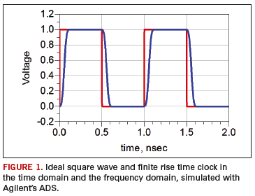
Every frequency component of an ideal square wave is significant in contributing to that 0 psec rise time. However small the amplitude may be at very high frequency, it is still important. Remove any and you won’t get the 0 psec rise time.
When the frequency component of a real waveform has an amplitude significantly smaller than the equivalent ideal square wave, it won’t be large enough to contribute to the rise time and can be ignored. The bandwidth of a real waveform is the highest sine wave frequency component that is significant. Decrease its bandwidth in the frequency and its rise time in the time domain will increase.
A fundamental measure of the rise time of a signal in the time domain is the frequency at which the harmonics begin to drop off more quickly than 1/f. For this reason, the bandwidth is often referred to as the knee frequency. The lower the knee frequency in the frequency-domain, the longer the rise time of the signal in the time-domain.
Signal propagation on real interconnects. How do real interconnects like traces on a circuit board, or coax or twin-ax cables, affect signals? In the time domain, we can evaluate the behavior of a single bit as it propagates down a transmission line. Figure 2 shows what a single 1 bit would look like traveling down a 0.003˝ wide FR-4 transmission line for a 1 Gbps signal, initially, after 30˝ and after 60˝.
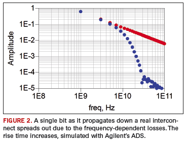
The single 1 bit starts out with a 1 nsec unit interval, and a very fast rise time. As it propagates down the transmission line, the wave form is dramatically affected. That single bit spreads out into adjoining bits. This cross talk between one bit and other bits is called inter-symbol interference or ISI. It contributes to the collapse of the eye. Figure 3 shows the received eye of a pseudo random bit stream (PRBS) signal at the three locations above.
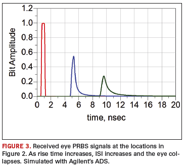
How the single bit spreads out is a very important metric of the behavior of the interconnect. Yet, as viewed in the time domain, the exact shape of the pulse is complicated and difficult to describe in a simple way.
Here is where the frequency domain description offers a simpler description. The term that describes how a sine wave differential signal is affected by an interconnect when it exits is the differential insertion loss, sometimes referred to by its S-parameter designation, SDD21. This is also called the transfer function of the interconnect. This measureable property describes what a sine wave with amplitude of 1 looks like when it comes out the transmission line. The differential insertion loss for these interconnect paths is shown in Figure 4.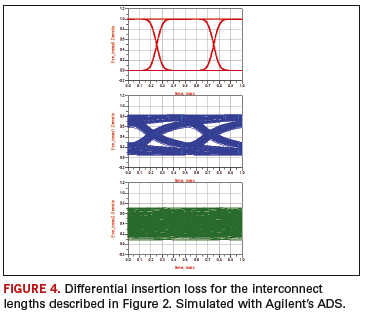
Every single interconnect has a similar SDD21 response. The amplitude coming out is always less than the amplitude going in, and the amplitude of SDD21 drops off with increasing frequency. On a log scale of amplitude, measured in dB, the differential insertion loss generally drops off nearly linearly with frequency. A metric of the dB/inch per GHz is one single number that characterizes most interconnects.
If we send an ideal square wave signal into a real interconnect, its spectrum will be multiplied by this transfer function. The SDD21 tells us how each frequency component will be attenuated. Higher frequencies get attenuated more than lower frequencies. This pushes the knee frequency of the signal’s spectrum to lower frequency, and increases the rise time of the signal.
This frequency-dependent attenuation of typical interconnects will cause rise time degradation, which will smear one bit into adjacent bits, result in ISI and cause collapse of the eye.
It’s not the attenuation of the interconnect that degrades the rise time; it is the frequency dependence of the attenuation. After all, if we take all the frequency components and just attenuate each of them the same amount, we will still have the same spectral shape of the bit sequence coming out. The frequency at which the knee occurs will be unchanged; the rise time of the signal will be unchanged, and there will be no ISI and no collapse of the eye.
Fixing the eye collapse in the frequency domain. We can fix the ISI in real interconnects by either flattening the insertion loss curve of the interconnect, or by changing the spectrum of the signal going into the interconnect so that when it comes out, it preserves the 1/f shape.
Designing an interconnect with a flatter response is tough. The root cause of the frequency-dependent loss is the combination of the skin depth dominated copper series resistance and the laminate material dielectric loss. For example, certain Gore cable assemblies use a very thin signal conductor, which has a frequency-dependent resistance much flatter than a typical copper core cable.
Likewise, laminates such as Rogers’ RO4350 have a lower dissipation factor and a flatter response dielectric loss curve. Both these interconnect design features reduce ISI with a flatter differential insertion loss response.
It is also possible to flatten an interconnect’s transfer function by adding some extra frequency-dependent gain at the receiver. If the interconnect has more attenuation at higher frequency, why not add gain that increases at higher frequency to compensate and flatten the overall response? Figure 5 shows how this works.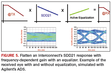
When we add frequency-dependent gain, we equalize the response of the interconnect across a wide frequency range. We call this process equalization. The ideal equalizer has a gain curve that is the exact inverse of the attenuation curve. With a flat response, the spectrum of the transmitter is preserved at the receiver; the knee frequency is the same as the transmitter; the rise time is the same, no additional ISI and no additional collapse of the eye.
Finally, the spectrum of the signal at the transmitter can be pre-distorted to add extra high-frequency components. The interconnect will attenuate the high-frequency components anyway. If we add extra high-frequency components at the transmitter, by the time they travel through the interconnect, they will be attenuated away, leaving the 1/f spectrum of a short rise time signal. The shorter the rise time, the less the ISI, and the lower the eye collapse.
One way of implementing adding high-frequency components is called pre-emphasis. Wherever a 1 bit begins, extra energy is added. Likewise, we could obtain the same pre-distorted spectrum by taking out low-frequency amplitudes. Whenever there is a string of more than one bit with the same value, reduce the signal level. This is called de-emphasis (Figure 6).
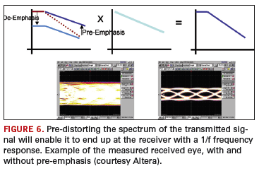
Both pre- and de-emphasis result in the same distorted shape in the transmitted signal spectrum. When either of these distorted signals travel through an interconnect, if optimized for the interconnect, the signal will come out the other end with a short rise time, less ISI and a more open eye.
By looking in the frequency domain, we can see how the techniques mentioned manipulate the frequency domain spectrum of the received signal. We engineer it to look more like an ideal square wave’s spectrum and recreate the shortest rise time to minimize its ISI and keep the eye open so that each bit can be detected as its true 0 or 1 value.
Even though final performance is always measured in the time domain, sometimes detouring through the frequency domain may be a faster route to a signal integrity solution.
Au: Many of the principles described in this paper are covered in great detail in papers that can be downloaded from bethesignal.com.
Eric Bogatin, Ph.D., is a signal integrity evangelist with Bogatin Enterprises (bethesignal.com); eric@bethesignal.com.

Our newest columnist seeks to expose the synergy of fabrication, assembly and end-use.
Hello! I’d like to take a few moments to introduce myself, though I feel like I have known most of you for years. I have the opportunity to write this column as a result of my predecessor, John Swanson, moving on to smaller and more expensive things. John has taken the task of expanding our business to include electronic packaging. After 10 fast-paced years in the industry, I now find myself managing a business unit.
A little about me. I love yoga. It never allows my mind to travel to the pressures or issues encountered in life. But what I enjoy most is that I usually feel like a superhero after the class is completed. This last time, though, there was a new instructor, who began the class by saying, “Tonight we are going to concentrate on the basics.” Great, I thought. How can I reach superhero strength if we are going back to the beginning?
Yet, I left an extremely sore and beaten woman. Not only was I a better person than the one who entered, but I had my idea for this column: How can we expect greatness if we do not pay attention to the basics?
It’s cliché, but building a strong foundation paves the way for success in everything we do. Consider process control. Again, I know part of you is cringing, but there is another side that remembers the last three product issues experienced came down to poor process control. Ensuring good control will result in the best possible products we can make.
Did you know that when the board goes through the reflow oven, if vias are not properly plugged with soldermask, the mask cracks, leaving exposed copper? As in Figure 1, the copper found through the crack has not seen any protective coating and becomes a breeding ground for corrosion. If soldermask registration is off on a pad, and the solder cannot collapse properly, the resultant joint is more susceptible to thermal fatigue. 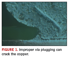
Imagine a BGA pad that has one side soldermask-defined, as a result of misalignment, and the other metal-defined. The solder collapse will not be uniform. During reflow, the soldermask will expand on the one side, creating pressure on the sphere, which acts as a lever. This can promote joint cracking.
Inadequate copper preparation will result in nonuniform coverage of an OSP coating. This is true for all surface finishes, though shortcuts often are taken at the cleaner and microetch steps of a process. If the copper surface has contaminants, the finish will not properly bond to the copper. This can manifest itself as nonuniform coverage, poor surface coating adhesion, insufficient thickness, solder joint voiding, and even premature tarnishing.
Also true for any surface finish is the importance of coating thickness. Believe it or not, thickness specifications were put on the technical datasheets for a reason. The specified thickness is critical to the coating’s performance. Everyone has experienced an insufficiently plated tin deposit. After one reflow, all the pure tin had been quenched by intermetallic that laughed at you on the second assembly pass.
Focusing on process flow and routine analysis can eliminate many future quality issues. Did you know sending a board twice through Pb-free HASL can embrittle the soldermask to the point where the resultant product will have much worse creep corrosion than any thin immersion silver deposit? Did you know the first instance of soldermask interface attack on an immersion silver board was found as a result of a customer continuously dragging microetch into the following rinse, which did not have a sufficiently strong turnover? Basically, the PCBs were being double-etched, and then put directly into the pre-dip bath.
On a positive note, running the right process controls can make a better product. Choosing the proper equipment for immersion tin can minimize solution air exposure and extend bath life. Premature tin oxidation and thiourea decomposition can be greatly reduced. Using the right pre-clean, including a well-maintained microetch, can enhance the OSP and immersion silver coating quality, which in both cases enhances solderability.
Maybe you do realize all this. But did you realize how much research at a chemical supplier goes into widening an operating window to accommodate the “what ifs” in fabrication? It is amazing what is asked of the surface finish on a day-to-day basis.
I don’t want this to be a finger-pointing exercise. I want to provoke thoughts on how to make process control second nature. I want to expose the synergy of the fabrication, assembly and end use performance. Every detail affects the next step and ultimately the final product.
When I started on this journey, I learned quickly that there was an application for each surface finish. They all have strengths and weaknesses. If processes are run according to specifications provided, and the same can be said for the processes around them, the resultant product will be superior. There are many instances where a coating outperforms the expectations of the chemical supplier, fabricator assembler and end-user. Imagine a surface finish produced as a result of everything run under optimal conditions: superhero status.
Lenora Toscano is final finish product manager at MacDermid (macdermid.com); ltoscano@macdermid.com.

Radiated emissions must be designed out at the beginning.
If your last product passed FCC certification and shipped on time, pat yourself, your EMC engineer and your design team on the back. You accomplished something that is really hard and doesn’t usually happen by accident.
Of the various EMC certification tests, FCC Part 15 Class B, which applies to consumer products, is one of the most stringent. In the roughly 100 MHz range, the maximum allowed radiated emissions from a fully functioning product, when measured 3 meters away, within a 120 kHz bandwidth, must be less than about 100 µV/m.
To put this in perspective, what do you think is the maximum power a radio station could transmit, into a 120 kHz bandwidth, and still pass this FCC test? Is it 1 W? One mWatt? One microwatt?
The answer is shocking. A radio station would have to radiate less than 10 nW of power into a 120 kHz bandwidth in order to pass certification. That is hard.
The most common reason for products to fail this test is due to radiation from common currents on external cables. For a cable 1 meter long, it only takes a common current of 3 µA to radiate enough to fail a certification test.
When you consider that a 1 V signal, driving into a 50 Ω line, is a current of 20 mA, you see that the common currents must be less than 0.01% of the signal currents. This is why passing EMC tests is difficult.
I have yet to encounter a single large system company that does not have a horror story to tell about a product that worked great, passed all the functional tests, but either was never able to pass FCC certification or took so long to fix an EMI problem that its release was late and it missed the market window.
One doesn’t pass an FCC test by accident. It is by designing radiated emissions out of the product right from the beginning, and, in instances where they can’t be designed out, adding filters and shielding to minimize their impact on the certification test.
Don’t expect to learn how to design a product to pass an EMC certification test by following a list of 10 habits. But, if you want a list of topics to use as a guide to begin the discussions in your design team, here are my recommendations for the Top 10 Habits to increase the probability of passing an EMC certification test:
- Ground bounce drives common currents on external cables. Minimize ground bounce in all the components of the system.
- Use shielded cables. The cable shield should be an extension of the enclosure, not connected to the ground planes of circuit boards. Cable connectors should make a 360° connection between the shield and enclosure.
- All control wires and cables that leave the board, even if just routed inside the enclosure, should be routed with an adjacent return conductor. Use as long a rise time as can be afforded for all signals that leave the board. Increase rise times with filters.
- Use ferrites around the outside of external cables to suppress common currents.
- Minimize mode conversion in all differential channels that leave the enclosure.
- Add common signal chokes to all differential signals that leave the enclosure.
- The largest source of noise, above 50 MHz, that gets into the power and ground network is from signals passing through the power and ground cavity. Manage this noise with return vias, differential signaling and decoupling capacitors adjacent to signal vias. Smart stack design up can enable the use of return vias.
- Design the stackup so that power and ground planes are on adjacent layers, with as thin a dielectric as possible, and preferably close to the board surfaces.
- Plan on using a spread spectrum clock generator to smear the first harmonic of all signals into a wider bandwidth. The FCC receiver has a 120 kHz bandwidth. Spreading the spectrum of each harmonic over 1.2 MHz reduces the average power detected in the FCC test by 10 dB.
- Enclosure design is not about designing enclosures; it is about designing apertures and seams.
If you weren’t aware of these guidelines when you designed and built your last product, you may have been lucky and dodged a bullet. Don’t rely on luck for your next design. Bring up these topics in the next design review. Have SI engineers and EMC engineers explain what they mean. If still not clear on the concepts, or how to implement them, read a book, find an expert or take a class.
Dr. Eric Bogatin is a signal integrity evangelist with Bogatin Enterprises, and has authored six books on signal integrity and interconnect design, including Signal and Power Integrity – Simplified, published in 2009; eric@bethesignal.com.

Despite the downturn, several EMS companies found ways to improve workers’ lives both in and outside the plant.
With organizations tightly watching costs and a steady stream of headlines on (high) unemployment rates, it would be easy to assume that companies are no longer willing to invest in their employees. When I surveyed several EMS providers in February, however, I found nothing could be further from the truth. While programs varied, the common link was that all these companies saw investments in improving employee quality of life and skills as a practice that contributed to the bottom line. I selected some program highlights from operations in the US, Mexico, Singapore and Poland to provide a broader look at variations between countries and cultures.
MEC. According to Rick McClain, general manager of MEC NW’s Canby, OR facility, MEC chose to invest in employee development during the downturn by keeping a trainer on staff and enhancing internal capabilities. Training focused on a mix of IPC-A-610 certification training and in-house systems training. One result is that the company recently added IPC-A-610 Class III assembly capability.
There also is a strong focus on continuous improvement (CI). Employees are encouraged to submit CI suggestions that improve one or more of eight identified areas of waste: waiting, rework, overprocessing, transportation, inventory, overproduction, unused employee creativity or motion. At a facility level, MEC has a game similar to the TV show Amazing Race. In this “race,” employees pick a spot on a world map and then earn “miles” based on tracked company improvements. Metrics tracked are revenue, on-time shipments, warranty returns, employee improvements implemented, parts per million (PPM) defect rates and employee fitness (i.e., miles walked, swam or biked). A conversion chart is used to assign miles to each category. If the target mileage is hit, there is a luncheon and prizes that reflect the country originally targeted on the map.
As the metrics example indicates, there is also a wellness program. The company hosts an annual Wellness Fair featuring 10 to 20 vendors and benefits specialists who offer advice on fitness options. Biometric screenings for employees are free, and results are translated to recommendations for a healthier lifestyle. Fitness activities such as walking are encouraged and there is monthly recognition for employees living healthy lifestyles. Fitness club discounts have been negotiated as well.
EPIC Technologies. EPIC Technologies maintains a strong focus on worker training and quality of life in its US and Mexico operations. Here, we focus strictly on its programs in Juarez, Mexico. Mexican law mandates a wide range of employee benefits related to onsite health care, bonuses, vacation and sick leave. EPIC’s programs exceed these minimums. According to Salvador Baca, EPIC’s Mexico human resources manager, good benefits are one way to reduce absenteeism, tardiness and turnover.
Although Mexican law only requires infirmaries be staffed by nurses, EPIC has an onsite doctor too. Nurses are present on all shifts and the doctor during the day. The facility provides prescription medicine and immunizations. Employee families are also treated. According to Baca, the benefit of this extra health care option is improved health for employees and less lost time, since the government’s health care system typically has long waiting times.
The company also has invested in training. A teacher conducts classes within the facility to help employees who haven’t completed high school study for their degree. After six months on the job, employees are eligible for an annual $400 scholarship for special training. In special cases, tuition reimbursement is provided for programs toward a job-related degree. Employees are also sent to schools around the country for special programs related to IPC, ISO/TS-16949, or customer-required training.
While emphasis is on CI initiatives throughout the year, EPIC drives an extra focus on quality once a year with its Race for Quality event. The race adds a competitive element to Lean projects and kaizen events for three consecutive months. Goals are set for projects for each month. If the goals are met, employees get a prize and the best-performing shift gets a double prize. Each monthly goal is more difficult, but prizes are improved as difficulty increases.
Also, focus is on social activities, as Mexico has a very family-centered culture. For example, a special Mother’s Day celebration in May includes mariachis, a special lunch and raffles for all employees who are mothers. Families are invited to an annual picnic in July. A Christmas party for employees in December includes a special dinner and gift for each employee. Sports teams also have been organized. There are internal tournaments for soccer, and the teams also play in a city league with other factories. Basketball and volleyball tournaments are held.
“These types of activities improve the company by encouraging better communications and working environment,” says Baca. “This type of teamwork and communications creates more ownership.” It is not unusual to see companies without such activities experience 25% more turnover than those that invest in expanded benefits, he adds.
Unique at EPIC is its Values Program targeted at employees’ families. Employees who sign up to participate are given monthly homework assignments to take to their children. The assignments are focused on core values such as justice and responsibility. “We want to invest in the community and send strong values messages out to families,” said Baca.
Employees who work with their children in this program are recognized by EPIC with a small gift. At the end of the year, EPIC has a party with the families that participate.
CEI Contract Manufacturing. During the downturn, when asked if layoffs would help create better shareholder value, CEI contract manufacturing managing director Ka Huat Tan replied, “Do you want to create shareholder value for the next three months or the next 10 years?” Not only did the Singapore-based EMS company have no layoffs, it continued to pay small bonuses.
“When times are hard, people become uncertain and edgy,” Tan said. “It is important to make sure people feel valued. CEI is very sensitive to that. We had our HR department informally communicate that there would be no layoffs. During the worst of the downturn, we kept our staff busy with additional training, funded in part through Singapore Economic Development Board incentives. We also bought a new factory with gross space of 40,000 sq. ft. and continued to invest in new technology, which signaled employees we were committed to long-term growth.”
That decision also had positive impact on the bottom line. In 2009, the company received nearly S$600,000 in job credit incentives because it maintained its employment levels.
Tan believes people are a company’s most important asset, but cautions that simply stating that is meaningless if not backed by actions. For example, Tan asked his managers to watch for employees who might be experiencing financial difficulties. While the company didn’t provide cash in those cases, it did provide informal assistance, including suggestions on contacts or resources that could help. “The goal wasn’t to give employees in financial trouble a handout, but instead create a supportive environment that made it easier for them to fix the issues themselves,” said Tan.
CEI has a Work Life Balance committee that consists of a safety committee, a sports committee, a special interest group committee and an HR committee.
The company’s Wellness Program is quite comprehensive. HR organizes a 1.5 to 2 hr. quarterly seminar that focuses on health-related topics such as stress management.
Sports teams have been organized for bowling, table tennis and badminton. The company also holds a Sports Day at a local stadium and gets almost 100% employee attendance at the event. There is a recreation room in the facility used for table tennis and yoga classes. A gym with a treadmill, cross trainers and a fitness instructor were recently added.
CEI funded 80% of a 2009 medical checkup to encourage all staff to have diagnostic testing. This testing program provides them with a measure of the general health of the company’s employees that can be compared to Singapore averages. “The statistics show there is room for improvement. Part of showing you care about employees is identifying areas for personal improvement and encouraging them to improve. By studying overall health trends and tracking sick leave, we can tell who abuses sick leave and who truly has health issues that need to be accommodated,” said Tan.
At the last dinner dance, the organizing committee invited staff members who have been exercising to talk about what they’ve learned in the process. Participation in extracurricular wellness activities is part of the equation in determining the size of an employee’s bonus. But CEI’s program also has punitive measures. A pattern of sick leave abuse can impact annual bonuses.
Tan sums it up simply: “We try to encourage the best in our employees, but also have checks and balances to address issues such as sick leave abuse.”
Kimball Electronics Group. Kimball has strong programs for sharing corporate values and incenting individual employee development. According to Julie Dutchess, Kimball Electronics Group’s global HR director, the company has been administering Vision and Guiding Principles Surveys in its Poznan, Poland, facility since 2004. In 2007, the Poland group included an additional step in the survey process to provide group and production unit leaders with 360° feedback on softer management skills. Employees’ comments for improvement in previous guiding principle surveys were used as criteria in the feedback process.
“Polish culture always placed high value on work ethic and accomplishing goals, and when they added focus on the softer interpersonal relationship management skills, they could see the positive impact,” Dutchess said. “The survey allows us to measure how supervisors and managers are improving in terms of the way they manage. Tracking rating trends the same way we track metrics for on-time delivery or quality has helped the staff to realize the importance of this area of management skills, and we have seen visible improvement over time.”
Another area of improvement has been in worker skills. Originally, employees’ jobs were focused fairly narrowly. As the company’s customer base has grown in size and diversity, so has the need for greater flexibility on the floor. Keeping headcount the same meant training operators for several job stations.
“Originally people didn’t like this. They were used to doing the same job. We told them that if they were willing to develop themselves and gain new knowledge through training, their promotion ability and earning potential would grow. Some embrace this; others do not,” said Magdalena Okon, the Poland facility’s HR manager.
The new program created a core group of employees called multi-operators. When demand varies, Kimball can very quickly shift employees between production lines. To qualify as a multi-operator, the operator must be trained and certified for 60% of the job stations within the production area.
Multi-operators are paid more and are prioritized for promotion to higher levels, such as group leader or transfer to other departments. Okon points out that this has helped to create a clear path for career advancement on the production floor. Currently 80% of internal promotions come from the pool of production operators.
One other path for career advancement is Kimball’s Individual Development Program. “People development is everyone’s responsibility. HR supports by providing engagement, tools and knowledge. Participants must have a vision for their career. Kimball can help, but the employee is the owner of their own development,” said Okon.
IDP has several goals:
- Development and retention of key employees.
- Assurance of successors for key management positions in the organization.
- Improved employees’ satisfaction as the result of advancement potential.
A class of candidates are selected every two years. Candidates must fill out an application that outlines long-term career aspirations and a plan to achieve them. There is a a follow-up interview with HR and their immediate supervisor. Managers in each department then nominate the employees they feel have the most development potential.
An IDP Council composed of the managers of the facility, quality, production, HR and an HR specialist reviews the nominees and chooses final participants. It is interesting to note the selection process looks at organizational resources in terms of availability of mentors and the availability of career path advancement, in addition to the relative merit of each candidate. No more than seven candidates are selected per IDP class.
Once selected, the candidate, HR and the candidate’s immediate supervisor identify the key skills that need to be developed to perform well in the final position and create a detailed plan that lists skills, development activities, responsibilities, timeline, risks, cost and status of execution. External consultants verify the level of competencies while the candidate is in development. Every six months, HR checks plan status and collects feedback from participants. The information also is discussed with the IDP Council.
“Not everyone stays,” Okon said. “In some cases, there is no path for further progression, and a candidate opts to leave the program to pursue other opportunities. We do debrief candidates who leave to determine what went well and what could be done better. It is definitely worth the risk of investing in training. In the end, even when we lose someone because the organization is not ready to utilize his or her full potential because a desired advancement opportunity isn’t available, we still have the opportunity to get some benefit from his or her talent while the candidate is growing. We would probably lose the candidate much sooner if we did no development. The program has helped fill some key slots.”
One key measure of the success of Kimball’s program is turnover. According to Okon, while voluntary turnover in the Poznan region averages 8% per year, Kimball’s Poland facility’s annual turnover rate is 2%.
Each of these companies has taken basic good management practices and used them creatively to increase motivation and productivity, reduce turnover and improve employee quality of life. Given that employees are often the key differentiators between one EMS provider and another, it appears money well spent.
Susan Mucha is president of Powell-Mucha Consulting Inc. (smucha@powell-muchaconsulting.com), a consulting firm providing strategic planning, training and market positioning support to EMS companies. Her book, Find It. Book It. Grow It. A Robust Process for Account Acquisition in Electronics Manufacturing Services, is available through barnesandnoble.com, amazon.com and the IPC and SMTA bookstores. Her column runs bimonthly.

Press Releases
- The SearchWorks Group Shares Mid-Year Read on the EMS Talent Market
- Altus Announces Return of ‘Factory of the Future’ for 2026
- Circuit Technology Center, Inc. Expands High-Volume BGA Reballing Capacity with Investment in Additional Reflow Oven
- SEMI And Global Net Corp. Release New Report On Glass Core Substrate Market And Development Trends For Semiconductors